EP0037734A2 - Halbleiterspeicherbaustein und Speicheranordnung mit solchen Bausteinen - Google Patents
Halbleiterspeicherbaustein und Speicheranordnung mit solchen Bausteinen Download PDFInfo
- Publication number
- EP0037734A2 EP0037734A2 EP81301494A EP81301494A EP0037734A2 EP 0037734 A2 EP0037734 A2 EP 0037734A2 EP 81301494 A EP81301494 A EP 81301494A EP 81301494 A EP81301494 A EP 81301494A EP 0037734 A2 EP0037734 A2 EP 0037734A2
- Authority
- EP
- European Patent Office
- Prior art keywords
- chip
- level
- lines
- voltage
- bit line
- Prior art date
- Legal status (The legal status is an assumption and is not a legal conclusion. Google has not performed a legal analysis and makes no representation as to the accuracy of the status listed.)
- Granted
Links
Images

Classifications
-
- G—PHYSICS
- G11—INFORMATION STORAGE
- G11C—STATIC STORES
- G11C11/00—Digital stores characterised by the use of particular electric or magnetic storage elements; Storage elements therefor
- G11C11/21—Digital stores characterised by the use of particular electric or magnetic storage elements; Storage elements therefor using electric elements
- G11C11/34—Digital stores characterised by the use of particular electric or magnetic storage elements; Storage elements therefor using electric elements using semiconductor devices
- G11C11/40—Digital stores characterised by the use of particular electric or magnetic storage elements; Storage elements therefor using electric elements using semiconductor devices using transistors
- G11C11/41—Digital stores characterised by the use of particular electric or magnetic storage elements; Storage elements therefor using electric elements using semiconductor devices using transistors forming static cells with positive feedback, i.e. cells not needing refreshing or charge regeneration, e.g. bistable multivibrator or Schmitt trigger
- G11C11/413—Auxiliary circuits, e.g. for addressing, decoding, driving, writing, sensing, timing or power reduction
- G11C11/414—Auxiliary circuits, e.g. for addressing, decoding, driving, writing, sensing, timing or power reduction for memory cells of the bipolar type
Definitions
- This invention relates to a semiconductor memory chip, and a memory device including such chips.
- the memory device provides a large capacity, only one chip therein is selected, so that a memory cell in a selected chip can be written or read. Other chips, and memory cells of those chips, are not selected.
- an address, for reading or writing is given to all chips, whether selected or not selected, and a word line of a non-selected chip corresponding to the selected word line of the selected chip becomes H level. At a time when this is taking place, therefore, if noise occurs on a bit line, problems such as erroneous writing can sometimes occur.
- bit line voltage in a non-selected chip has been the same as bit line voltage in a selected chip in read operation, and therefore information in a cell of a non-selected chip is also read onto a bit line of that chip, as information in a cell of a selected chip is read onto a bit line of the selected chip.
- a transistor in an OFF condition in a flip-flop type memory cell can turn ON.
- a transistor on the ON side of the memory cell may turn OFF. Namely, stored information may be destroyed.
- Power supply line noise or noise on signal lines due to, for example, a variation of input data or of address signal, can appear on bit lines.
- a semiconductor memory chip having a chip select facility , including memory cells arranged at intersection points of word lines and bit lines of the chip, wherein clamp means are provided which are operable, when the chip is non-selected, to clamp bit- line voltage to a level higher than the bit line voltage level during a read operation when the chip is selected.
- the present invention can provide a semiconductor memory device including a plurality of such chips.
- An embodiment of the present invention can offer a static semiconductor memory device in which the incidence of destruction of information stored in cells of the device is reduced.
- An embodiment of the present invention can offer a semiconductor memory device in which influence of disturbances on memory cells of a non-selected chip is reduced, and which has a high memory cell holding margin.
- An embodiment of the present invention can offer a semiconductor memory device in which simple means are employed to provide a large memory cell holding margin.
- a bipolar static type semiconductor memory device comprising memory cells, each having a flip-flop circuit structure, disposed at respective intersection points of word lines and bit line, has clamp means for clamping bit line voltage, when a chip is non-selected, to a voltage higher than bit line voltage in read operation when a chip is selected.
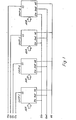
- FIG. 1 illustrates a memory device formed using four semiconductor chips.
- CHIP-1 to CHIP-4 are semiconductor memory chips and each chip has a CS terminal, the CS terminals of CHIP-1 to CHIP-4 are arranged to receive chip select signals CS 0 to CS 3 respectively, a D in terminal for receiving a data signal D in , a WE terminal for receiving a write enable signal WE, and a D out terminal for output of a data output signal D out .
- An address signal ADR is applied in common to all the chips CHIP-1 to CHIP-4. Since the address signal ADR is input in common to the chips, the address of one cell in each chip is designated, but only one of the chips is selected, by means of chip select signals CS 0 to CS 3 , and thereby input data signal D in is written into and/or output signal D out is read out of only the selected chip. Namely, a write operation for writing input data D in' and/or a read operation for output of output data D out' is inhibited at a non-selected chip by the relevant chip select signal.
- An embodiment of the present invention relates to a semiconductor memory chip suitable for use in a structure wherein a plurality of semiconductor memory chips are combined, for example as shown in Figure 1.
- a semiconductor memory chip embodying this invention can offer improved circuits within the chip and can assure high memory cell holding margin.
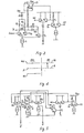
- Figure 2 is a schematic diagram of a memory cell area of a static semiconductor memory embodying the present invention
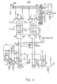
- Figure 3 is a schematic diagram of a READ/WRITE control circuit of the memory
- Figure 4 is a voltage level chart for assistance in explanation of the memory of Figures 2 and 3.
- a clamp circuit CL is provided as shown in Figure 3, the structure of the circuitry shown in Figure 2 and that of circuits other than CL in Figure 3 is generally conventional.
- a read.level e.g. base voltage of a read transistor connected to a bit line, except when data is being written in through the read transistor in a memory chip
- bit line voltage in non-selected chips has been the same as bit line voltage in a selected chip, during a read operation.
- the voltage chart of Figure 4 is for assistance in explaining this relationship.
- SEL indicates a part of the chart relating to a case in which a chip is selected
- NS indicates a part of the chart relating to a case in which a chip is not selected.
- WE is a H(high) write level corresponding, for example, to data "1”
- WL is a L(low) write level, in this example, corresponding to data "0”.
- a read level R is set mid-way between WH and WL and,- as indicated in Figure 4, has been held at the same value for selected and not selected chip states.
- Figure 3 shows a READ/WRITE control circuit for generating levels represented in Figure 4.
- chip selection signal CS becomes H (high) level
- a transistor Q 1 is ON
- a transistor Q 2 is OFF
- a point P 1 is H level.
- the write enable signal WE is L (low) level, which low level instructs a write operation, or H (high) level, which high level instructs a read operation
- a point P 2 becomes H level, and thus a transistor Q 4 is ON
- input data signal D in is H or L
- data lines D, D are set to a constant level (R level in Figure 4) which is determined by a power supply voltage V DD , a diode d 1 , resistors R 1 , R 2 , diodes d 21 d 3 , transistor Q 4 and a constant current source J 1 .
- CS When a chip is selected, CS is L level, therefore Q 1 is OFF, Q 2 is ON, and point P 1 is L level. As a result, a transistor Q 5 , which receives the write enable signal WE, becomes effective. Moreover, when WE becomes L level, in a write operation, point P 2 becomes L level and Q 4 is OFF. Thus, a transistor Q 6 of a current switch CW 0 becomes ON or OFF, whilst another transistor Q 7 of the current switch becomes OFF or ON, and data lines D, D become H or L level in accordance with the level, H or L, of input data D. namely in dependence upon the data being "1" or "0". These H and L levels are represented by WH, WL in Figure 4.
- the D, D lines supply a reference voltage to read transistors Q 10' Q 11 inserted between bit lines (B 00' B 01 ) (B 10 ' B 11 ) as seen in- Figure 2. Namely, when a memory cell MC 00 is selected in Figure 2, read transistors Q 10' Q 11 connected to bit lines B 00 , B O1 form a current switch in combination with transistors Q 12 , Q 13 of the memory cell MC 00 .
- a transistor state in which Q 12 is originally ON and Q 13 is originally OFF must be reversed (there is no change if the transistors are to be written in the original state) by setting the data line D to H level, and the data line D to L level.
- Q 10 becomes ON, Q 12 OFF, Q 11 OFF and Q 13 ON.
- the memory cells MC 10 , MC 01 , MC 11 are structured in the same way as the memory cell MC 00 .
- W 0 , W 1 , ... are word lines, whilst W 0-' W 1-' ... are holding lines.
- a word line is selected when an X address selection signal X 0 , X 1 , ... becomes H level.
- a bit line pair (B 00' B 01 ), (B 14' B 11 ) ... is selected when a Y address selection signal Y 0 , Y 1' ... becomes H level.
- Embodiment of the present invention are intended to offer an improvement in relation to this disadvantage.
- it is intended to reduce the effects of disturbance on a memory cell and to ensure a large memory cell holding margin by making the read (R) level higher in the non-selected condition.
- R read
- a bit line clamp level higher than the read level R in a selected condition, as indicated by RL in Figure 4, is used.
- the degree to which read level is increased in the non-selected condition is not limited, and it can simply be provided, for example as shown in Figure 3, by the provision of a clamp circuit CL consisting of a transistor Q 8 and connected as shown.
- the transistor Q 8 clamps the data lines D, D to V DD - V BE level because CS is H level, and P 1 is H level (here V BE is the base-emitter voltage of transistor Q 8 ).
- Figure 5 illustrates READ/WRITE control circuitry of another embodiment of the present invention.
- current switches CW 1 , CW 2 are added to a conventional circuit structure - other parts of the circuitry correspond almost exactly to Figure 3 (accurately, the diode d 1 used in Figure 3 is omitted).
- Figure 6 illustrates a further embodiment of the present invention.
- MC 11 to MC 22 are memory cells which are selected by word lines W 1 , W 2 and bit line pairs B 00 and B 01 , B 10' B 11'
- word lines W 1 , W 2 and bit line pairs B 00 and B 01 , B 10' B 11' Of course many word lines, bit lines and memory cells are provided. However, in Figure 6, only four memory cells are indicated. In the case of the memory cells in Figure 6, a word line is selected by addresses X 0 , X 1 , while bit lines are selected by Y addresses A 0 , A 1 and A 2 . A current switch CW 3 generates A 0 and inverted A 0 . Similar circuits are also provided (although they are not illustrated) for address bits A 1 , A 2 to generate A 1 , A 1 and A 2 , A 2 and these are connected to wiring AL.
- Transistors Q 31' Q 32 and Q 33' Q 34 are inserted in the bit lines and the bases of these transistors are connected to the wiring AL and the relevant bit line becomes effective only when these transistors are all OFF.
- Read transistors Q 35' Q 36' Q 37 are also connected to the bit lines and their bases are arranged to receive a read level (R) in common and thereby these transistors can read stored data by forming a current switch in combination with the ON transistor of a memory cell connected to a selected word line (for example, when MC 11 is selected and its left side transistor is ON, Q 35 is OFF, while Q 36 is ON, thus a current does not flow into one line of a sense amplifier but does flow into the other line and thereby the sense amplifier SA can detect the stored content of MC 11 ).
- the read level in non-selected condition can be increased by clamping all of the decoders lines AL to H level under a condition in which a chip is not selected. Namely, when a chip is not selected, the chip select signal CS is H, and therefore a point P 3 becomes H level.
- a base voltage for read transistor Q 35 is generated by a circuit as indicated in the lower left side of Figure 6.
- CS is L level
- P 3 is L level when a chip is selected and a read operation is to be carried out. Therefore, a transistor Q 41 is OFF and a write enable signal WE is H level and as a result transistors Q42, Q 43 are ON, a transistor Q 44 is OFF and a voltage at emitter point P 3 ' of a transistor Q 45 becomes H level. Voltage of point P 3 ' at this time becomes a read level R.
- J4 is a current source
- R 5 to R 8 are resistors
- W represents hold lines.
- the embodiments of Figures 2, 3 and 5 operate to clamp the base voltage of a read transistor to a high level in a non-selected chip in read operation
- the embodiment of Figure 6 operates to clamp the base voltage of a bit line selection transistor in a non-selected chip in read operation.
- An embodiment of this invention relates to a bipolar static type semiconductor memory device in which the influence of disturbances on the memory cells of non-selected chips is reduced and a large memory cell holding margin is obtained.
- a semiconductor memory device embodying the present invention comprises memory cells, each of a flip-flop circuit structure, at respective intersection points of the word lines and bit lines.
- the memory holding margin of the memory cells is increased by providing a clamp means which clamps bit line voltage in a non-selected condition to a voltage higher than the bit line voltage in a read operation when a chip is selected.
- An embodiment of the present invention provides a bipolar static type semiconductor memory chip, having a chip select facility, including memory cells, each having a flip-flop circuit structure, arranged at intersection points of word lines and bit lines of the chip, wherein clamp means are provided which are operable, when the chip is non-selected, to clamp bit line voltage to a level higher than the bit line voltage level during a read operation when the chip is selected.
- a semiconductor memory device embodying the present invention may comprise a plurality of chips as specified immediately above.
Landscapes
- Engineering & Computer Science (AREA)
- Microelectronics & Electronic Packaging (AREA)
- Computer Hardware Design (AREA)
- Static Random-Access Memory (AREA)
Applications Claiming Priority (2)
| Application Number | Priority Date | Filing Date | Title |
|---|---|---|---|
| JP55045826A JPS6034189B2 (ja) | 1980-04-08 | 1980-04-08 | 半導体記憶装置 |
| JP45826/80 | 1980-04-08 |
Publications (3)
| Publication Number | Publication Date |
|---|---|
| EP0037734A2 true EP0037734A2 (de) | 1981-10-14 |
| EP0037734A3 EP0037734A3 (en) | 1983-06-29 |
| EP0037734B1 EP0037734B1 (de) | 1986-12-30 |
Family
ID=12730039
Family Applications (1)
| Application Number | Title | Priority Date | Filing Date |
|---|---|---|---|
| EP81301494A Expired EP0037734B1 (de) | 1980-04-08 | 1981-04-07 | Halbleiterspeicherbaustein und Speicheranordnung mit solchen Bausteinen |
Country Status (5)
| Country | Link |
|---|---|
| US (1) | US4432076A (de) |
| EP (1) | EP0037734B1 (de) |
| JP (1) | JPS6034189B2 (de) |
| DE (1) | DE3175776D1 (de) |
| IE (1) | IE52476B1 (de) |
Families Citing this family (3)
| Publication number | Priority date | Publication date | Assignee | Title |
|---|---|---|---|---|
| US4658160A (en) * | 1985-10-01 | 1987-04-14 | Intel Corporation | Common gate MOS differential sense amplifier |
| US6016390A (en) * | 1998-01-29 | 2000-01-18 | Artisan Components, Inc. | Method and apparatus for eliminating bitline voltage offsets in memory devices |
| JP4579965B2 (ja) * | 2007-12-19 | 2010-11-10 | パナソニック株式会社 | 半導体記憶装置 |
Family Cites Families (4)
| Publication number | Priority date | Publication date | Assignee | Title |
|---|---|---|---|---|
| US3729721A (en) * | 1970-09-23 | 1973-04-24 | Siemens Ag | Circuit arrangement for reading and writing in a bipolar semiconductor memory |
| US3781828A (en) * | 1972-05-04 | 1973-12-25 | Ibm | Three-dimensionally addressed memory |
| US4099070A (en) * | 1976-11-26 | 1978-07-04 | Motorola, Inc. | Sense-write circuit for random access memory |
| JPS5847792B2 (ja) * | 1979-07-26 | 1983-10-25 | 富士通株式会社 | ビット線制御回路 |
-
1980
- 1980-04-08 JP JP55045826A patent/JPS6034189B2/ja not_active Expired
-
1981
- 1981-03-31 US US06/249,684 patent/US4432076A/en not_active Expired - Fee Related
- 1981-04-07 DE DE8181301494T patent/DE3175776D1/de not_active Expired
- 1981-04-07 IE IE784/81A patent/IE52476B1/en not_active IP Right Cessation
- 1981-04-07 EP EP81301494A patent/EP0037734B1/de not_active Expired
Also Published As
| Publication number | Publication date |
|---|---|
| IE52476B1 (en) | 1987-11-11 |
| JPS6034189B2 (ja) | 1985-08-07 |
| EP0037734A3 (en) | 1983-06-29 |
| DE3175776D1 (en) | 1987-02-05 |
| IE810784L (en) | 1981-10-08 |
| US4432076A (en) | 1984-02-14 |
| EP0037734B1 (de) | 1986-12-30 |
| JPS56143588A (en) | 1981-11-09 |
Similar Documents
| Publication | Publication Date | Title |
|---|---|---|
| US4078261A (en) | Sense/write circuits for bipolar random access memory | |
| EP0178950A2 (de) | Bipolares Transistor-Direktzugriffsspeichergerät mit einer Redundanzkonfiguration | |
| EP0019988B1 (de) | Wortleitung-Ansteueranordnung für einen Schreib-Lesebipolarspeicher | |
| US4984207A (en) | Semiconductor memory device | |
| US5016214A (en) | Memory cell with separate read and write paths and clamping transistors | |
| EP0055551A2 (de) | Ausgangspufferschaltung | |
| US4198698A (en) | Chip select power-down control circuitry | |
| US4460984A (en) | Memory array with switchable upper and lower word lines | |
| US4651302A (en) | Read only memory including an isolation network connected between the array of memory cells and the output sense amplifier whereby reading speed is enhanced | |
| EP0019381A1 (de) | Halbleiterspeicher mit Adressensignalpegeleinstellung | |
| EP0018192A1 (de) | Programmierbare, mit Adressierschaltungen versehene, bipolare Festwertspeichervorrichtung | |
| EP0037734A2 (de) | Halbleiterspeicherbaustein und Speicheranordnung mit solchen Bausteinen | |
| US4196363A (en) | Open collector bit driver/sense amplifier | |
| US3820086A (en) | Read only memory(rom)superimposed on read/write memory(ram) | |
| EP0418794B1 (de) | Halbleiterspeicheranordnung | |
| EP0130414A2 (de) | Verzeichnisspeicher | |
| US4456979A (en) | Static semiconductor memory device | |
| US4730275A (en) | Circuit for reducing the row select voltage swing in a memory array | |
| EP0023408B1 (de) | Halbleiterspeicher mit integrierten injektionslogischen Speicherzellen | |
| US4635231A (en) | Semiconductor memory with constant readout capability | |
| US4899311A (en) | Clamping sense amplifier for bipolar ram | |
| GB2135550A (en) | Semiconductor memory device | |
| JPH0318273B2 (de) | ||
| KR830001005B1 (ko) | 데코더 회로 | |
| IE54366B1 (en) | Method for writing in static semiconductor memory |
Legal Events
| Date | Code | Title | Description |
|---|---|---|---|
| PUAI | Public reference made under article 153(3) epc to a published international application that has entered the european phase |
Free format text: ORIGINAL CODE: 0009012 |
|
| AK | Designated contracting states |
Designated state(s): DE FR GB NL |
|
| RBV | Designated contracting states (corrected) |
Designated state(s): DE FR GB NL |
|
| PUAL | Search report despatched |
Free format text: ORIGINAL CODE: 0009013 |
|
| AK | Designated contracting states |
Designated state(s): DE FR GB NL |
|
| 17P | Request for examination filed |
Effective date: 19831216 |
|
| GRAA | (expected) grant |
Free format text: ORIGINAL CODE: 0009210 |
|
| AK | Designated contracting states |
Kind code of ref document: B1 Designated state(s): DE FR GB |
|
| ET | Fr: translation filed | ||
| REF | Corresponds to: |
Ref document number: 3175776 Country of ref document: DE Date of ref document: 19870205 |
|
| PLBE | No opposition filed within time limit |
Free format text: ORIGINAL CODE: 0009261 |
|
| STAA | Information on the status of an ep patent application or granted ep patent |
Free format text: STATUS: NO OPPOSITION FILED WITHIN TIME LIMIT |
|
| 26N | No opposition filed | ||
| PGFP | Annual fee paid to national office [announced via postgrant information from national office to epo] |
Ref country code: GB Payment date: 19930202 Year of fee payment: 13 |
|
| PGFP | Annual fee paid to national office [announced via postgrant information from national office to epo] |
Ref country code: FR Payment date: 19930429 Year of fee payment: 13 |
|
| PGFP | Annual fee paid to national office [announced via postgrant information from national office to epo] |
Ref country code: DE Payment date: 19930622 Year of fee payment: 13 |
|
| PG25 | Lapsed in a contracting state [announced via postgrant information from national office to epo] |
Ref country code: GB Effective date: 19940407 |
|
| GBPC | Gb: european patent ceased through non-payment of renewal fee |
Effective date: 19940407 |
|
| PG25 | Lapsed in a contracting state [announced via postgrant information from national office to epo] |
Ref country code: FR Effective date: 19941229 |
|
| PG25 | Lapsed in a contracting state [announced via postgrant information from national office to epo] |
Ref country code: DE Effective date: 19950103 |
|
| REG | Reference to a national code |
Ref country code: FR Ref legal event code: ST |