EP0037850A2 - Auf Lesespeicher gestützte, parallele digitale arithmetische Anordnung - Google Patents
Auf Lesespeicher gestützte, parallele digitale arithmetische Anordnung Download PDFInfo
- Publication number
- EP0037850A2 EP0037850A2 EP80105733A EP80105733A EP0037850A2 EP 0037850 A2 EP0037850 A2 EP 0037850A2 EP 80105733 A EP80105733 A EP 80105733A EP 80105733 A EP80105733 A EP 80105733A EP 0037850 A2 EP0037850 A2 EP 0037850A2
- Authority
- EP
- European Patent Office
- Prior art keywords
- input
- rom
- digital
- output
- parallel
- Prior art date
- Legal status (The legal status is an assumption and is not a legal conclusion. Google has not performed a legal analysis and makes no representation as to the accuracy of the status listed.)
- Granted
Links
Images



Classifications
-
- G—PHYSICS
- G06—COMPUTING OR CALCULATING; COUNTING
- G06F—ELECTRIC DIGITAL DATA PROCESSING
- G06F7/00—Methods or arrangements for processing data by operating upon the order or content of the data handled
- G06F7/38—Methods or arrangements for performing computations using exclusively denominational number representation, e.g. using binary, ternary, decimal representation
- G06F7/48—Methods or arrangements for performing computations using exclusively denominational number representation, e.g. using binary, ternary, decimal representation using non-contact-making devices, e.g. tube, solid state device; using unspecified devices
- G06F7/52—Multiplying; Dividing
- G06F7/523—Multiplying only
- G06F7/5235—Multiplying only using indirect methods, e.g. quarter square method, via logarithmic domain
-
- G—PHYSICS
- G06—COMPUTING OR CALCULATING; COUNTING
- G06F—ELECTRIC DIGITAL DATA PROCESSING
- G06F1/00—Details not covered by groups G06F3/00 - G06F13/00 and G06F21/00
- G06F1/02—Digital function generators
- G06F1/03—Digital function generators working, at least partly, by table look-up
- G06F1/035—Reduction of table size
-
- G—PHYSICS
- G06—COMPUTING OR CALCULATING; COUNTING
- G06F—ELECTRIC DIGITAL DATA PROCESSING
- G06F1/00—Details not covered by groups G06F3/00 - G06F13/00 and G06F21/00
- G06F1/02—Digital function generators
- G06F1/03—Digital function generators working, at least partly, by table look-up
- G06F1/035—Reduction of table size
- G06F1/0353—Reduction of table size by using symmetrical properties of the function, e.g. using most significant bits for quadrant control
-
- G—PHYSICS
- G06—COMPUTING OR CALCULATING; COUNTING
- G06F—ELECTRIC DIGITAL DATA PROCESSING
- G06F1/00—Details not covered by groups G06F3/00 - G06F13/00 and G06F21/00
- G06F1/02—Digital function generators
- G06F1/03—Digital function generators working, at least partly, by table look-up
- G06F1/035—Reduction of table size
- G06F1/0356—Reduction of table size by using two or more smaller tables, e.g. addressed by parts of the argument
-
- G—PHYSICS
- G06—COMPUTING OR CALCULATING; COUNTING
- G06F—ELECTRIC DIGITAL DATA PROCESSING
- G06F7/00—Methods or arrangements for processing data by operating upon the order or content of the data handled
- G06F7/38—Methods or arrangements for performing computations using exclusively denominational number representation, e.g. using binary, ternary, decimal representation
- G06F7/48—Methods or arrangements for performing computations using exclusively denominational number representation, e.g. using binary, ternary, decimal representation using non-contact-making devices, e.g. tube, solid state device; using unspecified devices
- G06F7/544—Methods or arrangements for performing computations using exclusively denominational number representation, e.g. using binary, ternary, decimal representation using non-contact-making devices, e.g. tube, solid state device; using unspecified devices for evaluating functions by calculation
- G06F7/552—Powers or roots, e.g. Pythagorean sums
-
- G—PHYSICS
- G06—COMPUTING OR CALCULATING; COUNTING
- G06F—ELECTRIC DIGITAL DATA PROCESSING
- G06F2101/00—Indexing scheme relating to the type of digital function generated
- G06F2101/08—Powers or roots
-
- G—PHYSICS
- G06—COMPUTING OR CALCULATING; COUNTING
- G06F—ELECTRIC DIGITAL DATA PROCESSING
- G06F2207/00—Indexing scheme relating to methods or arrangements for processing data by operating upon the order or content of the data handled
- G06F2207/552—Indexing scheme relating to groups G06F7/552 - G06F7/5525
- G06F2207/5523—Calculates a power, e.g. the square, of a number or a function, e.g. polynomials
Definitions
- a fully-parallel digital arithmetic device for obtaining the square, C 2 , of a value, C, via parts of the value C and involving a reduction in memory requirements.
- Three square function ROM's are employed, one responsive to the most significant-bits half of a parallel input, the second ROM responsive to the least-significant bits half of the parallel input, and the third one responsive to the sum of said most significant bits and least-significant bits.
- the outputs of the square function ROM's are then combined and scaled to effect a square by parts of the applied input value, C.
- a pair of such arithmetic devices may be advantageously combined to economically effect the product AB of two values, A and B, in the manner of a quarter square multiplier.
- the field of the invention relates to digital arithmetic means, and more particularly to digital arithmetic means employing parallel digital coding for obtaining the square of a number or value.
- the zero detector commands a zero product output without referencing or addressing the ROM, while the comparator routes the larger of A and B to a major side of an abbreviated memory matrix, the redundant portion of the matrix being omitted from the memory. While the economy achieved is better than 50%, such result is not significant in terms of the mechanization demands made by current highly sophisticated, high-density digital-data processors.
- a fully parallel quarter-square multiplier employing two sets of square-function ROM's, each responsive to a respective one of the two values A and B.
- Each such set of ROM's is arranged to cooperate as a fully parallel digital-arithmetic device for obtaining the square of a value via parts thereof.
- a first one of the square function ROM's is responsive to the most-significant-bits half of a parallel input
- the second ROM is responsive to the least-significant-bits half of the parallel input
- the third ROM responsive to the sum of the two input halves.
- a square by parts is effected by combining and scaling the outputs of the three ROM's, by which substantial economies in required memory, processing time, power and energy are obtained.
- a still further object is to provide a highly efficient digital quarter-square multiplier based on a square-by-parts technique.
- Yet another object is to provide a highly useful digital arithmetic device for the improvement of complex multipliers, including applications to FFT-butterfly arithmetic.
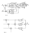
- Fig. 1 there is illustrated in block diagram form one aspect of the invention, namely a fully parallel digital arithmetic device for obtaining the square, C 2 , of a value, C.
- the device of Fig. 1 has 16 parallel inputs (corresponding to 2 16 or 65,536 unsigned addresses), although the concept of the invention is not so limited and any even number of unsigned addresses may be used.
- the square of a number is positive, whereby a sign designator is not to be contemplated, yet a modification is required in the case of a signed number which is expressed as 2's complement, as discussed later herein.
- ROM's read-only memories 11, 12 and 13.
- a read address or input of first ROM 11 and an input of a first digital summing means 14 are commonly coupled to a most-significant bits (MSB) half 19 of the parallel input 21 of the digital arithmetic device of Fig. 1.
- a read address of second ROM 12 and a second input of first digital summer 14 are commonly coupled to the least significant bits (LSB) half 20 of input 21.
- a read address of third RCM 13 is responsively coupled to the output of element 14, whereby ROM 13 is responsive to the sum of the MSB input 19 and LSB input 20.
- second and third digital combining means 15 and 16 each having a first, second and third input and an output.
- Each of the inputs of element 15 is responsively coupled to a mutually exclusive one of the read-outs of RCM's 11, 12 and 13, for providing an output indicative of the difference between the read-out of ROM 13 and the sum of the read-outs of ROM's 11 and 12.
- Each of the three inputs of third digital combining means 16 is input coupled to a mutually exclusive one of the read-outs of ROM's 11, 12 and 13 to provide an output 23 indicative of the sum of the inputs thereto.
- first gain scaling means 17 provides a gain-scaling or factor of 2 N for the input 25 to element 16 from ROM 11
- second gain-scaling means 18 provides a gain-scaling or factor of 2 N/2 for the input 24 to element 16 from element 15, where N corresponds to the number of parallel inputs.
- N 16.
- such relative gain-scaling among the three inputs to element 16 may be obtained by commonly reducing or attenuating the relative gains of all three inputs by the factor 2 -N .
- the relative gain for line 25 becomes 2 N-N or 2 0 or unity
- the relative gain on line 24 becomes 2 N/2-N or 2 -N/2
- the gain-scaling to be inserted in line 22 would be 2 -N .
- a value C applied to the 16-bit parallel digital input 21 is treated as a first partial (MSB) input, C M (corresponding to the most significant bits half of the C input) and second partial (LSB) input, C (corresponding to the remaining or least significant bits half of the value C).
- MSB first partial
- LSB second partial
- C corresponding to the remaining or least significant bits half of the value C.
- One may therefore express C as 2 N/ 2C M + C l .
- the corresponding read-outs from ROM's 11, 12 and 13 are , and (C M + C l ) 2 , respectively.
- Equation (7) is seen to be identical to that of Equation (4), as to demonstrate that the value on output line 23 in Fig. 1 corresponds to the value C 2 in Equation (6), as to illustrate a novel square-by-parts method of mechanization.
- N 16
- two ROM's each require 2 8 -1 or 255 addresses, with 16 bits per address, a total of 255 x 16 or 4,080 bits per ROM.
- the center ROM (element 13) requires a 29-1 or 511 addresses with 18 bits per address or a total of 9,198 bits.
- the three ROM's represent a memory requirement of only 17,358 bits, one 8-bit wide two-input adder 14, one 16-bit wide three input adder/subtractor 15 and one 3-input 32-bit wide pseudo adder.
- the top and battom inputs to adder 16 are illustrated in terms of bit location, per Fig. 12. There is no addition. The bits are concatenated to form a 32-bit word, but there is no actual addition. Now, consider the center input to adder 16, per Fig. 13. Adder 16, therefore, while appearing to be a 3-input 32-bit parallel adder is in fact only an 18-bit parallel adder with additional carries to the top 6 bits.
- a basic aspect of the invention as a ROM-based fully parallel digital-arithmetic device for efficiently obtaining the square of a value by parts
- application of the device may be made to digital multiplication by the quarter-square method of Fig. 2.
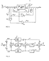
- Such quarter-square multiplier technique in Fig. 2 processes two factors A and B by means of digital combiners 31 and 32 to obtain the values [A + B] and A - B, representing the respective sum and difference thereof.
- the combination, 4AB may then be suitably scaled or attenuated (by the factor 1/4) by scaling means 35 to provide the product AB.
- the device of Fig. 1 may be employed as element 33 in Fig. 2, as shown more particularly in Fig. 3.
- An economy in organization of the device of Fig. 3 may be effected by oombining the outputs of the ROM's of the lower one of multipliers 33 in Fig. 3 with those of the corresponding ones of the upper multiplier, as shown in Fig. 4.
- Such combining of like ROM's is effected in Fig. 4 by means of adders 36, 136 and 236, as to allow the common use of a single set of elements 15 and 16, and gain channels 117, 118 and 122.
- the factor 1/4 or 2 -2 may be included in the channel scaling provided by the 16-bit elements 117, 118 and 122 in Fig. 4.
- the factor 2 N becomes 2 N-2
- 2 N/2 becomes 2 N-2
- unity or 2 0 becomes 2- 2
- the alternate scaling basis for the square function (described above in connection with the description of F ig. 1) is used, i.e., unity, 2 -N/2 and 2 -N
- the scaling factor for element 117' in Fig. 5 becomes 2 0-2 or 2 -2 , for element 118' 2 -N/2-2 and for element 122' 2 -N-2 as shown in Fig. 5.
- the sizes of the top and bottom ROM's are identical: 2 N/2 words x N bits per word, while the size of the center ROM 13 is 2 l+N/2 words x (N+2) bits per word.
- Such increase in the required size of the center ROM arises from the effect of adding or combining the two half size (2 N/2 ) words by summing means 14, as is well understood in the digital processing art.
- the increase by one in the number of output lines relative to the size of an input to element 14 may be appreciated from considering the binary addition of two like or a pair of binary two- digit numbers: the resultant sum being a three digit number.
- a standard single-size ROM be commonly used to perform the function of Fig. 9, and that such standard be based on the smaller size of elements 11 or 12 rather than that of element 13, as shown in Fig. 7.
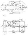
- FIG. 7 there is illustrated a block diagram of the device of Fig. 9 for a 16-bit word input and in which accommodations have been included for reducing the input size of the central ROM to N/2 bits.
- the means for such accommodation is seen to be a coincidence or AND gate 41 having a first input responsively coupled to a least significant bit line b N/2 and a second input coupled to lines N/2, a "0" (ground) input and a "1" input.
- An output of gate 41 is drivingly coupled to an input of ancillary digital combining means 42, interposed at the output of the central memory.
- the N/2 lines input to gate 41 is attenuated 2 1-N/2 by gain-scaling element 43. In this way, the arithmetic output of element 42 is always correct, despite the abbreviation of the central ROM.
- FIG. 8 there is illustrated an arrangement for a square function ROM in which there is included means for reducing the memory requirements for a square function ROM 11 by four (4) bits per word.
- a N/2 line input corresponding to a 2 N/2 word input and representing the exemplary 8-bit word input to one of the three memories in Fig. 7.
- OR gate 50 is coupled to the (N/2-2) and (N/2-1) lines of the N/2 parallel input.
- the least-significant-bit output line b N is coupled directly to the least-significant-input line a N/2 .
- the next least significant output line b N-1 is grounded.
- Output line b N-2 is coupled to the output of gate 51 which gate is in turn responsively coupled to the two least-significant input lines a N and a N/2-1 , to provide a gate output upon the coincidence of a N/2 ⁇ a N/2-1 .
- Output line b N-3 is coupled to the output of gate 52 which gate is in turn responsively coupled to input line a N/2 and the output of OR gate 50. All of the parallel inputs of the N/2-input line are fed to the ROM; the N-4 most-significant parallel outputs of the N-output line are coupled to corresponding (N-4) read-outs of the ROM.
- Equation (19) The sign bit for the squared data will always be zero (representing a positive sign), because the sign of A 2 will always be non-negative. Therefore, the (-a o ) 2 designator in Equation (19) can be discarded and the remaining sign designator term in Equation (19) corrected for any negative sign, as shown in Fig. 6. Referring to Fig. 6 there is shown a quarter square multiplier, in which acoommdation has been included for discarding the sign bit from a 2's complement signed square function.
- S the sum (A M + A l ) except for the least significant bit
- L the least significant bit.
- Equation (24) may be rewritten substituting b N/2 for b 2 N/2 :
- the right member of Equation (25) may be rearranged by factoring b N/2 from the center term and further factoring 2 -N/2 from all but the first term:
- Such abbreviation of the central ROM by means of elements 41, 42 and 43 in Fig. 7 may be alternately achieved by the rearrangement sham in Fig. 10.
- Fig. 10 there is shown an alternate arrangement of the ancillary logic associated with the central ROM of Fig. 7, whereby such ROM may be abbreviated to the same size as the other two ROM's.
- the LSB line of the output of element 14 is fed to gate 41, as before.
- gain element 43 is interposed at the output of gate 41 and is implemented as a gain doubler, and an adder 46 interposed at the N/2 lines input to gate 41 for adding the bias 2 -(N/2+1) .
- FIG. 11 A further alternate arrangement for abbreviating the requirements of the central ROM 13 of Fig. 9 is shown in Fig. 11 and is thus explained: Ancillary logic elements 41, 42, 43 and 36 (from Fig. 10) are enployed in the arrangement of Fig. 11, but with certain differences.
- the MSB line of the output from element 46 is fed directly to gate 41 (rather than the LSB line as in Fig. 10).
- the bias term injected into the 1-bit digital combiner 46 of Fig. 11 is 1 ⁇ 2 (rather than the ( value in F ig. 10 ).
- ancillary logic for abbreviating or shrinking the size of the central, or sum-of-the-parts, ROM 13 to that of the concatenating ROM's 11 and 12 (in Fig. 9).
- Such ancillary logic comprises a coincidence gate responsive to an end bit (i.e., MSB or LSB) output of element 14 and a preselectively biased balance of the output of element 14, the digital output of which gate is doubled, and the doubled output additively combined with the output of the square function means or ROM 13, the input of the ROM being responsively coupled to the output balance of element 14.
- Figs. 6, 7 and 8 including means for abbreviating or reducing the overall memory requirements therefor.
- the arrangement of Fig. 6 avoids any increase or doubling of memory requirement which would otherwise need be included due to the two's-complement sign bit.
- the arrangement of Fig. 7 reduces or abbreviates the required size of the control ROM of the three-ROM square-by-parts device to the same size as the other two ROM's, whereby a single standard-size ROM may be used.
- the arrangement of Fig. 8 effects a significant abbreviation in the required size of such standard ROM.
- the economies achieved by the ancillary logic elements employed to effect such abbreviations far exceed the nominal cost of such minor additions to the mechanization.
- the memory requirement for a square-by-parts type quarter square multiplier in which accommodations are included to employ a standard ROM is 6N(2 N/2 -1), while the memory size for such multiplier in which the standard RCM is further abbreviated as 6 (N-4) (2 N/2 -1).
Landscapes
- Engineering & Computer Science (AREA)
- Theoretical Computer Science (AREA)
- Physics & Mathematics (AREA)
- General Physics & Mathematics (AREA)
- General Engineering & Computer Science (AREA)
- Computational Mathematics (AREA)
- Mathematical Analysis (AREA)
- Pure & Applied Mathematics (AREA)
- Mathematical Optimization (AREA)
- Computing Systems (AREA)
- Complex Calculations (AREA)
Applications Claiming Priority (2)
| Application Number | Priority Date | Filing Date | Title |
|---|---|---|---|
| US130653 | 1980-03-17 | ||
| US06/130,653 US4313174A (en) | 1980-03-17 | 1980-03-17 | ROM-Based parallel digital arithmetic device |
Publications (3)
| Publication Number | Publication Date |
|---|---|
| EP0037850A2 true EP0037850A2 (de) | 1981-10-21 |
| EP0037850A3 EP0037850A3 (en) | 1984-10-24 |
| EP0037850B1 EP0037850B1 (de) | 1988-09-07 |
Family
ID=22445699
Family Applications (1)
| Application Number | Title | Priority Date | Filing Date |
|---|---|---|---|
| EP80105733A Expired EP0037850B1 (de) | 1980-03-17 | 1980-09-24 | Auf Lesespeicher gestützte, parallele digitale arithmetische Anordnung |
Country Status (5)
| Country | Link |
|---|---|
| US (1) | US4313174A (de) |
| EP (1) | EP0037850B1 (de) |
| JP (1) | JPS56143052A (de) |
| CA (1) | CA1157160A (de) |
| DE (1) | DE3072123D1 (de) |
Cited By (1)
| Publication number | Priority date | Publication date | Assignee | Title |
|---|---|---|---|---|
| EP0091214A3 (en) * | 1982-04-02 | 1985-04-17 | Ampex Corporation | Ratio comparator for digital signals |
Families Citing this family (19)
| Publication number | Priority date | Publication date | Assignee | Title |
|---|---|---|---|---|
| US4482916A (en) * | 1982-07-02 | 1984-11-13 | Rca Corporation | Automatic color control for a digital television receiver |
| US4636973A (en) * | 1982-07-21 | 1987-01-13 | Raytheon Company | Vernier addressing apparatus |
| US4588986A (en) * | 1984-09-28 | 1986-05-13 | The United States Of America As Represented By The Administrator Of The National Aeronautics And Space Administration | Method and apparatus for operating on companded PCM voice data |
| US4694416A (en) * | 1985-02-25 | 1987-09-15 | General Electric Company | VLSI programmable digital signal processor |
| US5214599A (en) * | 1986-12-19 | 1993-05-25 | Magerman David M | Advanced dimensional processing with division |
| JP2550597B2 (ja) * | 1987-08-27 | 1996-11-06 | ソニー株式会社 | 2乗器 |
| JPH0192832A (ja) * | 1987-10-02 | 1989-04-12 | Sony Corp | 逆数演算回路 |
| US5255216A (en) * | 1991-08-16 | 1993-10-19 | International Business Machines Corporation | Reduced hardware look up table multiplier |
| FR2683340A1 (fr) * | 1991-11-05 | 1993-05-07 | Sgs Thomson Microelectronics | Circuit elevateur au carre de nombres binaires. |
| KR100195178B1 (ko) * | 1992-12-31 | 1999-06-15 | 윤종용 | 제곱 계산 회로 |
| US5957999A (en) * | 1995-08-31 | 1999-09-28 | National Semiconductor Corporation | Booth multiplier with squaring operation accelerator |
| US6012078A (en) * | 1997-06-23 | 2000-01-04 | Wood; Lawson A. | Calculation unit |
| US6260056B1 (en) * | 1998-08-21 | 2001-07-10 | Ati International Srl | Circuit and method for fast squaring by breaking the square into a plurality of terms |
| US7113593B2 (en) * | 2001-03-06 | 2006-09-26 | Ericsson Inc. | Recursive cryptoaccelerator and recursive VHDL design of logic circuits |
| US7003544B1 (en) * | 2001-10-16 | 2006-02-21 | Altera Corporation | Method and apparatus for generating a squared value for a signed binary number |
| US7080114B2 (en) * | 2001-12-04 | 2006-07-18 | Florida Atlantic University | High speed scaleable multiplier |
| TWI227618B (en) * | 2003-11-28 | 2005-02-01 | Realtek Semiconductor Corp | Decoder of symmetric/asymmetric delay modulation signal and same method |
| KR101268581B1 (ko) * | 2009-11-19 | 2013-05-28 | 한국전자통신연구원 | 그룹 변조 방법 및 이를 이용한 송수신 장치 |
| US11416218B1 (en) * | 2020-07-10 | 2022-08-16 | Ali Tasdighi Far | Digital approximate squarer for machine learning |
Family Cites Families (3)
| Publication number | Priority date | Publication date | Assignee | Title |
|---|---|---|---|---|
| US3610906A (en) * | 1968-11-07 | 1971-10-05 | Burroughs Corp | Binary multiplication utilizing squaring techniques |
| US3749898A (en) * | 1971-10-26 | 1973-07-31 | Litton Systems Inc | Apparatus for multiplying binary signals based on the binomial theorem |
| US3917935A (en) * | 1974-12-23 | 1975-11-04 | United Technologies Corp | Reduction of look-up table capacity |
-
1980
- 1980-03-17 US US06/130,653 patent/US4313174A/en not_active Expired - Lifetime
- 1980-09-24 EP EP80105733A patent/EP0037850B1/de not_active Expired
- 1980-09-24 DE DE8080105733T patent/DE3072123D1/de not_active Expired
- 1980-10-31 CA CA000363763A patent/CA1157160A/en not_active Expired
-
1981
- 1981-03-16 JP JP3858381A patent/JPS56143052A/ja active Pending
Cited By (1)
| Publication number | Priority date | Publication date | Assignee | Title |
|---|---|---|---|---|
| EP0091214A3 (en) * | 1982-04-02 | 1985-04-17 | Ampex Corporation | Ratio comparator for digital signals |
Also Published As
| Publication number | Publication date |
|---|---|
| EP0037850A3 (en) | 1984-10-24 |
| US4313174A (en) | 1982-01-26 |
| CA1157160A (en) | 1983-11-15 |
| EP0037850B1 (de) | 1988-09-07 |
| DE3072123D1 (en) | 1988-10-13 |
| JPS56143052A (en) | 1981-11-07 |
Similar Documents
| Publication | Publication Date | Title |
|---|---|---|
| EP0037850A2 (de) | Auf Lesespeicher gestützte, parallele digitale arithmetische Anordnung | |
| US4616330A (en) | Pipelined multiply-accumulate unit | |
| US4727508A (en) | Circuit for adding and/or subtracting numbers in logarithmic representation | |
| US11816448B2 (en) | Compressing like-magnitude partial products in multiply accumulation | |
| US6763368B2 (en) | Method and apparatus for performing single-cycle addition or subtraction and comparison in redundant form arithmetic | |
| US4168530A (en) | Multiplication circuit using column compression | |
| US4926371A (en) | Two's complement multiplication with a sign magnitude multiplier | |
| US4555768A (en) | Digital signal processing system employing logarithms to multiply and divide | |
| US4216475A (en) | Digital beam former | |
| US4598266A (en) | Modulo adder | |
| US6018758A (en) | Squarer with diagonal row merged into folded partial product array | |
| US4064400A (en) | Device for multiplying numbers represented in a system of residual classes | |
| US5111422A (en) | Circuit arrangement for calculating product sums | |
| US4831574A (en) | Device for computing a digital transform of a signal | |
| EP0098685A2 (de) | Mehr-Bit-Kodiertechnik für verknüpfungsfähige Multiplizierer | |
| US5537345A (en) | Mathematical function processor utilizing table information | |
| US6769006B2 (en) | Method and apparatus for calculating a reciprocal | |
| EP0428942A2 (de) | Mehrere Bit umkodierender Multiplizierer | |
| US5274580A (en) | Method for calculating the inverse of a number, and computer for performing the method | |
| US3842250A (en) | Circuit for implementing rounding in add/subtract logic networks | |
| EP0499705A2 (de) | Hochleistungsdividierer mit einer Reihe von Konvergenzfaktoren | |
| Muller | " Partially rounded" small-order approximations for accurate, hardware-oriented, table-based methods | |
| EP0673564B1 (de) | Vorrichtung zur konversion einer binären gleitkommazahl in einen binären logarithmus mit der basis 2 oder dessen umkehrung | |
| US4827444A (en) | Carry skip-ahead circuit for Manchester-type adder chain | |
| US4788654A (en) | Device for real time processing of digital signals by convolution |
Legal Events
| Date | Code | Title | Description |
|---|---|---|---|
| PUAI | Public reference made under article 153(3) epc to a published international application that has entered the european phase |
Free format text: ORIGINAL CODE: 0009012 |
|
| AK | Designated contracting states |
Designated state(s): DE FR GB IT |
|
| 17P | Request for examination filed |
Effective date: 19810903 |
|
| PUAL | Search report despatched |
Free format text: ORIGINAL CODE: 0009013 |
|
| AK | Designated contracting states |
Designated state(s): DE FR GB IT |
|
| 17Q | First examination report despatched |
Effective date: 19860314 |
|
| GRAA | (expected) grant |
Free format text: ORIGINAL CODE: 0009210 |
|
| ITF | It: translation for a ep patent filed | ||
| AK | Designated contracting states |
Kind code of ref document: B1 Designated state(s): DE FR GB IT |
|
| REF | Corresponds to: |
Ref document number: 3072123 Country of ref document: DE Date of ref document: 19881013 |
|
| ET | Fr: translation filed | ||
| PLBE | No opposition filed within time limit |
Free format text: ORIGINAL CODE: 0009261 |
|
| STAA | Information on the status of an ep patent application or granted ep patent |
Free format text: STATUS: NO OPPOSITION FILED WITHIN TIME LIMIT |
|
| 26N | No opposition filed | ||
| ITTA | It: last paid annual fee | ||
| PGFP | Annual fee paid to national office [announced via postgrant information from national office to epo] |
Ref country code: FR Payment date: 19970820 Year of fee payment: 18 |
|
| PGFP | Annual fee paid to national office [announced via postgrant information from national office to epo] |
Ref country code: DE Payment date: 19970822 Year of fee payment: 18 |
|
| PGFP | Annual fee paid to national office [announced via postgrant information from national office to epo] |
Ref country code: GB Payment date: 19970826 Year of fee payment: 18 |
|
| PG25 | Lapsed in a contracting state [announced via postgrant information from national office to epo] |
Ref country code: GB Free format text: LAPSE BECAUSE OF NON-PAYMENT OF DUE FEES Effective date: 19980924 |
|
| GBPC | Gb: european patent ceased through non-payment of renewal fee |
Effective date: 19980924 |
|
| PG25 | Lapsed in a contracting state [announced via postgrant information from national office to epo] |
Ref country code: FR Free format text: LAPSE BECAUSE OF NON-PAYMENT OF DUE FEES Effective date: 19990531 |
|
| PG25 | Lapsed in a contracting state [announced via postgrant information from national office to epo] |
Ref country code: DE Free format text: LAPSE BECAUSE OF NON-PAYMENT OF DUE FEES Effective date: 19990701 |
|
| REG | Reference to a national code |
Ref country code: FR Ref legal event code: ST |