EP0039134A1 - Réseau de commutation utilisant des modules de commutation numérique - Google Patents
Réseau de commutation utilisant des modules de commutation numérique Download PDFInfo
- Publication number
- EP0039134A1 EP0039134A1 EP81301281A EP81301281A EP0039134A1 EP 0039134 A1 EP0039134 A1 EP 0039134A1 EP 81301281 A EP81301281 A EP 81301281A EP 81301281 A EP81301281 A EP 81301281A EP 0039134 A1 EP0039134 A1 EP 0039134A1
- Authority
- EP
- European Patent Office
- Prior art keywords
- input
- output
- dmr
- switching
- dsm
- Prior art date
- Legal status (The legal status is an assumption and is not a legal conclusion. Google has not performed a legal analysis and makes no representation as to the accuracy of the status listed.)
- Granted
Links
- 125000004122 cyclic group Chemical group 0.000 claims description 8
- 238000004891 communication Methods 0.000 claims description 4
- 230000000903 blocking effect Effects 0.000 abstract description 8
- 238000005314 correlation function Methods 0.000 abstract description 7
- 238000003384 imaging method Methods 0.000 abstract description 5
- 238000002156 mixing Methods 0.000 abstract description 5
- 238000000034 method Methods 0.000 description 5
- 238000010586 diagram Methods 0.000 description 4
- 239000011159 matrix material Substances 0.000 description 4
- 238000012546 transfer Methods 0.000 description 4
- 230000008901 benefit Effects 0.000 description 3
- 230000005540 biological transmission Effects 0.000 description 3
- 230000010354 integration Effects 0.000 description 3
- 238000000926 separation method Methods 0.000 description 3
- 238000003491 array Methods 0.000 description 2
- 201000000527 autosomal recessive distal spinal muscular atrophy 1 Diseases 0.000 description 2
- 238000006243 chemical reaction Methods 0.000 description 2
- 208000021347 distal spinal muscular atrophy 1 Diseases 0.000 description 2
- 230000000694 effects Effects 0.000 description 2
- 238000005204 segregation Methods 0.000 description 2
- 230000011664 signaling Effects 0.000 description 2
- 241000587155 Athene Species 0.000 description 1
- 241000757580 Microdesmus carri Species 0.000 description 1
- 241000218231 Moraceae Species 0.000 description 1
- 238000004458 analytical method Methods 0.000 description 1
- 238000013459 approach Methods 0.000 description 1
- 230000001934 delay Effects 0.000 description 1
- 238000011161 development Methods 0.000 description 1
- 238000005516 engineering process Methods 0.000 description 1
- 230000008676 import Effects 0.000 description 1
- 238000010348 incorporation Methods 0.000 description 1
- 230000008569 process Effects 0.000 description 1
- 230000007480 spreading Effects 0.000 description 1
Images







Classifications
-
- H—ELECTRICITY
- H04—ELECTRIC COMMUNICATION TECHNIQUE
- H04Q—SELECTING
- H04Q11/00—Selecting arrangements for multiplex systems
- H04Q11/04—Selecting arrangements for multiplex systems for time-division multiplexing
- H04Q11/08—Time only switching
Definitions
- the present invention relates to telecommunications systems employing digital switching techniques.
- Each digital switching module comprises serial-to-parallel conversion, a speech store, a control store and parallel-to-serial conversion.
- One particular implementation of a digital switching module is disclosed in a paper entitled "Development of a time division switching network usable in a very large range of capacities" given by P. Charransol, J. Hauri, C. Athenes and D. Hardy at the 1978 International Seminar of Digital Communication convened by the I.E.E.E. in the United States of America.
- the digital switching module is shown in Fig. 14 of the above paper and it is implemented using two stores, one for speech samples and the other for control (i.e.
- All the incoming channels (say 32) on each of the eight incoming p.c.m. links served by the digital switching module are written cyclically into the data store every frame period.
- the speech store address is arranged to correspond to the input channel number. Reading of the speech store is under the control of the control store.
- the control store is read cyclically with its address corresponding to the output channel number.
- the contents of the control store are used to address the speech store for each channel.
- the digital switching module controls the switching of input channels to output channels by the values placed in the control store.
- Each module serves 256 input and output channels necessitating an eight bit control word for each switching operation.
- the actual interconnections are specified by the overall switching network control system which causes the necessary control store location to be programmed with the required speech store location address.
- D.S.M's digital switching modules
- 2048 channels may be handled by a three stage matrix using twenty-four (three stages of eight D.S.M's each) digital switching modules.
- Larger sizes of switch network may be produced to handle increased traffic, for example by extension of the principle to further stages of switching such as 5, 7, 9 etc.
- the use of more than three stages of digital switching modules imports complexities into the path set-up arrangements while the increasing propagation delay imparted by the network.
- a device having n input paths and n output paths for connection in n interstage links of a multi-stage telecommunication switching network using digital switching modules, wherein the device comprises n multiplexors each having one output and n inputs and each multiplexor provides one discrete output path for the device and each input path is connected to a corresponding input on each multiplexor and the multiplexors of the device are adapted to be controlled to connect a selected input to the corresponding output path in accordance with address information fed to the multiplexors from a cyclic address generator in the device and the cyclic address generator is preprogrammed with a fixed channel allocation address pattern arranged such that the channels on each input path are spread equally over the output path multiplexes without changing the- position of the channels within a multiplex.
- a device such as defined above has the substantial advantage of considerably extending the switching network size, and therefore the traffic handling capacity of the network, without incorporating corresponding cost penalties. It provides a multi-stage network with reduced in-built delay from that which is found with a corresponding number of stages each employing D.S.M's.
- the device may also be used to incorporate alignment elements on all input paths allowing a large switching network to be split into manageable physical modules which may be subjected to a wide range of physical separation without any delay compensation.
- two clock signals for input and output are used consisting of a) a fine clock giving bit alignment and a course clock giving frame alignment. Only one timeslot (eight bit periods) per frame is required far frame alignment allowing the remaining time slots on the frame start lead to be used for other purposes if required. Using these spare timeslots on the course clock connections allows very efficient use to be made of intermodule cabling and may be used for control signalling purposes.
- the address generator is preprogrammed with a number of selectable channel allocation patterns.
- the patterns are (i) complete availability between input and output links, (ii) segregation of the input and output links into two corresponding groups with complete availability within each group only, (iii) segregation of the input and output links into four corresponding groups with complete availability within each group only and so on in similar -manner until (iv) dedicated connection between corresponding input and output paths on an exclusive basis.
- n is equal to eight and the preprogrammed channel allocation patterns provide (i) an 8 x 8 space switch (ii) two 4 x 4 space switches (iii) four 2 x 2 space switches and (iv) eight 1 x 1 space switches.
- the preprogrammed channel allocation patterns provide (i) an 8 x 8 space switch (ii) two 4 x 4 space switches (iii) four 2 x 2 space switches and (iv) eight 1 x 1 space switches.
- the feature of making the degree of mixing selectable allows a switching network to be grown in simple and orderly manner without resorting to re-wiring of the network.
- the operation of the device according to the invention may be defined in conjunction with a mirror imaging correlation function to provide a constant switch loop delay for duplex connections.
- the device is also ideally suited for implementation in large scale integrated circuit form for use as a building block in exchange switching network using D.S.M's.
- a switching network can be constructed using digital switching modules (DSM) switching 256 channels.
- DSM digital switching modules
- Each DSM can be implemented by using two stores allowing 8 binary data bits to be carried for each channel. All the channels are cyclically written into the data store every frame period. The data store address corresponds to the input channel number. Reading of data is performed'by use of the control store. The control store is read cyclically, its address corresponding to the output channel number. The contents of the control store is used to address the data during read operations. Thus it is possible to control the switching of input channels to output channels by the values placed in the control store. Since 256 different input channels can be selected, the control store must be 8 bits wide. A ninth bit may be used to indicate the absence of any connection to an output channel.
- the serial switch can be constructed by placing a serial-to-parallel highway converter on the input of a parallel switch and a parallel-to-serial converter on the output. Each line into and out from the D.S.M. carries 32 time multiplexed channels.
- the serial switching module has used some of its time switching to provide an element of spacial switching and multiple modules can be interconnected to form larger sizes of switch. This is illustrated in figure 1, where 2048 channels are switched in a three stage structure sTs - sTs - sTs using 24 switch modules DSMA1 to 8, DSMB1 to 8 and DSMC1 to 8 arranged in a three stage A, B, C type of network. Larger sizes of switch may be produced by extension of the principle to further stages of switching (5, 7, 9 etc). Above three switching stages, path set-up become more complex and the propagation delay is increased.
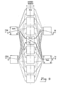
- FIG. 2 An example of a 5 stage switch for 16,384 channels employing 320 switching modules is shown in Fig. 2. It can be seen that any particular path across the switch has a choice of 1 DSM for the 1st (DSMA1 to 8) and 5th (DSMC1 to 8) stages 8 DSM's for the 2nd and 4th stage (one DSM in each of the eight planes PA to PH) and 64 DSM's for the 3rd stage (any one of the eight centre DSMs in each of the eight planes).
- the full variability of the 2nd and 4th stages provides a degree of freedom not entirely essential, resulting in a blocking probability lower than necessary for practical applications.
- the prime characteristic of the 2nd and 4th stages is in giving access to all of the central (3rd stage) switching modules.
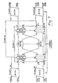
- An identical size switch shown in Fig. 3 has a very similar five stage structure, in giving this access to the central elements, but uses fixed relationships switching modules according to an embodiment of the invention for the 2nd and 4th stages. These fixed relationship modules are implemented using either a specially configured device or a variable switching module which is set to a fixed switching configuration.
- the fixed switching stages perform a "demultiplex- mix-remultiplex" operation spreading the channels on each input multiplex equally over the output multiplexes.
- the 32 channels on one input multiplex are split into 8 groups of 4 channels; one group appearing at each of the output multiplexes.
- Fig. 4 illustrates the 8 input 8 output demultiplexer-mix-remultiplexer function.
- a simple pure space-switching DMR function can be implemented using eight eight-input data multiplexors HUX1 to MUX8 and a cyclic address generator CAG as shown in Fig. 5. With such a DMR function propagation delay in the 2nd and 4th stages of a five stage switching network is eliminated. In addition control information is only required for the 1st, 3rd and 5th stages, thereby simplifying the control interface with the network.
- a basic 256 channel switching module with 8 inputs and 8 outputs, may be used in conjunction with a fixed relationships "demultiplexing-mixing-remultiplexing" device to provide the traffic handling capacity of a 5 stage structure whilst retaining the control simplicity and propagation delay associated with 3 stages.
- demultiplexing-mixing-remultiplexing device to provide the traffic handling capacity of a 5 stage structure whilst retaining the control simplicity and propagation delay associated with 3 stages.
- a switch structure may be composed of many different numbers of stages and mixes of controlled switching modules and fixed relationships DMR modules, each providing varying characteristics in terms of, capacity of traffic handled, control complexity, propagation delay, grade of service and freedom of traffic flow.
- DMR modules fixed relationships
- n>o 4n + 1 total stages
- switch structures similar to the example described above in which there are 4n + 1 total stages (n>o) composed of alternate switching modules and DMR elements. These can be designed to allow full freedom of traffic flow with only 2n + 1 controlled stages.
- the switch traffic handling capacity can be increased by use of larger switching modules or DMR elements, while the converse holds for a decrease in size.
- One method of doubling the capacity of a basic 256 channel switching module is shown in Fig. 6.
- DMR function is derived below by means of an example for use where the majority of paths through the switch will be duplex as in a telecommunications application.
- FIG. 8 shows how the overall path correlation can be applied for a forward path AB and a return path BA for a 5 stage switch.
- the input and output stages can be composed of DSMs arranged in square arrays to provide the larger sizes of switch.
- the central stages are really 3 stages internally DMR-DSM-DMR, again with the DSM organised in square arrays for the larger switch sizes. In order to make the connection AB, then all the central stages are inspected to find one which has both paths AL and LB free.
- time slot y will be used on the route to B and from the DSM on plane p to the DMR input. It is sensible to confine the input DMRs and output DMRs to have the same switching function.
- time slot t used for passage through the DMR can be expressed as:- where i is the physical input route and o is the physical output route. For each combination of i and o values there will be a choice of 4 time slots. To find a forward path through the inner stages it is necessary to locate a central DSM plane p which has both time slots x and y free. Thus the search is restricted to 4 input slots and 4 associated output time slots for each of the 8 DSM planes.
- the return delay dBA in time slots is given by,
- each stage will also have a real propagation delay which must be added. Since cancellation of this delay does not occur the loop delay is 3 frames plus 2 times the propagation delay in one direction.
- This function may be represented by a matrix.
- An example of such a DMR function is shown in Fig. 10.
- the references A-H are the time slot range over which an input is connected to an output.
- One possible allocation of A to H is as follows:-
- Custom LSI aligner circuits can greatly simplify intermodule communications offering automatic compensation over a wide range of separation. Splitting a 2.048Mb/s FCM/TDM link into four 512 Kb/s transfer interface lines TIl-4 would accommodate a nominal + 976 nano-second delay variation between input and output timing clock ITC and OTC as shown in Fig. 11. Generally other transmission rates may be used as required. Direct implementation would be inefficient in the use of links. It is possible to locate the demultiplexing and multiplexing circuitry at the receive module, providing timing information is transmitted along with the data link. A particular implementation is shown in Fig. 12. The transmit bit clock TXCLK is used to strobe information from the incoming p.c.m.
- Switches which make use of a DMR function can benefit from the integration of both retiming and the demultiplex- mix-remultiplex operations into a single large scale integration device.
- An example of an 8 x 8 DMR with integral retiming is shown in Fig. 14 consisting of eight retimer circuits RT1-8 (each of which is similar to the circuit of Fig. 12) and eight output multiplexers NUXl-8.
- the clock inputs to the retiming circuits RT1-8 consist of the transmit time base (TX F S and TXCLK) and the receive time base (RXFS and RXCLK) and they may be commoned up as required. In such cases common timebase generators can be used. In most applications only one output timing reference RXCLK will be necessary and this can also drive the cyclic address generator CAG for the DMR function.
- the improved tolerance on the output timing can be achieved by placing the output binary of retiming circuit after the DMR multiplexor.
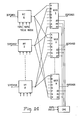
- FIG. 16 A method of fragmenting this structure down into discrete modules is shown in Fig. 16. Since the outer stage module consists of 4 switching planes of 16 x 16 for both the receiving and transmitting stage, a maximum of 32 outer modules can be equipped. The central module consists of 4 super planes of 128 x 128 central stage and thus 4 replicas exist. From Fig. 16 it can be seen that 16 pcm/TDM links (32 chan) at 2.048 Mb/s are connected from any one outer module to any one central module. For transmission purposes the PCM/TDM links may be multiplexed up to 4.096 MD/s, thus reducing the interconnection requirements to 8 data links plus 2 clocks for strobing and retiming. Where balanced line communication is used a 10 pair cable will be sufficient.
- FIG. 17 An example of a device which embodies all the functions of DMR, retiming and control signalling is shown in Fig. 17.
- This particular device has 8 data inputs ICPCMSl-8 subdivided into two groups of 4, each with their own input timing reference clocks ICLKA and ICLKB and 8 data outputs OGPCMSl-8 with a common timing reference OGTB.
- Both input frame synchronisation signals TXFSA and TXFSB are retimed to allow information to be embedded on the remaining non synchronisation timeslots.
- the device also has two control inputs CO and Cl for the DMR function allowing four configurations:-
- Fig. 18 illustrates the DMR options provided in which A-H is the time slot range over which an input is connected to an output.
- A-H is the time slot range over which an input is connected to an output.
- the allocation of A to H being the same as that defined above in relation to Fig. 10.
Landscapes
- Engineering & Computer Science (AREA)
- Computer Networks & Wireless Communication (AREA)
- Use Of Switch Circuits For Exchanges And Methods Of Control Of Multiplex Exchanges (AREA)
- Data Exchanges In Wide-Area Networks (AREA)
Applications Claiming Priority (2)
| Application Number | Priority Date | Filing Date | Title |
|---|---|---|---|
| GB8013555 | 1980-04-24 | ||
| GB8013555A GB2074815B (en) | 1980-04-24 | 1980-04-24 | Telecommunications switching network using digital switching modules |
Publications (2)
| Publication Number | Publication Date |
|---|---|
| EP0039134A1 true EP0039134A1 (fr) | 1981-11-04 |
| EP0039134B1 EP0039134B1 (fr) | 1984-02-15 |
Family
ID=10512984
Family Applications (1)
| Application Number | Title | Priority Date | Filing Date |
|---|---|---|---|
| EP81301281A Expired EP0039134B1 (fr) | 1980-04-24 | 1981-03-25 | Réseau de commutation utilisant des modules de commutation numérique |
Country Status (10)
| Country | Link |
|---|---|
| US (1) | US4425640A (fr) |
| EP (1) | EP0039134B1 (fr) |
| DE (1) | DE3162215D1 (fr) |
| GB (1) | GB2074815B (fr) |
| HK (1) | HK78085A (fr) |
| IE (1) | IE52018B1 (fr) |
| NZ (1) | NZ196908A (fr) |
| PT (1) | PT72869B (fr) |
| SG (1) | SG29485G (fr) |
| ZA (1) | ZA812079B (fr) |
Cited By (4)
| Publication number | Priority date | Publication date | Assignee | Title |
|---|---|---|---|---|
| EP0056600A3 (en) * | 1981-01-15 | 1982-08-11 | Cselt Centro Studi E Laboratori Telecomunicazioni S.P.A. | Modular structure of pcm-switched distributed control and distributed-diagnostic network |
| EP0116386B1 (fr) * | 1983-01-27 | 1986-11-05 | Koninklijke Philips Electronics N.V. | Système de commutation à multiplexage temporel |
| EP0317055A3 (en) * | 1987-11-13 | 1990-03-14 | The Plessey Company Plc | Telecommunications digital switch |
| EP0411742A3 (en) * | 1989-08-03 | 1992-04-22 | Gec Plessey Telecommunications Limited | Message switching arrangements |
Families Citing this family (73)
| Publication number | Priority date | Publication date | Assignee | Title |
|---|---|---|---|---|
| US4597075A (en) * | 1981-08-21 | 1986-06-24 | Italtel-Societa Italiana Telecomunicazioni S.P.A. | Modular switching network for telecommunication system |
| FR2513471A1 (fr) * | 1981-09-18 | 1983-03-25 | Cit Alcatel | Dispositif de distribution de signaux pour autocommutateur temporel |
| GB2120041B (en) * | 1982-04-24 | 1985-10-02 | Plessey Co Plc | Digital switching network for telecommunications exchange |
| GB2130049B (en) * | 1982-10-21 | 1986-01-29 | Plessey Co Plc | Method of growth of a digital switchblock |
| GB2153634B (en) * | 1984-02-02 | 1987-03-25 | Plessey Co Plc | An arrangement for controlling switched speech or data communication in a communications exchange |
| US5293489A (en) * | 1985-01-24 | 1994-03-08 | Nec Corporation | Circuit arrangement capable of centralizing control of a switching network |
| EP0212431B1 (fr) * | 1985-08-12 | 1989-11-08 | Politechnika Poznanska | Réseau de commutation numérique à plusieurs étages |
| EP0238712A1 (fr) * | 1986-01-27 | 1987-09-30 | Siemens-Albis Aktiengesellschaft | Matrice de commutateur commandée |
| US4730305A (en) * | 1986-04-11 | 1988-03-08 | American Telephone And Telegraph Company, At&T Bell Laboratories | Fast assignment technique for use in a switching arrangement |
| US4821034A (en) * | 1987-02-06 | 1989-04-11 | Ancor Communications, Inc. | Digital exchange switch element and network |
| US4991169A (en) * | 1988-08-02 | 1991-02-05 | International Business Machines Corporation | Real-time digital signal processing relative to multiple digital communication channels |
| DE8905982U1 (de) * | 1989-05-12 | 1989-07-13 | Siemens AG, 1000 Berlin und 8000 München | Mehrstufige Koppeleinrichtung |
| US5528406A (en) * | 1991-08-02 | 1996-06-18 | Gpt Limited | Telecommunications switching device |
| GB9317897D0 (en) * | 1993-08-27 | 1993-10-13 | Plessey Telecomm | Telecommunications switching element |
| GB9614489D0 (en) * | 1996-07-10 | 1996-09-04 | Plessey Telecomm | Telecommunication networks |
| US6697359B1 (en) * | 1999-07-02 | 2004-02-24 | Ancor Communications, Inc. | High performance switch fabric element and switch systems |
| CA2283953C (fr) | 1999-09-27 | 2009-07-28 | Nortel Networks Corporation | Commutateur compact a grande capacite |
| JP2003516657A (ja) * | 1999-12-10 | 2003-05-13 | キューロジック スウィッチ プロダクツ,インコーポレイティド | ファイバチャネル・クレジット・エクステンダ及び中継器 |
| WO2001095566A2 (fr) * | 2000-06-05 | 2001-12-13 | Qlogic Switch Products, Inc. | Zonage au niveau d'une boucle, renforce par du materiel, pour matrice de commutation de canaux de fibres optiques |
| US7978695B2 (en) * | 2000-06-05 | 2011-07-12 | Qlogic Switch Products, Inc. | Hardware-enforced loop and NPIV hard zoning for fibre channel switch fabric |
| US7233590B2 (en) * | 2001-07-06 | 2007-06-19 | Nortel Networks Limited | Switched channel-band network |
| AU2003225284A1 (en) * | 2002-05-02 | 2003-11-17 | Ciena Corporation | Distribution stage for enabling efficient expansion of a switching network |
| US7154886B2 (en) * | 2002-07-22 | 2006-12-26 | Qlogic Corporation | Method and system for primary blade selection in a multi-module fiber channel switch |
| US7230929B2 (en) * | 2002-07-22 | 2007-06-12 | Qlogic, Corporation | Method and system for dynamically assigning domain identification in a multi-module fibre channel switch |
| US7334046B1 (en) | 2002-08-05 | 2008-02-19 | Qlogic, Corporation | System and method for optimizing frame routing in a network |
| US7397768B1 (en) | 2002-09-11 | 2008-07-08 | Qlogic, Corporation | Zone management in a multi-module fibre channel switch |
| US7362717B1 (en) | 2002-10-03 | 2008-04-22 | Qlogic, Corporation | Method and system for using distributed name servers in multi-module fibre channel switches |
| US6886141B1 (en) | 2002-10-07 | 2005-04-26 | Qlogic Corporation | Method and system for reducing congestion in computer networks |
| US7319669B1 (en) | 2002-11-22 | 2008-01-15 | Qlogic, Corporation | Method and system for controlling packet flow in networks |
| US7620059B2 (en) * | 2003-07-16 | 2009-11-17 | Qlogic, Corporation | Method and apparatus for accelerating receive-modify-send frames in a fibre channel network |
| US7355966B2 (en) * | 2003-07-16 | 2008-04-08 | Qlogic, Corporation | Method and system for minimizing disruption in common-access networks |
| US7453802B2 (en) * | 2003-07-16 | 2008-11-18 | Qlogic, Corporation | Method and apparatus for detecting and removing orphaned primitives in a fibre channel network |
| US7471635B2 (en) | 2003-07-16 | 2008-12-30 | Qlogic, Corporation | Method and apparatus for test pattern generation |
| US7525910B2 (en) * | 2003-07-16 | 2009-04-28 | Qlogic, Corporation | Method and system for non-disruptive data capture in networks |
| US7463646B2 (en) * | 2003-07-16 | 2008-12-09 | Qlogic Corporation | Method and system for fibre channel arbitrated loop acceleration |
| US7388843B2 (en) * | 2003-07-16 | 2008-06-17 | Qlogic, Corporation | Method and apparatus for testing loop pathway integrity in a fibre channel arbitrated loop |
| US7152132B2 (en) * | 2003-07-16 | 2006-12-19 | Qlogic Corporation | Method and apparatus for improving buffer utilization in communication networks |
| US7646767B2 (en) | 2003-07-21 | 2010-01-12 | Qlogic, Corporation | Method and system for programmable data dependant network routing |
| US7630384B2 (en) * | 2003-07-21 | 2009-12-08 | Qlogic, Corporation | Method and system for distributing credit in fibre channel systems |
| US7512067B2 (en) * | 2003-07-21 | 2009-03-31 | Qlogic, Corporation | Method and system for congestion control based on optimum bandwidth allocation in a fibre channel switch |
| US7466700B2 (en) * | 2003-07-21 | 2008-12-16 | Qlogic, Corporation | LUN based hard zoning in fibre channel switches |
| US7792115B2 (en) * | 2003-07-21 | 2010-09-07 | Qlogic, Corporation | Method and system for routing and filtering network data packets in fibre channel systems |
| US7583597B2 (en) * | 2003-07-21 | 2009-09-01 | Qlogic Corporation | Method and system for improving bandwidth and reducing idles in fibre channel switches |
| US7558281B2 (en) * | 2003-07-21 | 2009-07-07 | Qlogic, Corporation | Method and system for configuring fibre channel ports |
| US7447224B2 (en) * | 2003-07-21 | 2008-11-04 | Qlogic, Corporation | Method and system for routing fibre channel frames |
| US7684401B2 (en) * | 2003-07-21 | 2010-03-23 | Qlogic, Corporation | Method and system for using extended fabric features with fibre channel switch elements |
| US7525983B2 (en) * | 2003-07-21 | 2009-04-28 | Qlogic, Corporation | Method and system for selecting virtual lanes in fibre channel switches |
| US7420982B2 (en) * | 2003-07-21 | 2008-09-02 | Qlogic, Corporation | Method and system for keeping a fibre channel arbitrated loop open during frame gaps |
| US7894348B2 (en) * | 2003-07-21 | 2011-02-22 | Qlogic, Corporation | Method and system for congestion control in a fibre channel switch |
| US7573909B2 (en) * | 2003-07-21 | 2009-08-11 | Qlogic, Corporation | Method and system for programmable data dependant network routing |
| US7580354B2 (en) * | 2003-07-21 | 2009-08-25 | Qlogic, Corporation | Multi-speed cut through operation in fibre channel switches |
| US7430175B2 (en) * | 2003-07-21 | 2008-09-30 | Qlogic, Corporation | Method and system for managing traffic in fibre channel systems |
| US7477655B2 (en) * | 2003-07-21 | 2009-01-13 | Qlogic, Corporation | Method and system for power control of fibre channel switches |
| US7522529B2 (en) * | 2003-07-21 | 2009-04-21 | Qlogic, Corporation | Method and system for detecting congestion and over subscription in a fibre channel network |
| US7406092B2 (en) * | 2003-07-21 | 2008-07-29 | Qlogic, Corporation | Programmable pseudo virtual lanes for fibre channel systems |
| US7522522B2 (en) * | 2003-07-21 | 2009-04-21 | Qlogic, Corporation | Method and system for reducing latency and congestion in fibre channel switches |
| US7352701B1 (en) | 2003-09-19 | 2008-04-01 | Qlogic, Corporation | Buffer to buffer credit recovery for in-line fibre channel credit extension devices |
| US7103504B1 (en) | 2003-11-21 | 2006-09-05 | Qlogic Corporation | Method and system for monitoring events in storage area networks |
| US7564789B2 (en) * | 2004-02-05 | 2009-07-21 | Qlogic, Corporation | Method and system for reducing deadlock in fibre channel fabrics using virtual lanes |
| US7480293B2 (en) * | 2004-02-05 | 2009-01-20 | Qlogic, Corporation | Method and system for preventing deadlock in fibre channel fabrics using frame priorities |
| US7930377B2 (en) * | 2004-04-23 | 2011-04-19 | Qlogic, Corporation | Method and system for using boot servers in networks |
| US7340167B2 (en) * | 2004-04-23 | 2008-03-04 | Qlogic, Corporation | Fibre channel transparent switch for mixed switch fabrics |
| US7669190B2 (en) | 2004-05-18 | 2010-02-23 | Qlogic, Corporation | Method and system for efficiently recording processor events in host bus adapters |
| US7404020B2 (en) * | 2004-07-20 | 2008-07-22 | Qlogic, Corporation | Integrated fibre channel fabric controller |
| US8295299B2 (en) * | 2004-10-01 | 2012-10-23 | Qlogic, Corporation | High speed fibre channel switch element |
| US7380030B2 (en) * | 2004-10-01 | 2008-05-27 | Qlogic, Corp. | Method and system for using an in-line credit extender with a host bus adapter |
| US7593997B2 (en) | 2004-10-01 | 2009-09-22 | Qlogic, Corporation | Method and system for LUN remapping in fibre channel networks |
| US7411958B2 (en) | 2004-10-01 | 2008-08-12 | Qlogic, Corporation | Method and system for transferring data directly between storage devices in a storage area network |
| US7676611B2 (en) * | 2004-10-01 | 2010-03-09 | Qlogic, Corporation | Method and system for processing out of orders frames |
| US7519058B2 (en) * | 2005-01-18 | 2009-04-14 | Qlogic, Corporation | Address translation in fibre channel switches |
| US8464238B1 (en) | 2006-01-31 | 2013-06-11 | Qlogic, Corporation | Method and system for managing storage area networks |
| US7548560B1 (en) | 2006-02-27 | 2009-06-16 | Qlogic, Corporation | Method and system for checking frame-length in fibre channel frames |
| US7613816B1 (en) | 2006-11-15 | 2009-11-03 | Qlogic, Corporation | Method and system for routing network information |
Citations (5)
| Publication number | Priority date | Publication date | Assignee | Title |
|---|---|---|---|---|
| US3740480A (en) * | 1971-12-27 | 1973-06-19 | Bell Telephone Labor Inc | Time division multiplex switching system utilizing all time division techniques |
| FR2331929A1 (fr) * | 1975-11-17 | 1977-06-10 | Nippon Telegraph & Telephone | Reseaux de communication a plusieurs etages utilises dans un systeme de commutation de telecommunications |
| US4093827A (en) * | 1976-02-17 | 1978-06-06 | Thomson-Csf | Symmetrical time division matrix and a network equipped with this kind of matrix |
| GB2014018A (en) * | 1978-02-01 | 1979-08-15 | Nippon Telegraph & Telephone | Time division telephone switching systems |
| DE2836695A1 (de) * | 1978-08-22 | 1980-03-06 | Siemens Ag | Digitalsignal-vermittlungssystem |
Family Cites Families (3)
| Publication number | Priority date | Publication date | Assignee | Title |
|---|---|---|---|---|
| US4201891A (en) | 1978-03-17 | 1980-05-06 | International Telephone And Telegraph Corporation | Expandable digital switching network |
| CA1065977A (fr) | 1977-05-09 | 1979-11-06 | Real Gagnier | Reseau de commutation pour reseau pcm tdm |
| JPS5555693A (en) | 1978-10-19 | 1980-04-23 | Nippon Telegr & Teleph Corp <Ntt> | Time sharing exchanging circuit |
-
1980
- 1980-04-24 GB GB8013555A patent/GB2074815B/en not_active Expired
-
1981
- 1981-03-25 DE DE8181301281T patent/DE3162215D1/de not_active Expired
- 1981-03-25 EP EP81301281A patent/EP0039134B1/fr not_active Expired
- 1981-03-27 ZA ZA00812079A patent/ZA812079B/xx unknown
- 1981-04-15 PT PT72869A patent/PT72869B/pt not_active IP Right Cessation
- 1981-04-20 US US06/255,487 patent/US4425640A/en not_active Expired - Lifetime
- 1981-04-23 IE IE915/81A patent/IE52018B1/en not_active IP Right Cessation
- 1981-04-23 NZ NZ196908A patent/NZ196908A/en unknown
-
1985
- 1985-04-23 SG SG294/85A patent/SG29485G/en unknown
- 1985-10-10 HK HK780/85A patent/HK78085A/xx not_active IP Right Cessation
Patent Citations (5)
| Publication number | Priority date | Publication date | Assignee | Title |
|---|---|---|---|---|
| US3740480A (en) * | 1971-12-27 | 1973-06-19 | Bell Telephone Labor Inc | Time division multiplex switching system utilizing all time division techniques |
| FR2331929A1 (fr) * | 1975-11-17 | 1977-06-10 | Nippon Telegraph & Telephone | Reseaux de communication a plusieurs etages utilises dans un systeme de commutation de telecommunications |
| US4093827A (en) * | 1976-02-17 | 1978-06-06 | Thomson-Csf | Symmetrical time division matrix and a network equipped with this kind of matrix |
| GB2014018A (en) * | 1978-02-01 | 1979-08-15 | Nippon Telegraph & Telephone | Time division telephone switching systems |
| DE2836695A1 (de) * | 1978-08-22 | 1980-03-06 | Siemens Ag | Digitalsignal-vermittlungssystem |
Non-Patent Citations (4)
| Title |
|---|
| Colloque International de Commutation International Switching Symposium, 7-11th May, 1979, Paris (FR) J. HAURI et al.: "Use of LSI Circuits in the MT Digital Switching Family", pages 648-654 * pages 653, 654, paragraph: "Branches du reseau" * * |
| Commutation et Electronique, No. 50, July 1975, Paris (FR) M. REVEL et al.: "Brasseur de Voies Entre Liaisons Numeriques TN 1", pages 7-17 * page 11, paragraph 3.1; pages 16 and 17, paragraph 7.2 * * |
| International Zurich Seminar on Digital Communications, 9-11yh March, 1976, Zurich (CH) H. PFANNSCHMIDY.: "Limitation of Transmission Rate in High-Speed TDM-Switching Networks Using Schottky-TTL Circuit Technology", pages C3.1 to C3.6 * pages C3.3 and C3.4, paragraph 4.1 * * |
| Review of the Electrical Communication Laboratories, Vol. 27, No. 9-10, September-October 1979, Tokyo (JP) GOTOH et al.: "DTS-1 DIGITAL Telephone System for a Large Toll Office", pages 702-713 * page 707, left-hand column, lines 23-27 * * |
Cited By (5)
| Publication number | Priority date | Publication date | Assignee | Title |
|---|---|---|---|---|
| EP0056600A3 (en) * | 1981-01-15 | 1982-08-11 | Cselt Centro Studi E Laboratori Telecomunicazioni S.P.A. | Modular structure of pcm-switched distributed control and distributed-diagnostic network |
| EP0116386B1 (fr) * | 1983-01-27 | 1986-11-05 | Koninklijke Philips Electronics N.V. | Système de commutation à multiplexage temporel |
| EP0317055A3 (en) * | 1987-11-13 | 1990-03-14 | The Plessey Company Plc | Telecommunications digital switch |
| AU608659B2 (en) * | 1987-11-13 | 1991-04-11 | Gec Plessey Telecommunications Limited | Telecommunications digital switch |
| EP0411742A3 (en) * | 1989-08-03 | 1992-04-22 | Gec Plessey Telecommunications Limited | Message switching arrangements |
Also Published As
| Publication number | Publication date |
|---|---|
| DE3162215D1 (en) | 1984-03-22 |
| EP0039134B1 (fr) | 1984-02-15 |
| IE52018B1 (en) | 1987-05-27 |
| GB2074815B (en) | 1984-06-27 |
| PT72869B (en) | 1982-06-01 |
| ZA812079B (en) | 1982-04-28 |
| NZ196908A (en) | 1985-04-30 |
| HK78085A (en) | 1985-10-18 |
| IE810915L (en) | 1981-10-24 |
| PT72869A (en) | 1981-05-01 |
| SG29485G (en) | 1985-11-15 |
| US4425640A (en) | 1984-01-10 |
| GB2074815A (en) | 1981-11-04 |
Similar Documents
| Publication | Publication Date | Title |
|---|---|---|
| EP0039134B1 (fr) | Réseau de commutation utilisant des modules de commutation numérique | |
| US4685101A (en) | Digital multiplexer for PCM voice channels having a cross-connect capability | |
| US5784369A (en) | Methods and system for switching time-division-multiplexed digital signals of different rates | |
| US5200746A (en) | Switching module for digital cross-connect systems | |
| US4400627A (en) | Telephone switching network | |
| US5757806A (en) | Data multiplexing system having at least one low-speed interface circuit connected to a bus | |
| US5519702A (en) | Digital communication system | |
| EP0317055B1 (fr) | Champs de couplage numérique pour télécommunications | |
| SE456793B (sv) | Digitaltelekommunkationssystem foer faelt med digitalt kodade data i ett flertal kanaler | |
| US4680752A (en) | Time switch in a time division switching network | |
| US4601029A (en) | Communication switching system | |
| EP0542741A4 (fr) | Echangeurs de tranche de temps de matrices serielles. | |
| US4025725A (en) | Telecommunication switching network having a multistage reversed trunking scheme and switching on a four wire basis | |
| CA1083696A (fr) | Reseau de commutation par partage du temps | |
| Charransol et al. | Development of a time-division switching network usable in a very large range of capacities | |
| JPH02257796A (ja) | 伝送ネットワーク | |
| US6366579B1 (en) | Modular time-space switch | |
| US4399534A (en) | Dual rail time and control unit for a duplex T-S-T-digital switching system | |
| JPH02305132A (ja) | フレキシブルマルチプレクサ | |
| US4399369A (en) | Dual rail time and control unit for a duplex T-S-T-digital switching system | |
| US4524442A (en) | Modularly expandable space stage for a T-S-T digital switching system | |
| US4406005A (en) | Dual rail time control unit for a T-S-T-digital switching system | |
| AU700164B2 (en) | Three stage switching unit | |
| JPS5866489A (ja) | 光時間スイツチ | |
| US4392223A (en) | Dual rail time and control unit for a T-S-T-digital switching system |
Legal Events
| Date | Code | Title | Description |
|---|---|---|---|
| PUAI | Public reference made under article 153(3) epc to a published international application that has entered the european phase |
Free format text: ORIGINAL CODE: 0009012 |
|
| AK | Designated contracting states |
Designated state(s): DE FR IT NL SE |
|
| 17P | Request for examination filed |
Effective date: 19811014 |
|
| RAP1 | Party data changed (applicant data changed or rights of an application transferred) |
Owner name: THE PLESSEY COMPANY PLC |
|
| ITF | It: translation for a ep patent filed | ||
| GRAA | (expected) grant |
Free format text: ORIGINAL CODE: 0009210 |
|
| AK | Designated contracting states |
Designated state(s): DE FR IT NL SE |
|
| ET | Fr: translation filed | ||
| REF | Corresponds to: |
Ref document number: 3162215 Country of ref document: DE Date of ref document: 19840322 |
|
| PLBE | No opposition filed within time limit |
Free format text: ORIGINAL CODE: 0009261 |
|
| STAA | Information on the status of an ep patent application or granted ep patent |
Free format text: STATUS: NO OPPOSITION FILED WITHIN TIME LIMIT |
|
| 26N | No opposition filed | ||
| REG | Reference to a national code |
Ref country code: GB Ref legal event code: 732 |
|
| REG | Reference to a national code |
Ref country code: GB Ref legal event code: 732 |
|
| ITPR | It: changes in ownership of a european patent |
Owner name: CESSIONE;GEC PLESSEY TELECOMUNICATIONS LIMITED |
|
| ITTA | It: last paid annual fee | ||
| REG | Reference to a national code |
Ref country code: FR Ref legal event code: TP |
|
| PGFP | Annual fee paid to national office [announced via postgrant information from national office to epo] |
Ref country code: NL Payment date: 19920331 Year of fee payment: 12 |
|
| PG25 | Lapsed in a contracting state [announced via postgrant information from national office to epo] |
Ref country code: NL Effective date: 19931001 |
|
| NLV4 | Nl: lapsed or anulled due to non-payment of the annual fee | ||
| PGFP | Annual fee paid to national office [announced via postgrant information from national office to epo] |
Ref country code: SE Payment date: 19940415 Year of fee payment: 14 |
|
| EAL | Se: european patent in force in sweden |
Ref document number: 81301281.2 |
|
| PG25 | Lapsed in a contracting state [announced via postgrant information from national office to epo] |
Ref country code: SE Effective date: 19950326 |
|
| EUG | Se: european patent has lapsed |
Ref document number: 81301281.2 |
|
| PGFP | Annual fee paid to national office [announced via postgrant information from national office to epo] |
Ref country code: FR Payment date: 19990309 Year of fee payment: 19 |
|
| PGFP | Annual fee paid to national office [announced via postgrant information from national office to epo] |
Ref country code: DE Payment date: 19990406 Year of fee payment: 19 |
|
| PG25 | Lapsed in a contracting state [announced via postgrant information from national office to epo] |
Ref country code: FR Free format text: LAPSE BECAUSE OF NON-PAYMENT OF DUE FEES Effective date: 20001130 |
|
| REG | Reference to a national code |
Ref country code: FR Ref legal event code: ST |
|
| PG25 | Lapsed in a contracting state [announced via postgrant information from national office to epo] |
Ref country code: DE Free format text: LAPSE BECAUSE OF NON-PAYMENT OF DUE FEES Effective date: 20010103 |