EP0039449A1 - Dispositif pour la régénération d'une mémoire non volatile - Google Patents
Dispositif pour la régénération d'une mémoire non volatile Download PDFInfo
- Publication number
- EP0039449A1 EP0039449A1 EP81103068A EP81103068A EP0039449A1 EP 0039449 A1 EP0039449 A1 EP 0039449A1 EP 81103068 A EP81103068 A EP 81103068A EP 81103068 A EP81103068 A EP 81103068A EP 0039449 A1 EP0039449 A1 EP 0039449A1
- Authority
- EP
- European Patent Office
- Prior art keywords
- refreshing
- memory
- address
- volatile
- read out
- Prior art date
- Legal status (The legal status is an assumption and is not a legal conclusion. Google has not performed a legal analysis and makes no representation as to the accuracy of the status listed.)
- Granted
Links
Images


Classifications
-
- G—PHYSICS
- G11—INFORMATION STORAGE
- G11C—STATIC STORES
- G11C16/00—Erasable programmable read-only memories
- G11C16/02—Erasable programmable read-only memories electrically programmable
- G11C16/06—Auxiliary circuits, e.g. for writing into memory
- G11C16/26—Sensing or reading circuits; Data output circuits
-
- G—PHYSICS
- G06—COMPUTING OR CALCULATING; COUNTING
- G06F—ELECTRIC DIGITAL DATA PROCESSING
- G06F11/00—Error detection; Error correction; Monitoring
- G06F11/07—Responding to the occurrence of a fault, e.g. fault tolerance
- G06F11/14—Error detection or correction of the data by redundancy in operations
- G06F11/1402—Saving, restoring, recovering or retrying
-
- G—PHYSICS
- G11—INFORMATION STORAGE
- G11C—STATIC STORES
- G11C16/00—Erasable programmable read-only memories
- G11C16/02—Erasable programmable read-only memories electrically programmable
- G11C16/06—Auxiliary circuits, e.g. for writing into memory
- G11C16/34—Determination of programming status, e.g. threshold voltage, overprogramming or underprogramming, retention
- G11C16/3418—Disturbance prevention or evaluation; Refreshing of disturbed memory data
- G11C16/3431—Circuits or methods to detect disturbed nonvolatile memory cells, e.g. which still read as programmed but with threshold less than the program verify threshold or read as erased but with threshold greater than the erase verify threshold, and to reverse the disturbance via a refreshing programming or erasing step
Definitions
- This invention relates to an apparatus and method of refreshing non-volatile memories such as MNOS (Metal Nitride Oxide Semiconductor) memory, and it is to present, even in the case of stoppage of power supply during the refreshing action, a refreshing scheme which has no fear that the contents of the memory are erased or disturbed.
- MNOS Metal Nitride Oxide Semiconductor
- a data signal of an address to be refreshed (hereinafter this address is called as a refreshing address) is read out from this address and it is stored once in a data register comprizing such as a shift register, then as a next step all the contents of this refreshing address is erased and thereafter the data signal, which has been stored in the data register, is rewritten into this refreshing address.
- the data register used is a volatile memory, if the power supply is shut off during the processes after the erasion process until the rewriting process, the contents of the data register is all erased, accordingly the data signal of the refreshing address is all lost forever or is lost partly, giving falsely converted data.
- This invention purports to remove the drawbacks hitherto existed in the conventional apparatus and methods for refreshing scheme for non-volatile memory, and to present a new apparatus and methos for refreshing it, which can protect the contents of the memory even when its power supply is shut off during its refreshing action and can be realized by a relatively simple means without using a bulky capacitor.
- the apparatus and method for refreshing non-volatile memory in accordance with the present invention is devised in a manner that in any step of its refreshing routine the data signal is always held in a refreshing address or in a refreshing buffer memory which is prepared in this non-volatile memory device. Therefore even in the case of stoppage of power supply during the course of the refreshing action, it is assured that the data signal is held in the refreshing buffer memory.
- address data representing that at which refreshing address the present data signal has been held and status data representing that in which step of the refreshing routine the refreshing action has been interrupted due to the stoppage of the power supply are also stored in a part of this non-volatile memory device.
- the refreshing operation can be started from the step of the refreshing routine, which was on the way of refreshing at the preceding ' chance of the device operation, and thus the whole refreshing routine can be completed any time.
- FIG. 1 which shows the whole of the memory device in accordance with the refreshing scheme of the present invention is shown as a black diagram
- 1 is a memory circuit
- 2 is its controlling circuit.
- the memory circuit 1 comprises mainly an MNOS memory 3 having a memory size of as much as 16 addresses of 16 bit unit memory cell.
- An address of the memory 3 which is to be read out or written in is designated by an address register 5 through an address driver 4, and the contents of that address is read out to or written in from a data register 7 through an input-output circuit 6.
- the data register 7 comprises mainly a 16 bit shift register. Both the address register 5 and the data register 7 operate in several operating modes and those operation modes are changed over by a mode decoder 8 and a mode register 9 in accordance with a mode signal issued from the external control circuit 2.
- Those signals designating these operating modes are transmitted together with various data signals from the control circuit 2 through data line. Distinction between the data signals and the mode-designating signals is carried out by sending switch-over signals through a separate switch-over signal line (not shown in the diagram). Also a shift clock necessary for these operations is supplied from the control circuit 2 through a clock line (not shown in the diagram).
- 10 is an input-output circuit (interface circuit) through which those various signals described above are transferred to and from the control circuit 2.
- control circuit 2 comprises mainly a microcomputer 11 which controls the memory circuit 1 in a manner described below and an instruction ROM 12 storing a program for instructing the operation of the microcomputer 11.
- the memory area of the MNOS memory 3 is divided into three firstly “0”, secondly “F”, and thirdly “1", “2", “3", “4", "5", “6", “7”, “8", “9", "A", "B", “C”, “D” and “E”, as shown in FIG. 2.
- the address is referred to by using the quotation marks, for example "0"
- an address signal stored in that address, (i.e., contents of that address or data) to represent the address is referred to without such quotation mark, for example 0.
- the first one of the memory area of the MNOS memory 3, that is, the memory area of address "0" is used as a buffer memory for storing temporalily the data signal of an address whose contents are to be refreshed during the refreshing operation.
- the second one that is, the memory area of address "F” is used both as a refreshing address memory and as a refreshing status memory.
- the refreshing address memory uses 4 bits area in the address "F” and stores a binary 4 bit refreshing address signal RA representing an address "RA” at which the refreshing operation is in progress.
- the refreshing status memory uses another 4 bit area also in the address "F” and stores a binary 4 bit refreshing status signal RS representing the statuses of the refreshing operation, that is, complete finish or half finish (details will be given later) of the refreshing action.
- the third one that is, the memory area of the remaining 14 addresses is used as a data memory area.
- An example of the data signals stored in this data memory area is, for instance, a binary coded signal representing tuning voltages of the electronic tuner of TV sets.
- a binary coded signal representing tuning voltages of the electronic tuner of TV sets.
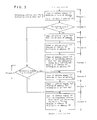
- the refreshing routine When the refreshing routine is called from a main routine, first the address signal of the address "F" is issued from the control circuit 2 to the memory circuit 1. This address signal is written in the address register 5, therefore the address "F” of the MNOS memory 3 is designated, that is, the refreshing address memory and refreshing status memory are designated. Then from this address "F” the refreshing address signal RA and the refreshing status signal RS are read out to the data register 27 and they are sent out to the control circuit 2 through a data line 72.
- the microcomputer 11 discriminates whether the refreshing status signal RS indicates a specific coded signal representing the status of finishing all the necessary refreshing action at a certain address (specific coded signal in this case is, hereinafter, called as finish signal) or indicates non-specific coded signal.
- specific coded signal in this case is, hereinafter, called as finish signal
- non-specific coded signal namely in the case other than the finish signal
- another specific coded signal representing the status of half-finish that is, the status of finish only to a halfway of necessary action
- specific coded signal in this case is, hereinafter, called as half-finish signal
- the refreshing address signal RA which was read out to the control circuit 2 also in the preceding operation is now converted into 16 bit serial signal from a binary 4 bit parallel signal in the control circuit 2 and issued to the memory circuit 1 and written into the address register 5, thereby an address "RA" in the MNOS memory 3 is designated.
- This address "RA” can be any one of the data memory area, "1" to "E", of the MNOS memory. Then a data signal stored in this address "RA" is read out to the data register 7. During this action, the data signal in the address "RA" is left without any change in that address "RA".
- the address signal "0" is issued from the control circuit 2 and it is written into the address register 5, thereby the address "0", that is, the refreshing buffer memory is designated., Then the data signal of the refreshing address "RA" which was read out to the data register 7 in the preceding process is written into this refreshing buffer memory.
- the data signal of the refreshing address "RA" can be stored in the refreshing buffer memory of the address "0".
- the refreshing action of the address "RA” is completed halfway.
- the address signal of the address "F” is issued from the control circuit 2 and it is written into the address register 5.
- the binary 4 bit refreshing address signal RA which indicates the refreshing address is under the refreshing action
- the binary 4 bit refreshing status signal RA of the half-finish signal which indicates that the refreshing action is completed halfway, are also issued from the control circuit 2 and written into the data register 7.
- the refreshing address signal RA of the address "RA” is written into the refreshing address memory, and the refreshing status signal RS of the half-finish is written into the refreshing status memory.
- the address signal of the address "0" is issued from the control circuit 2 and written into the address register 5, thereby the data signal of the refreshing address "RA" which was written in the refreshing buffer memory of the address "0" in the preceding process is read out to the data register 7. On this step, the data signal is left in the refreshing buffer memory without any change.
- the address signal of the refreshing address "RA” is issued from the control circuit 2 and written into the address register 5. Then the memory contents of this refreshing address "RA” is all erased and then the data signal formerly existed in the address "RA” is written again in the same address from the data register 7. With the above processes, the refreshing action of the refreshing address "RA” is all completed.
- the address signal of the address "F” is again issued from the control circuit 2 and written into the address register 5.
- the binary 4 bit address signal RA-1 indicating the address "RA-1" (which is the address to be refreshed next to the address "RA” of the data memory at which the refreshing action has just been completed) and the refreshing status signal RS of the finish signal indicating the completion of the refreshing action are issued from the control circuit 2 and written into the data register 7.
- the memory contents of the address "F” is erased, then from the data register 7 the refreshing address signal (RA-1) and the refreshing status signal of the finish signal are written into the refreshing address memory and the refreshing status memory, and by this process one refreshing routine is completed.
- this address signal (RA-1) indicating the refreshing address to be refreshed at the next chance of the routine operation becomes the one indicating the address "0" or the address "F"
- this address signal (RA-1) is corrected to the one indicating the address "E".
- the refreshing operation of the non-volatile memories such as the MNOS memory can be performed in accordance with the present invention.
- both the refreshing address signal RA and the refreshing status signal RS are set to the correct initial state, and hence the correct refreshing operation is assured to be executed from the next chance of the start of the refreshing routine.
- both of the finish signal and the half-finish signal are set to codes of repeated combination "1" and "0" which are the codes most scarecely met in random operations.
- the finish signal is set to "1010”
- the half-finish signal is set to "0101”.
- the data signal is still left unchanged in both the refreshing address "RA” and the refreshing buffer memory, also the half-finish signal is left in the refreshing status memory and the address signal of the refreshing address "RA" at which the refreshing operation is being in process. Therefore when the refreshing routine is started at the next chance of the resumption of the power supply, this refreshing routine is executed through the process 2 and the process 9; that is the process is executed skipping the processes 3 to 5. And then, only the latter half part of the refreshing operation namely, from the process 6 and on, is executed again, thereby a correct refreshing operation is executed.
- the execution of the refreshing routine is similar to the process 5 described before. That is, in the next chance of the refreshing operation, the routine proceeds through the process 2 and process 9, and then it is executed from the process 8. Therefore, the refreshing routine is again executed from the correct state.
- the present method does not require any bulky and expensive peripheral circuit using such as capacitors of large capacitance as in the conventional scheme and it can be performed only with the control instructed by a refreshing routine issued from a control circuit, and thereby a simple system of low cost can easily realized.
Landscapes
- Engineering & Computer Science (AREA)
- Theoretical Computer Science (AREA)
- Quality & Reliability (AREA)
- Physics & Mathematics (AREA)
- General Engineering & Computer Science (AREA)
- General Physics & Mathematics (AREA)
- Dram (AREA)
- Read Only Memory (AREA)
Applications Claiming Priority (2)
| Application Number | Priority Date | Filing Date | Title |
|---|---|---|---|
| JP55060156A JPS6022438B2 (ja) | 1980-05-06 | 1980-05-06 | 不揮発性メモリのリフレッシュ方式 |
| JP60156/80 | 1980-05-06 |
Publications (2)
| Publication Number | Publication Date |
|---|---|
| EP0039449A1 true EP0039449A1 (fr) | 1981-11-11 |
| EP0039449B1 EP0039449B1 (fr) | 1984-10-10 |
Family
ID=13133999
Family Applications (1)
| Application Number | Title | Priority Date | Filing Date |
|---|---|---|---|
| EP81103068A Expired EP0039449B1 (fr) | 1980-05-06 | 1981-04-23 | Dispositif pour la régénération d'une mémoire non volatile |
Country Status (5)
| Country | Link |
|---|---|
| US (1) | US4433395A (fr) |
| EP (1) | EP0039449B1 (fr) |
| JP (1) | JPS6022438B2 (fr) |
| CA (1) | CA1174372A (fr) |
| DE (1) | DE3166554D1 (fr) |
Cited By (3)
| Publication number | Priority date | Publication date | Assignee | Title |
|---|---|---|---|---|
| WO1987007406A1 (fr) * | 1986-05-20 | 1987-12-03 | Robert Bosch Gmbh | Procede de memorisation de donnees |
| EP0479247A1 (fr) * | 1990-10-01 | 1992-04-08 | Nec Corporation | Microordinateur avec accès à un mémorisateur externe avec temps d'attente minime |
| US5283907A (en) * | 1986-05-20 | 1994-02-01 | Robert Bosch Gmbh | Process for safeguarding transfer of data from a temporary part into a main part of a non-volatile memory |
Families Citing this family (10)
| Publication number | Priority date | Publication date | Assignee | Title |
|---|---|---|---|---|
| US4524431A (en) * | 1982-02-01 | 1985-06-18 | Texas Instruments Incorporated | High-speed nonvolatile memory array |
| US4567571A (en) * | 1982-09-07 | 1986-01-28 | Honeywell Information Systems, Inc. | Memory control for refreshing in a step mode |
| US4682292A (en) * | 1984-07-23 | 1987-07-21 | United Technologies Corporation | Fault tolerant flight data recorder |
| US4740897A (en) * | 1985-03-29 | 1988-04-26 | Panex Corporation | Memory operated well tools |
| US4866607A (en) * | 1985-05-06 | 1989-09-12 | Halliburton Company | Self-contained downhole gauge system |
| CA1242809A (fr) * | 1985-12-20 | 1988-10-04 | Mitel Corporation | Systeme de stockage de donnees |
| JPS6489099A (en) * | 1987-09-30 | 1989-04-03 | Toshiba Corp | Restorage device |
| DE50102646D1 (de) * | 2001-03-02 | 2004-07-22 | Infineon Technologies Ag | Verfahren zum einspeichern einer datenmenge in einen zielspeicherbereich und speichersystem |
| US9176800B2 (en) | 2011-08-31 | 2015-11-03 | Micron Technology, Inc. | Memory refresh methods and apparatuses |
| US10622055B2 (en) * | 2018-08-21 | 2020-04-14 | Micron Technology, Inc. | Apparatus for supplying power supply voltage to semiconductor chip including volatile memory cell |
Citations (3)
| Publication number | Priority date | Publication date | Assignee | Title |
|---|---|---|---|---|
| DE2706905A1 (de) * | 1977-02-08 | 1978-08-24 | Singer Co | Speicherschutzsystem |
| US4218764A (en) * | 1978-10-03 | 1980-08-19 | Matsushita Electric Industrial Co., Ltd. | Non-volatile memory refresh control circuit |
| EP0026980A1 (fr) * | 1979-09-04 | 1981-04-15 | Fanuc Ltd. | Procédé de ré-inscription de données dans une mémoire à bulles magnétiques à boudes majeures et mineures |
Family Cites Families (3)
| Publication number | Priority date | Publication date | Assignee | Title |
|---|---|---|---|---|
| US4145761A (en) * | 1978-03-09 | 1979-03-20 | Motorola Inc. | Ram retention during power up and power down |
| US4337524A (en) * | 1980-02-07 | 1982-06-29 | Mostek Corporation | Backup power circuit for biasing bit lines of a static semiconductor memory |
| US4323987A (en) * | 1980-03-28 | 1982-04-06 | Pitney Bowes Inc. | Power failure memory support system |
-
1980
- 1980-05-06 JP JP55060156A patent/JPS6022438B2/ja not_active Expired
-
1981
- 1981-04-23 DE DE8181103068T patent/DE3166554D1/de not_active Expired
- 1981-04-23 EP EP81103068A patent/EP0039449B1/fr not_active Expired
- 1981-04-27 US US06/257,618 patent/US4433395A/en not_active Expired - Lifetime
- 1981-05-05 CA CA000376841A patent/CA1174372A/fr not_active Expired
Patent Citations (3)
| Publication number | Priority date | Publication date | Assignee | Title |
|---|---|---|---|---|
| DE2706905A1 (de) * | 1977-02-08 | 1978-08-24 | Singer Co | Speicherschutzsystem |
| US4218764A (en) * | 1978-10-03 | 1980-08-19 | Matsushita Electric Industrial Co., Ltd. | Non-volatile memory refresh control circuit |
| EP0026980A1 (fr) * | 1979-09-04 | 1981-04-15 | Fanuc Ltd. | Procédé de ré-inscription de données dans une mémoire à bulles magnétiques à boudes majeures et mineures |
Cited By (3)
| Publication number | Priority date | Publication date | Assignee | Title |
|---|---|---|---|---|
| WO1987007406A1 (fr) * | 1986-05-20 | 1987-12-03 | Robert Bosch Gmbh | Procede de memorisation de donnees |
| US5283907A (en) * | 1986-05-20 | 1994-02-01 | Robert Bosch Gmbh | Process for safeguarding transfer of data from a temporary part into a main part of a non-volatile memory |
| EP0479247A1 (fr) * | 1990-10-01 | 1992-04-08 | Nec Corporation | Microordinateur avec accès à un mémorisateur externe avec temps d'attente minime |
Also Published As
| Publication number | Publication date |
|---|---|
| EP0039449B1 (fr) | 1984-10-10 |
| JPS6022438B2 (ja) | 1985-06-01 |
| CA1174372A (fr) | 1984-09-11 |
| DE3166554D1 (en) | 1984-11-15 |
| JPS56156988A (en) | 1981-12-03 |
| US4433395A (en) | 1984-02-21 |
Similar Documents
| Publication | Publication Date | Title |
|---|---|---|
| US4433395A (en) | Apparatus and method for refreshing non-volatile memory | |
| US6879528B2 (en) | Control method of nonvolatile memory | |
| KR100395732B1 (ko) | 반도체 기억장치 | |
| US5881002A (en) | Nonvolatile memory control circuit | |
| KR950014560B1 (ko) | 불휘발성 기억 장치 | |
| US4811294A (en) | Data integrity verifying circuit for electrically erasable and programmable read only memory (EEPROM) | |
| US6154808A (en) | Method and apparatus for controlling data erase operations of a non-volatile memory device | |
| US4877945A (en) | IC card having a function to exclude erroneous recording | |
| KR890004999B1 (ko) | 프로그램 가능 판독 전용 메모리장치 및 그를 이용한 메모리시스템 | |
| EP0398545A1 (fr) | Procédé et dispositif pour stockage de données dans une mémoire non volatile | |
| EP0288832B1 (fr) | Système d'écriture de données pour EEPROM | |
| US5724544A (en) | IC memory card utilizing dual eeproms for image and management data | |
| EP0483978B1 (fr) | Carte à circuit intégré | |
| EP0370529A2 (fr) | Micro-calculateur avec eeprom | |
| US5153854A (en) | EEPROM memory system having selectable programming voltage for low power readability | |
| US5590303A (en) | Memory designation control device | |
| JPH10124403A (ja) | ブロック消去型フラッシュメモリの書込み方法 | |
| US5247572A (en) | Apparatus for control of storing information into dial memories in a telephone set | |
| JPH05166391A (ja) | メモリ装置 | |
| JPS646600B2 (fr) | ||
| JPS6231919Y2 (fr) | ||
| EP0926601A1 (fr) | Procédé de protection de données pour un dispositif de mémoire à semiconducteur et dispositif de mémoire protégé correspondant | |
| SU1208536A1 (ru) | Программируемый контроллер | |
| JPH0199382A (ja) | テレビジヨン受信機 | |
| JPH0541092A (ja) | 不揮発性メモリ |
Legal Events
| Date | Code | Title | Description |
|---|---|---|---|
| PUAI | Public reference made under article 153(3) epc to a published international application that has entered the european phase |
Free format text: ORIGINAL CODE: 0009012 |
|
| AK | Designated contracting states |
Designated state(s): DE FR GB NL |
|
| 17P | Request for examination filed |
Effective date: 19811029 |
|
| GRAA | (expected) grant |
Free format text: ORIGINAL CODE: 0009210 |
|
| AK | Designated contracting states |
Designated state(s): DE FR GB NL |
|
| REF | Corresponds to: |
Ref document number: 3166554 Country of ref document: DE Date of ref document: 19841115 |
|
| ET | Fr: translation filed | ||
| PLBE | No opposition filed within time limit |
Free format text: ORIGINAL CODE: 0009261 |
|
| STAA | Information on the status of an ep patent application or granted ep patent |
Free format text: STATUS: NO OPPOSITION FILED WITHIN TIME LIMIT |
|
| 26N | No opposition filed | ||
| REG | Reference to a national code |
Ref country code: GB Ref legal event code: 746 Effective date: 19951123 |
|
| REG | Reference to a national code |
Ref country code: FR Ref legal event code: D6 |
|
| PGFP | Annual fee paid to national office [announced via postgrant information from national office to epo] |
Ref country code: FR Payment date: 19960410 Year of fee payment: 16 |
|
| PGFP | Annual fee paid to national office [announced via postgrant information from national office to epo] |
Ref country code: GB Payment date: 19960415 Year of fee payment: 16 |
|
| PGFP | Annual fee paid to national office [announced via postgrant information from national office to epo] |
Ref country code: DE Payment date: 19960429 Year of fee payment: 16 |
|
| PGFP | Annual fee paid to national office [announced via postgrant information from national office to epo] |
Ref country code: NL Payment date: 19960430 Year of fee payment: 16 |
|
| PG25 | Lapsed in a contracting state [announced via postgrant information from national office to epo] |
Ref country code: GB Effective date: 19970423 |
|
| PG25 | Lapsed in a contracting state [announced via postgrant information from national office to epo] |
Ref country code: DE Free format text: LAPSE BECAUSE OF NON-PAYMENT OF DUE FEES Effective date: 19970430 |
|
| PG25 | Lapsed in a contracting state [announced via postgrant information from national office to epo] |
Ref country code: NL Effective date: 19971101 |
|
| GBPC | Gb: european patent ceased through non-payment of renewal fee |
Effective date: 19970423 |
|
| PG25 | Lapsed in a contracting state [announced via postgrant information from national office to epo] |
Ref country code: FR Free format text: LAPSE BECAUSE OF NON-PAYMENT OF DUE FEES Effective date: 19971231 |
|
| NLV4 | Nl: lapsed or anulled due to non-payment of the annual fee |
Effective date: 19971101 |
|
| REG | Reference to a national code |
Ref country code: FR Ref legal event code: ST |