EP0288832B1 - Système d'écriture de données pour EEPROM - Google Patents
Système d'écriture de données pour EEPROM Download PDFInfo
- Publication number
- EP0288832B1 EP0288832B1 EP88105979A EP88105979A EP0288832B1 EP 0288832 B1 EP0288832 B1 EP 0288832B1 EP 88105979 A EP88105979 A EP 88105979A EP 88105979 A EP88105979 A EP 88105979A EP 0288832 B1 EP0288832 B1 EP 0288832B1
- Authority
- EP
- European Patent Office
- Prior art keywords
- data
- writing
- receiving
- signal
- memory
- Prior art date
- Legal status (The legal status is an assumption and is not a legal conclusion. Google has not performed a legal analysis and makes no representation as to the accuracy of the status listed.)
- Expired - Lifetime
Links
- 230000004044 response Effects 0.000 claims description 8
- 239000000872 buffer Substances 0.000 description 20
- 238000000034 method Methods 0.000 description 4
- 230000008569 process Effects 0.000 description 4
- 230000006870 function Effects 0.000 description 2
- 239000004065 semiconductor Substances 0.000 description 2
- 239000000470 constituent Substances 0.000 description 1
- 238000001514 detection method Methods 0.000 description 1
- 238000010586 diagram Methods 0.000 description 1
- 230000009467 reduction Effects 0.000 description 1
Images


Classifications
-
- G—PHYSICS
- G11—INFORMATION STORAGE
- G11C—STATIC STORES
- G11C16/00—Erasable programmable read-only memories
- G11C16/02—Erasable programmable read-only memories electrically programmable
- G11C16/06—Auxiliary circuits, e.g. for writing into memory
- G11C16/10—Programming or data input circuits
-
- G—PHYSICS
- G11—INFORMATION STORAGE
- G11C—STATIC STORES
- G11C2216/00—Indexing scheme relating to G11C16/00 and subgroups, for features not directly covered by these groups
- G11C2216/12—Reading and writing aspects of erasable programmable read-only memories
- G11C2216/14—Circuits or methods to write a page or sector of information simultaneously into a nonvolatile memory, typically a complete row or word line in flash memory
Definitions
- the present invention relates to a data writing system for a semiconductor memory used as a data memory in, for example, an IC card, and, in particular, to an auto page writing system for an EEPROM.
- EEPROMs which permit electrical data erasing and rewriting, have recently become the object of considerable attention as a semiconductor memory for replacing EPROMs. Due to the EEPROMs requiring longer data writing time than EPROMS, however, various improvements have been made to the EEPROMs.
- EEPROM electrically erasable programmable read only memory
- a buffer constituted by, for example, a RAM of several bytes such that data writing is done in the buffer within a specified time period and the contents of the buffer are then internally written in the EEPROM.
- the data writing time in this memory is about the same as what is required of an EPROM, so that the data writing time appears to be shortened.
- This EEPROM utilizes a system in which the memory is divided on the basis of the paging concept and some lower significant bits of an address data sent to the memory indicate the number of bytes in a page and the remaining higher significant bits indicate the number of pages. From that concept, this system is called a so-called page writing function.
- a conventional page writing system functions as follows. Data for the page to be written is all transferred in advance in the buffer from the memory and data externally input replaces the data in the buffer. After a specified time, all the contents of the buffer are stored again in the specified page of the memory.
- the write data reception time is fixed so that, when data input time is half the write data reception time in order to rewrite all the contents of a given page, the conventional EEPROM does not start the internal data writing unless the remaining half of the write data reception time is elapsed. From a global point of view, this results in a time loss in executing page writing, thus making it impossible to provide a higher data writing.
- the time specified for data writing in the buffer is only described in the specification. Therefore, the page writing operation for an EEPROM serving as an external unit is designed on the basis of the value given in the specification. Depending on EEPROMs, however, when the specified writing time becomes short due to some factors such as data writing environment, the external unit may erroneously recognize as if all the accessed data has been written. In this respect, therefore, there is a demand for a system which permits such an external unit to easily recognize whether or not an EEPROM is in the data reception state.
- Prior art document WO-A-8 604 727 discloses a page mode writing system for writing data into the EEPROM comprising memory cells.
- latches are loaded with externally supplied data from bit lines.
- a program gate line is latched to a selected state to control whether its associated byte in the EEPROM will have data written into it during a page mode write cycle.
- Every eight bit line latches has one program gate latch which indicates whether or not the data in the eight latches should be transferred to the EEPROM cells during a write cycle.
- the writing cycle starts a fixed time period after the last leading edge of a word enable signal. During the writing cycle only data latched by the latches on the bit lines in selected bytes defined by line latches are stored in the EEPROM.
- the present invention provides a data writing system as specified in the claims.
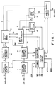
- Fig. 1 illustrates the circuit structure of an EEPROM of, for example, 64 kilobits (8192 words x 8 bits).
- a row address latch 1 latches the upper 8 bit data A12-A5 of address data A12-A0 in response to a signal d from a control circuit 10, which will be described later.
- a row address decoder 2 decodes the address data A12-A5 latched by row address latch 1 to produce a row select signal a and sends the signal a to a memory cell array 3 of 8192 words x 8 bits.
- a column address buffer 4 stores the lower 5 bit data A4-A0 of address data A12-A0.
- a column address decoder 5 decodes the address data A4-A0 from column address buffer 4 in response to a signal e (to be described later) from control circuit 10 to produce column select signals b and c .
- An access identification (ID) latch 6 latches access ID data in response to signal c from column address decoder 5
- An input data latch 7 latches 8 bit data from an input/output buffer 8, which will be described later, in response to signal c from column address decoder 5.
- the input/output buffer 8 stores 8-bit input/output data D7-D0 in response to a signal h from control circuit 10, which will be described later.
- a write controller 9 executes an internal writing operation in response to a signal f from control circuit 10, which will be described later.
- Control circuit 10 controls the data writing and reading done to the present EEPROM.
- This control circuit 10 externally receives an RST signal (signal for cancelling the internal writing operation), a WE signal (write enable signal), and an OE signal (output enable signal), and outputs a WRB signal and an RRB signal as write status signals to the outside, the latter two signals being described later.
- Fig. 2 illustrates the external writing timing for thus constituted EEPROM.
- both of the WRB and RRB signals are at an "H” level.
- the WRB signal becomes "L” level when the first byte of write bytes is accessed and again becomes “H” level when the subsequent internal writing operation is completed.
- Control circuit 10 includes a timer 11 and a counter 12.
- Timer 11 is for determining a data reception time for the next write bytes after the present write bytes have been input.
- Counter 12 counts how many times the write bytes are received.
- the data reception ends upon reception of, for example, 32 bytes.
- Timer 11 is designed to overflow upon elapse of 50 ⁇ s after being reset. In other words, the reception operation for the write bytes will end either when 50 ⁇ s has elapsed between accessing of one byte and the next byte or when accessing between bytes falls within 50 ⁇ s but 32 bytes are accessed.
- the count-up operation of counter 12 and the reset operation for timer 11 are executed by an input reception timer reset signal (pulse) that is produced by a data writing operation. It is the RRB signal which informs to the outside whether or not the data reception operation is in process, and this signal becomes "L" level upon completion of the data reception and becomes "H” level upon completion of the subsequent internal writing operation.
- both the WRB and RRB signals are "H” level, it means that the EEPROM is ready for the first byte of write bytes.
- the WRB signal is "L” level and the RRB signal is “H” level, the first byte has already been received and the reception of the subsequent bytes is being carried out.
- both of the WRB and RRB signals are "L” level, the write byte reception is inhibited and the internal writing operation is in process. This permits an external unit to easily discriminate the above three states.
- address data A12-A5 is latched as a row address in row address latch 1 by the signal (signal d in Fig. 1) resulting from a logical product of the CE and WE signals.
- the WRB signal is set to "L" level.
- column address decoder 5 decodes address data A4-A0 from column address buffer 4 based on the signal (signal e in Fig. 1) which is a logical product of the CE and WE signals, thereby producing the signal c .
- Access ID latch 6 is constituted by 32 1-bit latches and is normally reset; only that constituent latch which is selected by the signal c is set.
- Input data latch 7 is constituted by latches of 8 bits ⁇ 32 words; each 8-bit latch is selected by the signal c and the latch selected at this time latches data coming through input/output buffer 8. In other words, when data values of A4-A0 are input at random, they are stored in their associated 8-bit latches and access ID latch 6 stores data that indicates which latches the data is stored.
- the column address for the internal writing operation is set to "0" (step S31).
- This column address is generated by a column address generator (not shown) included in write controller 9 and is a value between "00" to "1F.”
- the output of the column address generator is decoded to thereby produce the row select signal i and the signals j and k .
- write controller 9 selects the associated latch in access ID latch 6, i.e., controller 9 refers to the access ID data corresponding to the column address (step S32) and discriminates whether or not the selected latch is set (step S33). If the latch is not set (or at "0"), no data writing to memory cell array 3 is performed and the address is incremented by one by the column address generator (step S34).
- write controller 9 selects the associated 8-bit latch in input data latch 7 or selects the 8-bit latch of input data latch 7 which corresponds to the column address.
- the data in the selected latch is sent to memory cell array 3, and at the same time, the memory cell to be accessed for data writing is designated by the column select signal i (column address) and row select signal a (row address) and a write permit signal l is supplied to memory cell array 3.
- memory cell array 3 Upon reception of the write permit signal l , memory cell array 3 stores data received in advance into the memory cell (of 8 bits) designated by the address data (step S35).
- Write controller 9 discriminates that the data has been written in memory cell array 3 and causes its column address generator to increment the column address by one (step S34).
- step S36 Prior to step S34 where the column address is incremented by one, however, it is determined whether or not the address is "1F H " (step S36). If the decision is affirmative, write controller 9 sends a signal m to control circuit 10 to inform that the writing operation is completed. When acknowledging the end of the writing operation through the signal m , control circuit 10 sets both the WRB and RRB signals at "H" level and resets all the latches of access ID latch 6 using a signal g , setting latch 6 back to the normal memory state.
- An read operation is performed in response to the CE and OE signals that are input during a read permit time (the period other than the internal writing period in Fig. 2). If control circuit 10 discriminates at this time that the read operation is being performed, address data A12-A5 is converted into the row select signal a by row address decoder 2 through row address latch 1. Address data A4-A0 is converted into the column select signal b by column address decoder 5 through column address buffer 4. Data in the memory cell (of 8 bits) specified by the row select signal a and column select signal b is read out and stored in input/output buffer 8 by signal h .
- control circuit 10 sets both of the WRB and RRB signals to "H” level, and, at the same time, resets all the latches of access ID latch 6, thus setting the latch 6 back to the normal memory state.
- access ID latch 6 for storing access ID data for the buffers for one page so that those buffers accessed within a specified time can be discriminated and only the contents of the buffers accessed during the internal writing operation are written in the memory cells. This can ensure that only the data received during the data reception time is accurately written in the target memory cells. Therefore, the writing times of the memory cells can be reduced, thus preventing the life of the memory cells from being shortened.
- counter 12 for counting the quantity of data received at the time of the data reception is provided so that when the quantity of the counted data reaches a predetermined value (for example, 32 bytes), the write data reception is ended and the internal writing operation is performed immediately thereafter. This reduces an overall write time loss at the time of the page writing operation, thus ensuring a higher writing operation.
- a predetermined value for example, 32 bytes
- control circuit 10 is designed to receive the internal writing cancel signal ( RST signal), which is externally generated, so that upon reception of this signal during the write data reception time, the present system resets the internal circuits to cancel the page writing operation and returns to the normal state.
- RST signal the internal writing cancel signal
- the write status signals (WRB and RRB signals) are output to the outside and the levels of these write status signals are changed at the time when the first byte is received for the page writing operation, at the time when a predetermined time has elapsed (the data reception operation is ended) and at the time when the internal writing operation is ended. This ensures an easy external detection of the data reception time for the page writing operation, thus providing an effective writing sequence as an external unit.
Landscapes
- Read Only Memory (AREA)
- Storage Device Security (AREA)
Claims (6)
- Système d'écriture de données comprenant :
un dispositif de mémoire (3) ayant des pages, chaque page comprenant une pluralité de zones de mots ;
un dispositif (7) pour recevoir et maintenir de façon externe des données appliquées à stocker dans le dispositif de mémoire (3) ; et
un dispositif de commande d'écriture (9, 10) pour écrire les données maintenues dans le dispositif de réception et de maintien (7) dans une zone de mots désignée d'une page spécifique dans le dispositif de mémoire (3) ; dans lequel
ledit dispositif de commande d'écriture (9, 10) comprend un temporisateur (11) pour compter l'intervalle de temps à partir d'un premier instant auquel une unité desdites données fournies de façon externe est reçue jusqu'à un second instant auquel l'unité suivante desdites données fournies de façon externe est reçue, et un dispositif (9, 10) pour terminer la réception des données fournies de façon externe lorsque l'unité suivante de données n'est pas reçue dans une période de temps prédéterminée comptée par le temporisateur (11), validant ainsi le transfert des données du dispositif de réception et de maintien de données (7) au dispositif de mémoire (3) immédiatement après que soit terminée la réception des données fournies de façon externe,
caractérisé en outre en ce qu'il comprend :
un dispositif de sortie (10) pour fournir à un dispositif externe des premières données (RRB) représentant si l'opération d'écriture par le dispositif de commande d'écriture (9, 10) est ou non en cours de réalisation. - Système d'écriture de données selon la revendication 1, caractérisé en ce que ledit dispositif de sortie (10) fournit en outre au dispositif externe des secondes données (WRB, RRB) représentant une période pendant laquelle les données à renouveler peuvent être reçues.
- Système d'écriture de données selon la revendication 1 ou 2, caractérisé en ce que ledit dispositif de réception et de maintien de données (7) comprend un premier dispositif de stockage (7) ayant le même nombre de mots et de bits que la page dans le dispositif de mémoire (3) pour recevoir et maintenir les données à renouveler, et un second dispositif de stockage (6) pour stocker des données d'identification représentant les emplacements de mots dans ledit premier dispositif de stockage qui sont à renouveler dans le dispositif de mémoire (3) ; et en ce que ledit dispositif de commande d'écriture (9, 10) comprend un dispositif (9, 10) pour extraire seulement les mots de données stockés dans le premier dispositif de stockage (7) qui sont désignés pour le renouvellement par ledit second dispositif de stockage afin de stocker les mots de données lus dans le dispositif de mémoire (3).
- Système d'écriture de données selon la revendication 1 ou 2, caractérisé en ce que ledit dispositif de commande d'écriture (9, 10) comprend ùn dispositif pour annuler l'opération d'écriture des données maintenues dans le dispositif de réception et de maintien de données (7) dans le dispositif de mémoire (3) en réponse à un signal externe (
RST ), lorsque le dispositif de réception et de maintien de données (7) reçoit les nouvelles données à stocker dans le dispositif de mémoire (3). - Système d'écriture de données selon la revendication 4, caractérisé en ce que ledit dispositif de commande d'écriture (9, 10) fournit à l'extérieur un signal (WRB, RRB) indiquant une période de réception de données pour ledit dispositif de réception et de maintien (7).
- Système d'écriture de données selon l'une quelconque des revendications 1 à 5, caractérisé en ce que ledit dispositif de mémoire (3) est compris dans une EEPROM.
Applications Claiming Priority (2)
| Application Number | Priority Date | Filing Date | Title |
|---|---|---|---|
| JP62104506A JPS63271679A (ja) | 1987-04-30 | 1987-04-30 | デ−タ書込み方式 |
| JP104506/87 | 1987-04-30 |
Publications (3)
| Publication Number | Publication Date |
|---|---|
| EP0288832A2 EP0288832A2 (fr) | 1988-11-02 |
| EP0288832A3 EP0288832A3 (fr) | 1991-03-20 |
| EP0288832B1 true EP0288832B1 (fr) | 1994-12-28 |
Family
ID=14382381
Family Applications (1)
| Application Number | Title | Priority Date | Filing Date |
|---|---|---|---|
| EP88105979A Expired - Lifetime EP0288832B1 (fr) | 1987-04-30 | 1988-04-14 | Système d'écriture de données pour EEPROM |
Country Status (4)
| Country | Link |
|---|---|
| US (1) | US4891791A (fr) |
| EP (1) | EP0288832B1 (fr) |
| JP (1) | JPS63271679A (fr) |
| DE (1) | DE3852562T2 (fr) |
Families Citing this family (21)
| Publication number | Priority date | Publication date | Assignee | Title |
|---|---|---|---|---|
| JPH02214994A (ja) * | 1989-02-15 | 1990-08-27 | Hitachi Maxell Ltd | Icカード |
| IL96808A (en) * | 1990-04-18 | 1996-03-31 | Rambus Inc | Introductory / Origin Circuit Agreed Using High-Performance Brokerage |
| US6751696B2 (en) | 1990-04-18 | 2004-06-15 | Rambus Inc. | Memory device having a programmable register |
| US6324120B2 (en) | 1990-04-18 | 2001-11-27 | Rambus Inc. | Memory device having a variable data output length |
| NL9000940A (nl) * | 1990-04-20 | 1991-11-18 | Nedap Nv | Universeel identificatie label. |
| KR100214435B1 (ko) * | 1990-07-25 | 1999-08-02 | 사와무라 시코 | 동기식 버스트 엑세스 메모리 |
| US5363330A (en) * | 1991-01-28 | 1994-11-08 | Mitsubishi Denki Kabushiki Kaisha | Non-volatile semiconductor memory device incorporating data latch and address counter for page mode programming |
| WO1993007565A1 (fr) * | 1991-10-01 | 1993-04-15 | Motorola, Inc. | Procede et appareil concernant la protection d'ecriture en memoire |
| US5621738A (en) * | 1991-12-10 | 1997-04-15 | Eastman Kodak Company | Method for programming flash EEPROM devices |
| ATE209819T1 (de) * | 1995-01-05 | 2001-12-15 | Macronix Int Co Ltd | Fortgeschrittene programmierverifikation für flash-speicher mit seitenmodus |
| US6810449B1 (en) | 1995-10-19 | 2004-10-26 | Rambus, Inc. | Protocol for communication with dynamic memory |
| US6470405B2 (en) * | 1995-10-19 | 2002-10-22 | Rambus Inc. | Protocol for communication with dynamic memory |
| JP3371682B2 (ja) * | 1996-04-26 | 2003-01-27 | トヨタ自動車株式会社 | 半導体記憶装置 |
| US6266379B1 (en) * | 1997-06-20 | 2001-07-24 | Massachusetts Institute Of Technology | Digital transmitter with equalization |
| WO1999019805A1 (fr) * | 1997-10-10 | 1999-04-22 | Rambus Incorporated | Procede et appareil pour operations d'ecriture dans une memoire en deux temps |
| US6401167B1 (en) * | 1997-10-10 | 2002-06-04 | Rambus Incorporated | High performance cost optimized memory |
| US6675272B2 (en) * | 2001-04-24 | 2004-01-06 | Rambus Inc. | Method and apparatus for coordinating memory operations among diversely-located memory components |
| US8391039B2 (en) * | 2001-04-24 | 2013-03-05 | Rambus Inc. | Memory module with termination component |
| US7301831B2 (en) * | 2004-09-15 | 2007-11-27 | Rambus Inc. | Memory systems with variable delays for write data signals |
| US20090307140A1 (en) * | 2008-06-06 | 2009-12-10 | Upendra Mardikar | Mobile device over-the-air (ota) registration and point-of-sale (pos) payment |
| US8862767B2 (en) | 2011-09-02 | 2014-10-14 | Ebay Inc. | Secure elements broker (SEB) for application communication channel selector optimization |
Family Cites Families (3)
| Publication number | Priority date | Publication date | Assignee | Title |
|---|---|---|---|---|
| WO1980002881A1 (fr) * | 1979-06-12 | 1980-12-24 | Motorola Inc | Micro-ordinateur avec eprom a micro-processeur programmable |
| JPS6124091A (ja) * | 1984-07-12 | 1986-02-01 | Nec Corp | メモリ回路 |
| JPS62501736A (ja) * | 1985-02-11 | 1987-07-09 | アドバンスト・マイクロ・ディバイシズ・インコ−ポレ−テッド | E↑2promsのための効率的なペ−ジモ−ド書込回路 |
-
1987
- 1987-04-30 JP JP62104506A patent/JPS63271679A/ja active Pending
-
1988
- 1988-04-14 DE DE3852562T patent/DE3852562T2/de not_active Expired - Fee Related
- 1988-04-14 EP EP88105979A patent/EP0288832B1/fr not_active Expired - Lifetime
- 1988-04-15 US US07/182,021 patent/US4891791A/en not_active Expired - Lifetime
Also Published As
| Publication number | Publication date |
|---|---|
| US4891791A (en) | 1990-01-02 |
| EP0288832A3 (fr) | 1991-03-20 |
| JPS63271679A (ja) | 1988-11-09 |
| DE3852562T2 (de) | 1995-05-04 |
| EP0288832A2 (fr) | 1988-11-02 |
| DE3852562D1 (de) | 1995-02-09 |
Similar Documents
| Publication | Publication Date | Title |
|---|---|---|
| US4891791A (en) | Data writing system for EEPROM | |
| US5930167A (en) | Multi-state non-volatile flash memory capable of being its own two state write cache | |
| KR960012359B1 (ko) | 반도체 기억장치 | |
| EP0283238B1 (fr) | Mémoire non volatile | |
| US4718041A (en) | EEPROM memory having extended life | |
| US5200600A (en) | IC card and method for writing information therein | |
| US4763305A (en) | Intelligent write in an EEPROM with data and erase check | |
| US5363334A (en) | Write protection security for memory device | |
| US5036460A (en) | Microprocessor having miswriting preventing function | |
| US5367484A (en) | Programmable high endurance block for EEPROM device | |
| US6839285B2 (en) | Page by page programmable flash memory | |
| EP0357361B1 (fr) | Carte à circuit intégré et méthode pour y inscrire des données | |
| CN101783176A (zh) | 非易失性存储装置及其操作方法 | |
| EP0806772A2 (fr) | Procédé et dispositif de protection de programmation et d'effacement d'une mémoire morte électriquement effaçable et programmable | |
| JPH0714395A (ja) | メモリカードのための集積回路とメモリカード内の単位のカウントダウン方法 | |
| US5621738A (en) | Method for programming flash EEPROM devices | |
| US6421276B1 (en) | Method and apparatus for controlling erase operations of a non-volatile memory system | |
| US4680736A (en) | Method for operating a user memory designed a non-volatile write-read memory, and arrangement for implementing the method | |
| US5285415A (en) | Data counting memory card and reader | |
| US8180976B2 (en) | Programming non-volatile memory devices based on data logic values | |
| KR100852923B1 (ko) | 반도체 메모리 | |
| JP2720013B2 (ja) | 書込みチェック機能を備えた電気的に変更可能な不揮発性メモリ | |
| US6137717A (en) | Nonvolatile memory and writing circuit for same | |
| JP2007035120A (ja) | シーケンシャルアクセスメモリ | |
| JP3378681B2 (ja) | メモリのデータ書き込み読み出し回路 |
Legal Events
| Date | Code | Title | Description |
|---|---|---|---|
| PUAI | Public reference made under article 153(3) epc to a published international application that has entered the european phase |
Free format text: ORIGINAL CODE: 0009012 |
|
| 17P | Request for examination filed |
Effective date: 19880511 |
|
| AK | Designated contracting states |
Kind code of ref document: A2 Designated state(s): DE FR |
|
| PUAL | Search report despatched |
Free format text: ORIGINAL CODE: 0009013 |
|
| AK | Designated contracting states |
Kind code of ref document: A3 Designated state(s): DE FR |
|
| 17Q | First examination report despatched |
Effective date: 19920811 |
|
| GRAA | (expected) grant |
Free format text: ORIGINAL CODE: 0009210 |
|
| AK | Designated contracting states |
Kind code of ref document: B1 Designated state(s): DE FR |
|
| REF | Corresponds to: |
Ref document number: 3852562 Country of ref document: DE Date of ref document: 19950209 |
|
| ET | Fr: translation filed | ||
| PLBE | No opposition filed within time limit |
Free format text: ORIGINAL CODE: 0009261 |
|
| STAA | Information on the status of an ep patent application or granted ep patent |
Free format text: STATUS: NO OPPOSITION FILED WITHIN TIME LIMIT |
|
| 26N | No opposition filed | ||
| PGFP | Annual fee paid to national office [announced via postgrant information from national office to epo] |
Ref country code: DE Payment date: 20060406 Year of fee payment: 19 |
|
| PGFP | Annual fee paid to national office [announced via postgrant information from national office to epo] |
Ref country code: FR Payment date: 20060410 Year of fee payment: 19 |
|
| PG25 | Lapsed in a contracting state [announced via postgrant information from national office to epo] |
Ref country code: DE Free format text: LAPSE BECAUSE OF NON-PAYMENT OF DUE FEES Effective date: 20071101 |
|
| PG25 | Lapsed in a contracting state [announced via postgrant information from national office to epo] |
Ref country code: FR Free format text: LAPSE BECAUSE OF NON-PAYMENT OF DUE FEES Effective date: 20070430 |