EP0039899A2 - Système de traitement d'un signal de balayage - Google Patents
Système de traitement d'un signal de balayage Download PDFInfo
- Publication number
- EP0039899A2 EP0039899A2 EP81103441A EP81103441A EP0039899A2 EP 0039899 A2 EP0039899 A2 EP 0039899A2 EP 81103441 A EP81103441 A EP 81103441A EP 81103441 A EP81103441 A EP 81103441A EP 0039899 A2 EP0039899 A2 EP 0039899A2
- Authority
- EP
- European Patent Office
- Prior art keywords
- signal
- analog
- voltage
- converter
- digital
- Prior art date
- Legal status (The legal status is an assumption and is not a legal conclusion. Google has not performed a legal analysis and makes no representation as to the accuracy of the status listed.)
- Granted
Links
Images




Classifications
-
- H—ELECTRICITY
- H04—ELECTRIC COMMUNICATION TECHNIQUE
- H04N—PICTORIAL COMMUNICATION, e.g. TELEVISION
- H04N1/00—Scanning, transmission or reproduction of documents or the like, e.g. facsimile transmission; Details thereof
- H04N1/40—Picture signal circuits
- H04N1/401—Compensating positionally unequal response of the pick-up or reproducing head
-
- G—PHYSICS
- G06—COMPUTING OR CALCULATING; COUNTING
- G06V—IMAGE OR VIDEO RECOGNITION OR UNDERSTANDING
- G06V10/00—Arrangements for image or video recognition or understanding
- G06V10/20—Image preprocessing
- G06V10/28—Quantising the image, e.g. histogram thresholding for discrimination between background and foreground patterns
-
- H—ELECTRICITY
- H04—ELECTRIC COMMUNICATION TECHNIQUE
- H04N—PICTORIAL COMMUNICATION, e.g. TELEVISION
- H04N1/00—Scanning, transmission or reproduction of documents or the like, e.g. facsimile transmission; Details thereof
- H04N1/40—Picture signal circuits
- H04N1/403—Discrimination between the two tones in the picture signal of a two-tone original
Definitions
- the present invention relates to a scanning signal processing system, and more particularly to an analog scanning signal processing system for converting an analog scanning signal having a substantially constant shading profile to a multi-level signal.
- an analog signal When an analog signal is converted to a multi-level of multi-state signal such as bi-level or tri- level signal, the analog signal voltage is compared with a reference voltage or reference voltages to produce the multi-level signal.
- the conversion precision depends on the precisions of the analog voltage and the reference voltage.
- optical information such as characters on a document sheet is scanned by photo-electric converter means to produce an analog video signal, which is then converted to a multi-level video signal.
- the analog video signal may be produced by superimposing the information signal on a background representing a plain paper.
- the conversion precision depends on a distribution of illumination on the document sheet and image forming conditions of an optical system including lenses.
- the conversion precision further depends on a distribution of sensitivity,of sensor elements of the line sensor.
- the document sheet is plane ( e .g.
- the scanned analog video signal (referred to as a white scan signal train) may not have a constant voltage level but have a specific profile. This profile is reproduced in each scan with a substantially same pattern.
- a characteristic distribution of the analog video scan signal representing background (state of no information) is called shading.
- a general or relative characteristic distribution is called a shading profile, and a characateristic distribution including voltage level is called a shading characteristic, in this specification.
- the illumination of the document sheet may be adjusted by rearranging a light source or disposing a filter or a mask so that a white scan signal train having a constant signal level is produced.
- This method needs a complex and large device and takes long time for adjustment and is hard to attain a sufficient effect.
- the electrical compensation includes a way of controlling a gain of a video amplifier to produce a shading-free video signal and another way of effecting compensation in a signal processing step of converting an analog signal containing shading to a multi-level signal.
- Japanese Patent Appliation No. 52-9761 (Laid-Open No. 53-95518) teaches to compensate a video signal produced by scan by dividing the video signal by a shading signal read out of a memory.
- the analog video signal is usually converted to a bi-level (digital) signal.
- a slice signal which varies in accordance with the shading may be used.
- Japanese Patent Application No. 48-130508 (Laid-Open No. 50-81419) teaches to compensate a slice signal for discriminating a video signal by a shading signal read out of a read-only memory (ROM).
- ROM read-only memory
- a high speed, large capacity memory and high speed processing circuit components can store and reproduce any level and any form of shading but they are not desirable from a standpoint of stability and economy.
- shading compensation with a high precision is attained with a given capacity of memory.
- the shading profile can be stored in the given capacity of memory with a high precision.
- the normalized shading profile is denormalized basically by a current peak voltage of the scan signal trains so that an instantaneous shading characteristic including the voltage level can be reproduced with a high precision regardless of a variation in the background of a text.
- the reproduction of a rising edge of the shading profile may need a high speed operation of the signal processing circuit components.
- the rising edge of the shading characteristic can be reproduced with a high fidelity with relatively low speed components. This is particularly effective when an external memory is used with a serial access mode.
- a documnt 10 driven in a direction of an arrow by drivemeans (not shown) is illuminated by a lamp 11 and a scanning line area extending widthwise of the document (normal to the direction of drive) is imaged on a photo-sensitive plane of a photo-electric converter array 13 through a lens 12.
- the photo-electric converter array 13 may be a CCD line sensor which may comprise 2048 picture cells. Voltage signals produced in the respective picture cells of the photo-electric array 13 are taken out serially in the order of cell arrangement and applied to an analog video input terminal 1 as an analog video signal A.
- Such an analog video signal A usually includes 20 - 40 % shading.
- Numeral 2 denotes a peak hold circuit which holds a peak value of the analog video signal A applied to the video input terminal 1 and produces an analog peak voltage B.
- An analog-to-digital converter 3 in a converter circuit 14 receives the analog video signal A for the scan of a white area (top of the document sheet) and the analog peak voltage B, and produces a digital coded shading profile signal C which is normalized by the analog peak voltage B and supplies the signal C to a memory 4, which stores the normalized shading profile signal C.
- the normalization is carried out by scaling the voltage of the analog video signal A using the peak voltage B as a reference. Any unit and any scale may be selected.
- the peak hold circuit 2 produces an instantaneous peak voltag Vp which follows a change in the background of the document sheet.
- a digital-to-analog converter 5 in the converter circuit 14 receives the normalized shading profile signal C which is read out of the memory and a current analog peak voltage B produced by the peak hold circuit 2 and produces an analog reference voltage D corresponding to white or plain background at that time. By appropriately dividing the analog reference voltage D, a shading-compensated slice signal D' is produced.
- Numeral 6 denotes a discrimination circuit which compares the analog video signal A carrying the image information with the slice signal D' derived by dividing the reference voltage D to produce a multi-level information signal E at an output terminal 7.
- the operations of the photo-electric converter array 13, the memory 4 and the converter 14 including the analog-to-digital converter 3 and the digital-to-analog converter 5 are controlled by timing signals from a control circuit 88.
- the circuit elements in a broken line 1 may be integrated in one chip LSI.
- the analog information signal A which is produced by repetitively and photo-electrically scanning the document sheet includes white scan signal trains A-1 and A-2 and and information scan signal trains A-3, ...
- the white scan signal train A-1 is applied to the peak hold circuit 2 which holds a peak value thereof and produces a peak hold voltage B at the output.
- the next incoming white scan signal train A-2 is normalized by the peak hold voltage B for each picture cell and digitized to produce a shading profile signal C for all picture elements of a scanning line.
- the normalized digitization may be carried out by digitizing the white scan signal train A-2 for all the picture elements while putting the peak hold voltage to a most significant digit MSB (a maximum value in digital representation) and a zero volt signal to a least significant digit LSB (a minimum value in digital representation).
- the digi- tazation may be carried out by dividing the white scan signal train A-2 by time axis and sampling the divided signals independently, or by sequentially comparing the current picture cell value with the previous picture cell value.
- the digital signals C are sequentially stored in corresponding addresses of the memory 4. In this manner, the normalized digitization and the storage (storage of the shading profile) of the white scan signal train (e.g. plain background of the document sheet) are completed.
- the signal processing system proceeds to the process of converting the analog scan signal train to a multi-level signal. This shift of operation takes place in response to the detection of a predetermined time after the initiation of the photo-electric conversion of the document sheet or to that of a predetermined number of scannign lines.
- the analog scan signal train A-3 carrying the image information is applied to the information input terminal 1.
- the shading profile digital signals stored at the addresses corresponding to the picture cell positions in the memory 4 are read out and applied to the digital-to-analog converter 5.
- the digital-to-analog converter 5 also receives the peak-hold voltage B and produces the reference voltage D having the possible maximum value at the peak-hold voltage B.
- the peak hold circuit 2 By constructing the peak hold circuit 2 such that it always holds a peak value of the current analog scan signal train A, it is possible to produce the reference voltage D adapted to the analog scan signal train A-3 even when the plain background of the document sheet varies.
- the reference voltage D thus produced is applied to the discrimination circuit 6 which produces a slice voltage D', which in turn is compared with the analog scan signal train A-3 to produce a bi-level information signal E.
- a plurality of slice voltages are used to produce a multi-level signal, gray information can be reproduced. By changing the slice voltage, a black-white discrimination level can be varied.
- Fig. 3 and 4 show examples of the peak hold circuit 2.
- Fig. 3 shows an analog processing circuit-and
- Fig. 4 shows a digital processing circuit.
- numeral 21 denotes an operational amplifier
- numeral 22 denotes a voltage follower
- numeral 23 denotes a diode
- numeral 24 denotes a voltage holding capacitor
- numeral 29 denotes a resistor determining the discharge time constant.
- the analog scan signal train A is supplied to the capacitor 24 through the operational amplifier 21 and the diode 23 and a peak value thereof is held in the capacitor 24.
- the charge stored in the capacitor 24 is gradually discharged through the resistor 29 to follow the current peak value of the analog scan signal train.
- the peak value is applied to the voltage follower 22 which produces the peak hold voltage B.
- the resistor 29 may be disconnected.
- the resistor 29 may be substituted by a potentiometer to adjust the time constant or it may be substituted by a controlled switch to allow resetting of the peak hold voltage B.
- numeraal 25 denotes a comparator
- numeral 26 denotes an address counter
- numeral 27 denotes a digital-to-analog converter.
- the comparator 25 receives the analog scan signal train A from the information input terminal 1 and compares it with an output of the digital-to-analog converter 27 (peak hold voltage B).
- the analog scan signal train A When the analog scan signal train A is larger than the peak hold voltage B, it produces a control output which renders the address counter 26 to count up clock pulses CP.
- the count in the address counter 26 is converted to an analog signal by the digital-to-analog converter 27, which analog signal constitutes the voltage B.
- the volage B provides a peak value of the applied analog scan signal train A.
- an up/down counter may be used as the address counter 26 and the count thereof may be periodically decremented, as taught in Japanese Patent Application No. 55-60571 filed on May 9, 1980.
- the peak hold operation for the analog scan signal train A described above starts immediately after the initiation of the photo-electric scan of the document sheet and is cleared when the scan has been completed.
- the digital-to-analog converter 27 may be constructed in a similar manner as the digital-to-analog converter 5 which will be explained later.
- Fig. 5 shows an example of the analog-to-digital converter 3 used to store the shading profile.
- Numeral 31 denotes a voltage dividing resistor which is connected to the output terminal of the peak hold circuit 2 described above.
- Numeral 32 denotes semiconductor gate switches which are connected between voltage dividing terminals of the voltage dividing resistor 31 and a reference input terminal of a comparator 33. The gate switches 32 are controlled by outputs of a decoder 34 and a voltage determined by the selected switch is supplied to the reference voltage termainl of the comparator 33.
- the comparator 33 compares the analog scan- signal train A with the output voltage from the gate switches 32 to produce a difference signal, which is then fed back to a counter 36 through an up/down control circuit 35 so that the inputs to the comparator 33 are made equal. More particularly, when the analog scan signal train A is larger than the output voltage of the gate switches 32, the counter 36 counts up the clock signals, and when the former is smaller than the latter, the counter 36 counts down the clock signals. The output from the counter 36 provides the digital signal C which corresponds to the shading profile normalized by the peak hold voltage B. The digital signal C is stored in the memory 4 at addresses corresponding to the picture cell position.
- Fig. 6 shows an example of the digital-to-analog converter 5.
- Numeral 51 denotes a voltage dividing resistor which is connected to the output terminal of the peak hold circuit 2 described above.
- Numeral 52 denotes semiconductor gate switches which are connected between voltage dividing terminals of the voltage dividing resistor 51 and the discriminator circuit 6.
- a decoder 54 receives the digital signal C read out of the memory 4 and controls the gate switches 52.
- Fig. 7 shows an example of the discriminator circuit 6.
- Numeral 61 denotes a voltage dividing resistor which is connected to the output terminal of the digital-to-analog converter 5 and to which the reference voltage D is applied.
- Numeral 62 denotes comparators which receive respective slice voltages from respective voltage dividing terminals of the voltage dividing resistor. Each comparator 62 compares the analog scan signal train A with the slice voltage to produce bi-level signal.
- Numeral 63 denotes a selection switch which selects any one of the outputs from the comparators 62 and supplies the selected output to the output terminal 7 as the bi-level information signal E.
- the precision in converting the analog scan signal train to the multi-level signal train depends on the precision of the peak hold circuit to reproduce the peak value, and the precision of conversion in the analog-to-digital converter 3 and the digital-to-analog converter 5 of the converter circuit 14.
- the entire conversion precision depends on the conversion precisions of the analog-to- ditigal converter and the digital-to-analog converter.
- each converter may handles 7-bit (128-step) digital signals and coresponding analog voltages. Those analog voltage steps are preferably distributed effectively in a voltage range of the voltage signals to be handled from a standpoint of precision.
- the voltage dividing resistors 31 and 51 of the converters 3 and 5 must be divided at the same step in order to allow the reproduction of the signal with high fidelity.
- the voltage division in the converter 27 may differ from the voltage divisions in the converters 3 and 5.
- the voltage range is preferably divided by a geometric progression (exponentially) in order to assure a uniformly high precision irrespective of the magnitude of the voltage signal.
- V n iY n and Y n Y n-1 /(1- ⁇ o ).
- the error ⁇ is constant. Since the voltage dividing terminals are not required in the voltage range which is not used, the resistances y , and y may be determined in accordance with the minimum and the maximum of the voltage range used.
- the parallel signal transfer causes a pin-neck.
- the output of the comparator 33 may be supplied as a serial signal as will be explained later.
- the output from the memory may be supplied as a serial signal and applied to the decoder through a serial-parallel converter.
- the parallel signal transfer does not raise a problem and the input and output of the memory may be parallel signals as shown.
- the illustrated embodiment uses the resistor strings having the voltage dividing terminals, other voltage dividing resistor networks such as resistor matrix or resistor tree may be used.
- While the illustrated embodiment uses the line sensor to effect the photo-electric scan, a single sensor and deflection mirror may be used or a matrix sensor may be used to effect the photo-electric conversion of a plurality of scan lines simultaneously.
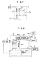
- Fig. 8 shows a block diagram of another embodiment in which components of the analog-to-digital converter and the digital-to-analog converter are partially shared.
- the information input terminal 1 and the peak hold circuit 2 are similar to those shown in the previous embodiment.
- Numeral 83 denotes a signal converter circuit which has the functions of the analog-to-digital converter 3 and the digital-to-analog converter 5 of the previous embodiment but the construction is substantially similar as the analog-to-digital converter shown in Fig. 5.
- Numeral 831 denotes a voltage dividing resistor
- 832 denotes semiconductor gate switches
- 834 denotes a decoder
- 835 denotes an up/down control circuit
- 836 denotes a counter.
- Numeral 6 denotes a discriminator circuit which is similar to that shown in Fig. 7.
- the input circuit of the discriminator 6 is connected in common to the through a buffer circuit 85 and a bi-level information signal E is produced at the output terminal 7.
- Numeral 4 denotes the memory an input/output circuit of which is connected to an output terminal of the counter 836.
- Numeral 88 denotes a control circuit which supplies timing pulses to the up/down controller 835 and the memory 4 so that the signal converter circuit 83 selectively operates as the analog-to-digital converter or the digital-to-analog converter.
- the signal converter circuit 83 is controlled by the control circuit 88 such that it operates as the analog-to-digital converter to store the shading profile.
- the up/down controller 835 supplies an increment or decrement signal to the counter 836 depending on the output from the comparator 833, and the memory 4 assumes a write state.
- the peak hold circuit 2 holds a peak value of the white scan signal train A-1 and compares the subsequently supplied white scan signal train A-2 with the peak hold voltage B to produce the normalized shading profile digital signal C, which is then stored in the memory 4.
- the storage operation is identical to that carried out in the analog-to-digital converter shown in Fig. 5.
- the control circuit 88 renders the up/down controller 835 to assume a rest state and renders the memory 4 to assume a read state.
- the digital signal C is read out of the memory 4 from the address corresponding to the picture cell position of the scan signal train A-3 applied to the analog information input terminal 1.
- the semiconductor gate switches 832 are controlled to produce the reference voltage denormalized by the peak hold voltage B. This operation is similar to that of the digital-to-analog converter shown in Fig. 6.
- the analog scan signal train A-3 and the reference voltage D are applied to the discriminator circuit 6 which produces the bi-level information signal E.
- the operation of the discriminator circuit 6 is identical to that shown in Fig. 7.
- Fig. 9 shows an embodiment in which the input and the output of the memory are serial signals and a high precision signal processing is attained with relatively low speed circuit components;
- the like numerals as in the previous figures denote the like elements.
- An up/down counter 936 includes an up/down controller and it counts up or down clock pulses CLK1 under the control of the output of the comparator 833.
- a load signal LD When a load signal LD is applied thereto, it loads a parallel output of a serial-parallel (S/P) converter 937.
- the parallel output of the up/down counter 936 is converted to a serial signal by a parallel-serial (P/S) converter 938 and the serial signal is stored in a memory 4'.
- the serial output of the memory 4' is either supplied directly to the up/down counter 936 or converted to a parallel signal by the serial-parallel converter 937 and then the parallel signal is supplied to the up/down counter 936.
- FIG. 10 An initial value Vi of an analog video signal train A shown in Fig. 10 is detected and stored.
- the clock signals CLK1 are counted up by the up/down counter 936 throughout each initial period of the analog video signal train A which is repetitively applied.
- the output voltage D of the semiconductor gate switch 832 selected by the decoder 834, or the output of the converter 93 rises.
- the count-up operation of the up/down counter 936 is controlled by the output of the comparator 833 and it continues until the initial value Vi is reached by the output voltage D of the gate 832, when the count-up operation is stopped.
- the count in the up/down counter 936 represents the digital value of the initial value Vi normalized by the peak voltage held in the peak hold circuit 2.
- this value is stored in the memory 4' as a serial signal.
- the clock signals CLK1 are controlled to be supplied continuously during each scan period.
- the incoming analog video signal train A is compared with the output voltage D of the gate 832 by the comparator 833, which produces an output to control the up or down mode of the up/down counter 936. In this manner, the output voltage D of the gate 832 follows the waveform of the analog video signal train A.
- the serial output signal of the comparator 833 which represents the change in the content of the up/down counter 936 is stored as the variation of the shading profile relative to the preceding value.
- the initial value of the shading profile and the subsequent changes thereof are separately stored in the memory 4' through separate paths.
- the storage operation of the shading profile has thus been explained. For example, for a line sensor of 2048 bits, the shading profile therefrom can be stored in a memory of 2048 or 1024 bits.
- the reproduction of the slice signal is now explained.
- the normalized digital value of the initial value Vi stored in the memory 4' is read out to the serial-parallel converter 937 by supplying a clock CLK2 to the serial-parallel converter 937.
- the load signal LD is supplied to the up/down counter 936 to load the parallel output of the serial-parallel converter 937 (normalized digital value of the initial value Vi) to the counter 936.
- the decoder 834 selects one of the gate switches 832 so that the initial value of the shading characteristic which is denormalized by the current peak voltage is produced at the output of the gate 832.
- drive clocks CLK1 are supplied to the up/down counter 936 and the changes of the shading profile stored in the memory 4' is read out to control the up and down modes of the up/down counter 936.
- the gate 832 or the digital-to-analog converter 93 produces the reference voltage D which approximates the shading characteristic of the instantaneous scan line.
- the output voltage D is appropriately divided in the discriminator circuit 6 to produce the slice signal D'.
- the reproduced waveform does not represent a correct shading characteristic during a time period to during which the output voltage D of the digital-to-analog converter 93 rises, as shown in Fig. 11.
- the digital signal comprises seven bits (128 steps) and the output voltage D rises step by step at a lMHz clock, a time period of 128 microseconds is needed for the output voltage D to rise to the peak value.
- one scan line comprises 2048 bits, the output voltage D cannot correctly reproduce the shading characteristic for the heading portion of 128/2048 of each scan line.
- the period t 0 is short enough to be neglected if the high speed signal processing system is used although the high speed signal processing system is expensive.
- the initial value Vi is loaded parallelly to the up/down counter 71 upon the reception of the analog video signal train A, the output voltage D of the digital-to-analog converter 93 immediately follows the shading characteristic so that the correctness of the slice signal is enhanced.
Landscapes
- Engineering & Computer Science (AREA)
- Multimedia (AREA)
- Signal Processing (AREA)
- Physics & Mathematics (AREA)
- General Physics & Mathematics (AREA)
- Theoretical Computer Science (AREA)
- Facsimile Image Signal Circuits (AREA)
Applications Claiming Priority (4)
| Application Number | Priority Date | Filing Date | Title |
|---|---|---|---|
| JP60566/80 | 1980-05-09 | ||
| JP60565/80 | 1980-05-09 | ||
| JP6056580A JPS56157575A (en) | 1980-05-09 | 1980-05-09 | Signal procession device |
| JP6056680A JPS56157576A (en) | 1980-05-09 | 1980-05-09 | Signal procession device |
Publications (3)
| Publication Number | Publication Date |
|---|---|
| EP0039899A2 true EP0039899A2 (fr) | 1981-11-18 |
| EP0039899A3 EP0039899A3 (en) | 1983-01-05 |
| EP0039899B1 EP0039899B1 (fr) | 1985-02-13 |
Family
ID=26401637
Family Applications (1)
| Application Number | Title | Priority Date | Filing Date |
|---|---|---|---|
| EP81103441A Expired EP0039899B1 (fr) | 1980-05-09 | 1981-05-06 | Système de traitement d'un signal de balayage |
Country Status (3)
| Country | Link |
|---|---|
| US (1) | US4420742A (fr) |
| EP (1) | EP0039899B1 (fr) |
| DE (1) | DE3168865D1 (fr) |
Cited By (7)
| Publication number | Priority date | Publication date | Assignee | Title |
|---|---|---|---|---|
| WO1983002185A1 (fr) * | 1981-12-17 | 1983-06-23 | Ncr Co | Procede et systeme de synchronisation pendant la reconnaissance de caracteres |
| EP0181321A3 (fr) * | 1984-11-08 | 1987-06-10 | MUPID COMPUTER GESELLSCHAFT m.b.H. | Procédé et dispositif pour la transmission du signal d'un point d'image |
| EP0158409A3 (fr) * | 1984-04-05 | 1988-03-23 | The British Library Board | Détecteur de seuil perfectionné |
| EP0257747A3 (fr) * | 1986-07-15 | 1990-01-17 | OIS Optical Imaging Systems, Inc. | Réseau photo-électrique pour balayer de grandes surfaces non-planes portant des images |
| US5267055A (en) * | 1988-05-11 | 1993-11-30 | Canon Kabushiki Kaisha | Image signal processing apparatus |
| DE19714945A1 (de) * | 1996-04-10 | 1997-11-06 | Samsung Electronics Co Ltd | Ein eine Abbildung bildendes Gerät für eine Halbton-Aufzeichnungs- und -Schattierungs-Kompensation und ein eine Halbton-Abbildung bildendes Verfahren |
| EP0539022B1 (fr) * | 1991-09-20 | 1998-04-15 | Toa Medical Electronics Co., Ltd. | Analyseur de particules |
Families Citing this family (23)
| Publication number | Priority date | Publication date | Assignee | Title |
|---|---|---|---|---|
| JPS57160221A (en) * | 1981-03-28 | 1982-10-02 | Olympus Optical Co Ltd | Analog to digital conversion system |
| US4538915A (en) * | 1981-12-23 | 1985-09-03 | E. I. Du Pont De Nemours And Company | Web inspection system having a product characteristic signal normalizing network |
| JPS58172061A (ja) * | 1982-04-02 | 1983-10-08 | Nippon Telegr & Teleph Corp <Ntt> | 信号処理装置 |
| DE3413651C3 (de) * | 1983-04-12 | 1997-11-20 | Canon Kk | Bildsignalverarbeitungsgerät |
| US4586026A (en) * | 1983-11-07 | 1986-04-29 | Liston Edwards, Inc. | Infrared gas analyzer using count quadrature sampling |
| JPS60182870A (ja) * | 1984-03-01 | 1985-09-18 | Canon Inc | 画像処理装置 |
| JPH0666885B2 (ja) * | 1985-02-15 | 1994-08-24 | キヤノン株式会社 | 画像読取装置 |
| JPS6260074A (ja) * | 1985-09-10 | 1987-03-16 | Tokyo Electric Co Ltd | バ−コ−ドスキヤナ− |
| US5115478A (en) * | 1986-01-10 | 1992-05-19 | Minolta Camera Kabushiki Kaisha | Image reader |
| US4870501A (en) * | 1986-04-24 | 1989-09-26 | Canon Kabushiki Kaisha | Image readout apparatus |
| JPS6416067A (en) * | 1987-07-08 | 1989-01-19 | Minolta Camera Kk | Original detector |
| JPS6469159A (en) * | 1987-09-10 | 1989-03-15 | Minolta Camera Kk | Picture reader |
| JPS6469157A (en) * | 1987-09-10 | 1989-03-15 | Minolta Camera Kk | Picture reader |
| US5208873A (en) * | 1987-09-10 | 1993-05-04 | Minolta Camera Kabushiki Kaisha | Image reader having an editor for setting a threshold value |
| US5027117A (en) * | 1988-03-31 | 1991-06-25 | Ricoh Company, Ltd. | Conversion using a variable reference based on image density |
| US5079698A (en) * | 1989-05-03 | 1992-01-07 | Advanced Light Imaging Technologies Ltd. | Transillumination method apparatus for the diagnosis of breast tumors and other breast lesions by normalization of an electronic image of the breast |
| US5077806A (en) * | 1989-06-01 | 1991-12-31 | Accuron Corporation | Machine vision analysis apparatus |
| US5073857A (en) * | 1989-06-01 | 1991-12-17 | Accuron Corporation | Method and apparatus for cell analysis |
| US5341217A (en) * | 1990-03-06 | 1994-08-23 | Martin Marietta Corporation | Digital adaptive video synchronizer |
| JPH07283944A (ja) * | 1994-04-07 | 1995-10-27 | Fujitsu Ltd | 画像読み取り装置における白レベル情報補正装置及び白レベル情報補正装置付き画像読み取り装置 |
| US20030042399A1 (en) * | 2001-06-19 | 2003-03-06 | Umax Data Systems Inc. | Calibration method of an image-capture apparatus |
| WO2003067269A2 (fr) * | 2002-02-05 | 2003-08-14 | Allegro Microsystems, Inc. | Detecteur de signal crete a crete |
| KR20100041428A (ko) * | 2008-10-14 | 2010-04-22 | 삼성전자주식회사 | 화상독취장치 및 쉐이딩 보정 방법 |
Family Cites Families (5)
| Publication number | Priority date | Publication date | Assignee | Title |
|---|---|---|---|---|
| US3599151A (en) * | 1969-12-29 | 1971-08-10 | Ibm | Character recognition photosensing apparatus having a threshold comparator circuit |
| US3872434A (en) * | 1973-12-05 | 1975-03-18 | Recognition Equipment Inc | Dynamic sample-by-sample automatic gain control |
| JPS5437626A (en) * | 1977-08-30 | 1979-03-20 | Sharp Corp | Correction system for facsimile read output |
| US4128830A (en) * | 1977-09-26 | 1978-12-05 | International Business Machines Corporation | Apparatus for providing a compensation signal for individual light sensors arranged in a predetermined relation |
| GB2098774B (en) * | 1979-07-20 | 1984-02-01 | Sumitomo Electric Industries | Binary coding circuit |
-
1981
- 1981-05-04 US US06/260,090 patent/US4420742A/en not_active Expired - Lifetime
- 1981-05-06 EP EP81103441A patent/EP0039899B1/fr not_active Expired
- 1981-05-06 DE DE8181103441T patent/DE3168865D1/de not_active Expired
Cited By (10)
| Publication number | Priority date | Publication date | Assignee | Title |
|---|---|---|---|---|
| WO1983002185A1 (fr) * | 1981-12-17 | 1983-06-23 | Ncr Co | Procede et systeme de synchronisation pendant la reconnaissance de caracteres |
| EP0158409A3 (fr) * | 1984-04-05 | 1988-03-23 | The British Library Board | Détecteur de seuil perfectionné |
| EP0181321A3 (fr) * | 1984-11-08 | 1987-06-10 | MUPID COMPUTER GESELLSCHAFT m.b.H. | Procédé et dispositif pour la transmission du signal d'un point d'image |
| AT388819B (de) * | 1984-11-08 | 1989-09-11 | Mupid Computer Gmbh | Anordnung zur uebertragung des signals eines bildpunktes |
| EP0257747A3 (fr) * | 1986-07-15 | 1990-01-17 | OIS Optical Imaging Systems, Inc. | Réseau photo-électrique pour balayer de grandes surfaces non-planes portant des images |
| US5267055A (en) * | 1988-05-11 | 1993-11-30 | Canon Kabushiki Kaisha | Image signal processing apparatus |
| EP0539022B1 (fr) * | 1991-09-20 | 1998-04-15 | Toa Medical Electronics Co., Ltd. | Analyseur de particules |
| DE19714945A1 (de) * | 1996-04-10 | 1997-11-06 | Samsung Electronics Co Ltd | Ein eine Abbildung bildendes Gerät für eine Halbton-Aufzeichnungs- und -Schattierungs-Kompensation und ein eine Halbton-Abbildung bildendes Verfahren |
| DE19714945C2 (de) * | 1996-04-10 | 1998-12-24 | Samsung Electronics Co Ltd | Verfahren zur Erzeugung eines Halbtonbildes und Abtastvorrichtung |
| CN1096175C (zh) * | 1996-04-10 | 2002-12-11 | 三星电子株式会社 | 网点影印及色泽补偿影印机和网点影印法 |
Also Published As
| Publication number | Publication date |
|---|---|
| EP0039899A3 (en) | 1983-01-05 |
| US4420742A (en) | 1983-12-13 |
| EP0039899B1 (fr) | 1985-02-13 |
| DE3168865D1 (en) | 1985-03-28 |
Similar Documents
| Publication | Publication Date | Title |
|---|---|---|
| US4420742A (en) | Scan signal processing system | |
| US4554583A (en) | Shading correction device | |
| US4686579A (en) | Image processing apparatus | |
| US4578711A (en) | Video data signal digitization and correction system | |
| US4594733A (en) | Signal processing system and the method | |
| US5479207A (en) | System and method for improving the signal to noise ratio of a CCD sensor in an optical scanner | |
| US4402087A (en) | Binary coding circuit | |
| US4367457A (en) | Signal processing apparatus | |
| US4571573A (en) | Apparatus for converting an analog signal to a binary signal | |
| JPS60182870A (ja) | 画像処理装置 | |
| JP3091084B2 (ja) | 信号処理回路 | |
| US4812667A (en) | Past record correcting/reading apparatus | |
| US4763201A (en) | Image readout apparatus | |
| JPS6339141B2 (fr) | ||
| US5093733A (en) | Image signal processing device | |
| JP2915448B2 (ja) | イメージセンサの2値化出力方法 | |
| JP2614738B2 (ja) | 画像入力装置 | |
| KR0157361B1 (ko) | 화신호 처리장치 | |
| JP2506643B2 (ja) | 前歴補正読取装置 | |
| JP2618655B2 (ja) | 画像読み取り装置 | |
| JPH01190078A (ja) | 画像読取り装置の基準白レベル設定方法 | |
| JPS6172474A (ja) | シエ−デイング補正方式 | |
| JPS6172472A (ja) | シエ−デイング補正方式 | |
| JPH04347972A (ja) | 密着型イメージセンサ | |
| JPH01865A (ja) | 画信号補正回路 |
Legal Events
| Date | Code | Title | Description |
|---|---|---|---|
| PUAI | Public reference made under article 153(3) epc to a published international application that has entered the european phase |
Free format text: ORIGINAL CODE: 0009012 |
|
| AK | Designated contracting states |
Designated state(s): DE FR GB NL |
|
| PUAL | Search report despatched |
Free format text: ORIGINAL CODE: 0009013 |
|
| AK | Designated contracting states |
Designated state(s): DE FR GB NL |
|
| 17P | Request for examination filed |
Effective date: 19830208 |
|
| GRAA | (expected) grant |
Free format text: ORIGINAL CODE: 0009210 |
|
| AK | Designated contracting states |
Designated state(s): DE FR GB NL |
|
| RIN1 | Information on inventor provided before grant (corrected) |
Inventor name: NAKANO, TAIZOH Inventor name: TANNO, KIYOHIKO Inventor name: TADAUCHI, MASAHARU |
|
| REF | Corresponds to: |
Ref document number: 3168865 Country of ref document: DE Date of ref document: 19850328 |
|
| ET | Fr: translation filed | ||
| REG | Reference to a national code |
Ref country code: GB Ref legal event code: 732 |
|
| PLBE | No opposition filed within time limit |
Free format text: ORIGINAL CODE: 0009261 |
|
| STAA | Information on the status of an ep patent application or granted ep patent |
Free format text: STATUS: NO OPPOSITION FILED WITHIN TIME LIMIT |
|
| 26N | No opposition filed | ||
| REG | Reference to a national code |
Ref country code: FR Ref legal event code: TP |
|
| NLS | Nl: assignments of ep-patents |
Owner name: HITACHI LTD. EN NIPPON TELEGRAPH AND TELEPHONE COR |
|
| PGFP | Annual fee paid to national office [announced via postgrant information from national office to epo] |
Ref country code: FR Payment date: 20000425 Year of fee payment: 20 |
|
| PGFP | Annual fee paid to national office [announced via postgrant information from national office to epo] |
Ref country code: GB Payment date: 20000502 Year of fee payment: 20 |
|
| PGFP | Annual fee paid to national office [announced via postgrant information from national office to epo] |
Ref country code: NL Payment date: 20000531 Year of fee payment: 20 |
|
| PGFP | Annual fee paid to national office [announced via postgrant information from national office to epo] |
Ref country code: DE Payment date: 20000630 Year of fee payment: 20 |
|
| PG25 | Lapsed in a contracting state [announced via postgrant information from national office to epo] |
Ref country code: GB Free format text: LAPSE BECAUSE OF EXPIRATION OF PROTECTION Effective date: 20010505 |
|
| PG25 | Lapsed in a contracting state [announced via postgrant information from national office to epo] |
Ref country code: NL Free format text: LAPSE BECAUSE OF EXPIRATION OF PROTECTION Effective date: 20010506 |
|
| REG | Reference to a national code |
Ref country code: GB Ref legal event code: PE20 Effective date: 20010505 |
|
| NLV7 | Nl: ceased due to reaching the maximum lifetime of a patent |
Effective date: 20010506 |