EP0040043B1 - Résistance dépendant de la tension - Google Patents
Résistance dépendant de la tension Download PDFInfo
- Publication number
- EP0040043B1 EP0040043B1 EP81301998A EP81301998A EP0040043B1 EP 0040043 B1 EP0040043 B1 EP 0040043B1 EP 81301998 A EP81301998 A EP 81301998A EP 81301998 A EP81301998 A EP 81301998A EP 0040043 B1 EP0040043 B1 EP 0040043B1
- Authority
- EP
- European Patent Office
- Prior art keywords
- voltage
- zinc oxide
- oxide layer
- oxide
- dependent resistor
- Prior art date
- Legal status (The legal status is an assumption and is not a legal conclusion. Google has not performed a legal analysis and makes no representation as to the accuracy of the status listed.)
- Expired
Links
- 230000001419 dependent effect Effects 0.000 title claims description 32
- XLOMVQKBTHCTTD-UHFFFAOYSA-N Zinc monoxide Chemical compound [Zn]=O XLOMVQKBTHCTTD-UHFFFAOYSA-N 0.000 claims description 108
- 239000011787 zinc oxide Substances 0.000 claims description 54
- 229910044991 metal oxide Inorganic materials 0.000 claims description 24
- 150000004706 metal oxides Chemical class 0.000 claims description 24
- AMWRITDGCCNYAT-UHFFFAOYSA-L hydroxy(oxo)manganese;manganese Chemical compound [Mn].O[Mn]=O.O[Mn]=O AMWRITDGCCNYAT-UHFFFAOYSA-L 0.000 claims description 12
- QVQLCTNNEUAWMS-UHFFFAOYSA-N barium oxide Chemical compound [Ba]=O QVQLCTNNEUAWMS-UHFFFAOYSA-N 0.000 claims description 6
- 239000000470 constituent Substances 0.000 claims description 6
- YEXPOXQUZXUXJW-UHFFFAOYSA-N oxolead Chemical compound [Pb]=O YEXPOXQUZXUXJW-UHFFFAOYSA-N 0.000 claims description 6
- UFQXGXDIJMBKTC-UHFFFAOYSA-N oxostrontium Chemical compound [Sr]=O UFQXGXDIJMBKTC-UHFFFAOYSA-N 0.000 claims description 6
- 229910001404 rare earth metal oxide Inorganic materials 0.000 claims description 6
- 229910000428 cobalt oxide Inorganic materials 0.000 claims description 5
- IVMYJDGYRUAWML-UHFFFAOYSA-N cobalt(ii) oxide Chemical compound [Co]=O IVMYJDGYRUAWML-UHFFFAOYSA-N 0.000 claims description 5
- AJNVQOSZGJRYEI-UHFFFAOYSA-N digallium;oxygen(2-) Chemical compound [O-2].[O-2].[O-2].[Ga+3].[Ga+3] AJNVQOSZGJRYEI-UHFFFAOYSA-N 0.000 claims description 5
- 229910001195 gallium oxide Inorganic materials 0.000 claims description 5
- PNEYBMLMFCGWSK-UHFFFAOYSA-N Alumina Chemical compound [O-2].[O-2].[O-2].[Al+3].[Al+3] PNEYBMLMFCGWSK-UHFFFAOYSA-N 0.000 claims 6
- 239000000203 mixture Substances 0.000 description 17
- PLDDOISOJJCEMH-UHFFFAOYSA-N neodymium(3+);oxygen(2-) Chemical compound [O-2].[O-2].[O-2].[Nd+3].[Nd+3] PLDDOISOJJCEMH-UHFFFAOYSA-N 0.000 description 12
- 238000004544 sputter deposition Methods 0.000 description 11
- 239000000758 substrate Substances 0.000 description 11
- TWNQGVIAIRXVLR-UHFFFAOYSA-N oxo(oxoalumanyloxy)alumane Chemical compound O=[Al]O[Al]=O TWNQGVIAIRXVLR-UHFFFAOYSA-N 0.000 description 9
- 239000006096 absorbing agent Substances 0.000 description 8
- FKTOIHSPIPYAPE-UHFFFAOYSA-N samarium(iii) oxide Chemical compound [O-2].[O-2].[O-2].[Sm+3].[Sm+3] FKTOIHSPIPYAPE-UHFFFAOYSA-N 0.000 description 8
- 238000000034 method Methods 0.000 description 7
- 229910052782 aluminium Inorganic materials 0.000 description 6
- XAGFODPZIPBFFR-UHFFFAOYSA-N aluminium Chemical compound [Al] XAGFODPZIPBFFR-UHFFFAOYSA-N 0.000 description 6
- 239000011521 glass Substances 0.000 description 5
- MMKQUGHLEMYQSG-UHFFFAOYSA-N oxygen(2-);praseodymium(3+) Chemical compound [O-2].[O-2].[O-2].[Pr+3].[Pr+3] MMKQUGHLEMYQSG-UHFFFAOYSA-N 0.000 description 4
- 229910003447 praseodymium oxide Inorganic materials 0.000 description 4
- 229910001954 samarium oxide Inorganic materials 0.000 description 4
- 229940075630 samarium oxide Drugs 0.000 description 4
- 239000000654 additive Substances 0.000 description 3
- 238000010276 construction Methods 0.000 description 3
- PXHVJJICTQNCMI-UHFFFAOYSA-N Nickel Chemical compound [Ni] PXHVJJICTQNCMI-UHFFFAOYSA-N 0.000 description 2
- QVGXLLKOCUKJST-UHFFFAOYSA-N atomic oxygen Chemical compound [O] QVGXLLKOCUKJST-UHFFFAOYSA-N 0.000 description 2
- 239000001301 oxygen Substances 0.000 description 2
- 229910052760 oxygen Inorganic materials 0.000 description 2
- 239000004065 semiconductor Substances 0.000 description 2
- 238000001771 vacuum deposition Methods 0.000 description 2
- ZOXJGFHDIHLPTG-UHFFFAOYSA-N Boron Chemical compound [B] ZOXJGFHDIHLPTG-UHFFFAOYSA-N 0.000 description 1
- OYPRJOBELJOOCE-UHFFFAOYSA-N Calcium Chemical compound [Ca] OYPRJOBELJOOCE-UHFFFAOYSA-N 0.000 description 1
- VYZAMTAEIAYCRO-UHFFFAOYSA-N Chromium Chemical compound [Cr] VYZAMTAEIAYCRO-UHFFFAOYSA-N 0.000 description 1
- FYYHWMGAXLPEAU-UHFFFAOYSA-N Magnesium Chemical compound [Mg] FYYHWMGAXLPEAU-UHFFFAOYSA-N 0.000 description 1
- RTAQQCXQSZGOHL-UHFFFAOYSA-N Titanium Chemical compound [Ti] RTAQQCXQSZGOHL-UHFFFAOYSA-N 0.000 description 1
- 230000002159 abnormal effect Effects 0.000 description 1
- 229910052787 antimony Inorganic materials 0.000 description 1
- WATWJIUSRGPENY-UHFFFAOYSA-N antimony atom Chemical compound [Sb] WATWJIUSRGPENY-UHFFFAOYSA-N 0.000 description 1
- 229910052788 barium Inorganic materials 0.000 description 1
- DSAJWYNOEDNPEQ-UHFFFAOYSA-N barium atom Chemical compound [Ba] DSAJWYNOEDNPEQ-UHFFFAOYSA-N 0.000 description 1
- 230000004888 barrier function Effects 0.000 description 1
- 229910052790 beryllium Inorganic materials 0.000 description 1
- ATBAMAFKBVZNFJ-UHFFFAOYSA-N beryllium atom Chemical compound [Be] ATBAMAFKBVZNFJ-UHFFFAOYSA-N 0.000 description 1
- 229910052797 bismuth Inorganic materials 0.000 description 1
- JCXGWMGPZLAOME-UHFFFAOYSA-N bismuth atom Chemical compound [Bi] JCXGWMGPZLAOME-UHFFFAOYSA-N 0.000 description 1
- 229910052796 boron Inorganic materials 0.000 description 1
- 229910052791 calcium Inorganic materials 0.000 description 1
- 239000011575 calcium Substances 0.000 description 1
- 239000003990 capacitor Substances 0.000 description 1
- 229910052804 chromium Inorganic materials 0.000 description 1
- 239000011651 chromium Substances 0.000 description 1
- 238000004140 cleaning Methods 0.000 description 1
- 229910017052 cobalt Inorganic materials 0.000 description 1
- 239000010941 cobalt Substances 0.000 description 1
- GUTLYIVDDKVIGB-UHFFFAOYSA-N cobalt atom Chemical compound [Co] GUTLYIVDDKVIGB-UHFFFAOYSA-N 0.000 description 1
- KAGOZRSGIYZEKW-UHFFFAOYSA-N cobalt(3+);oxygen(2-) Chemical compound [O-2].[O-2].[O-2].[Co+3].[Co+3] KAGOZRSGIYZEKW-UHFFFAOYSA-N 0.000 description 1
- 239000013078 crystal Substances 0.000 description 1
- 239000010408 film Substances 0.000 description 1
- 150000002222 fluorine compounds Chemical class 0.000 description 1
- 239000007789 gas Substances 0.000 description 1
- 229910052732 germanium Inorganic materials 0.000 description 1
- GNPVGFCGXDBREM-UHFFFAOYSA-N germanium atom Chemical compound [Ge] GNPVGFCGXDBREM-UHFFFAOYSA-N 0.000 description 1
- 150000002500 ions Chemical class 0.000 description 1
- 229910052749 magnesium Inorganic materials 0.000 description 1
- 239000011777 magnesium Substances 0.000 description 1
- WPBNNNQJVZRUHP-UHFFFAOYSA-L manganese(2+);methyl n-[[2-(methoxycarbonylcarbamothioylamino)phenyl]carbamothioyl]carbamate;n-[2-(sulfidocarbothioylamino)ethyl]carbamodithioate Chemical compound [Mn+2].[S-]C(=S)NCCNC([S-])=S.COC(=O)NC(=S)NC1=CC=CC=C1NC(=S)NC(=O)OC WPBNNNQJVZRUHP-UHFFFAOYSA-L 0.000 description 1
- 238000004519 manufacturing process Methods 0.000 description 1
- 229910052759 nickel Inorganic materials 0.000 description 1
- 239000000843 powder Substances 0.000 description 1
- 229910052712 strontium Inorganic materials 0.000 description 1
- CIOAGBVUUVVLOB-UHFFFAOYSA-N strontium atom Chemical compound [Sr] CIOAGBVUUVVLOB-UHFFFAOYSA-N 0.000 description 1
- 239000010409 thin film Substances 0.000 description 1
- 229910052719 titanium Inorganic materials 0.000 description 1
- 239000010936 titanium Substances 0.000 description 1
Images


Classifications
-
- H—ELECTRICITY
- H01—ELECTRIC ELEMENTS
- H01C—RESISTORS
- H01C7/00—Non-adjustable resistors formed as one or more layers or coatings; Non-adjustable resistors made from powdered conducting material or powdered semi-conducting material with or without insulating material
- H01C7/10—Non-adjustable resistors formed as one or more layers or coatings; Non-adjustable resistors made from powdered conducting material or powdered semi-conducting material with or without insulating material voltage responsive, i.e. varistors
- H01C7/102—Varistor boundary, e.g. surface layers
Definitions
- This invention relates to a voltage-dependent resistor (varistor) having non-ohmic properties (voltage-dependent property) due to a hetero-junction interface.
- This invention relates more particularly to a voltage-dependent resistor, which is suitable for a surge and noise absorber.
- the electrical characteristic of a voltage-dependent resistor is expressed by the relation: where V is a voltage across the resistor, I is a current flowing through the resistor, C is a constant corresponding to the voltage at a given current and an exponent n is a numerical value greater than 1.
- the value of n is calculated by the following equation: where V 1 and V 2 are the voltages at given currents 1 1 and 1 2 , respectively.
- the value of n is desired to be as large as possible because this exponent determines the extent to which the resistors depart from ohmic characteristics.
- microcomputers have been widely used in electronic circuits.
- Those micro-computers have a drawback in that they are vulnerable to surges (abnormally high voltage). Furthermore, the micro-computers are likely to work in the wrong due to noises (high frequency abnormal voltage).
- Zener diodes As an absorber for surges and noises, zener diodes, zinc oxide voltage-dependent resistors and filters are known. Zener diodes have large n-values. Therefore, they can absorb surges in the electronic circuits. However, in order to absorb the noises, a large capacitance is necessary. The zener diodes do not have a large capacitance enough to absorb the noises. Therefore, in order to absorb the noises, too, a noise absorber is necessary in addition to the zener diodes.
- These zinc oxide voltage-dependent resistors of the bulk-type contain, as additives, one or more combinations of oxides or fluorides of bismuth, cobalt, manganese, barium, boron, beryllium, magnesium, calcium, strontium, titanium, antimony, germanium, chromium, and nickel, and the C-value is controllable by changing, mainly, the compositions of said sintered body and the distance between electrodes, and they have an excellent voltage-dependent properties in an n-value.
- the value of capacitance should be above 10 nF.
- the capacitance of the zinc oxide varistor is proportional to the area of the electrodes.
- the size should be small. Therefore, large capacitance per unit area is required such as 10 nF/cm 2 (100 pF/mm 2 ).
- the conventional zinc oxide voltage-dependent resistors do not have such a large capacitance per unit area and a low voltage at the same time.
- filters for absorbing the noises are known. They are usually composed of networks of capacitors, resistors and inductors. They are useful for absorbing noises. However, they are useless for absorbing surges. Therefore, in order to absorb surges, a surge absorber is necessary in addition to the filter.
- An object of the present invention is to provide a voltage dependent resistor having a sufficient n-value, a low C-value and a large capacitance per unit area, which can absorb both the surges and the noises.
- the characteristics of high n-value, low C-value and large capacitance are indispensable for the application of one-tip surge and noise absorber.
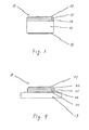
- Figs. 1 to 4 show cross-sectional views of four voltage-dependent resistors in accordance with this invention
- Figs. 5 and 6 show two typical voltage-current characteristics of such voltage-dependent resistors.
- the voltage-dependent resistor having the asymmetric voltage-current characteristics as shown in Fig. 5 is useful.
- the voltage-dependent resistor having the symmetric voltage-current characteristics as shown in Fig. 6 is useful.
- the non-ohmic property of this invention is supposed to be attributable to a tunnelling current through a barrier formed at an interface of the hetero-junction. Therefore, the non-ohmic property depends on the composition of metal oxide layer. Concerning the zinc oxide layer, any form is acceptable such as a sintered body, a deposited film and a single crystal, if the relative resistivity is adjusted to an appropriate value.
- a voltage-dependent resistor comprising a zinc oxide layer or two zinc oxide layers and a metal oxide layer comprising at least one member selected from the group consisting of cobalt oxide (Co203), manganese oxide (Mn0 2 ), barium oxide (BaO), strontium oxide (SrO), lead oxide (PbO) and rare earth oxides, with electrodes, has a non-ohmic property (voltage-dependent property) due to the heterojunction between the zinc oxide layer and the metal oxide layer.
- Zinc oxide and additives as shown in Tables 1 were mixed in a wet mill for 24 hours. Each of the mixtures was dried and pressed in a mold disc of 12 mm in diameter and 1.5 mm in thickness at a pressure of 250 kg/cm 2. The pressed bodies were sintered in air at 1250°C for 2 hours, and then furnace-cooled to room temperature. Each sintered body was lapped at the opposite surfaces thereof by aluminum oxide fine powder to the mirror surfaces. After cleaning, each lapped body was set in a chamber of high frequency sputtering equipment with a target having a composition as shown in Table 2.
- a metal oxide layer was deposited on the lapped body by the conventional high frequency sputtering method in the atmosphere of Ar and oxygen.
- the sputtering time was set at the best condition for each composition between 10 minutes and 3 hours.
- the atmosphere during sputtering was usually set at from 1.33 to 7.98 Pa (1 ⁇ 10 -2 torr to 6 ⁇ 10 -2 torr).
- the deposited metal oxide layer on the lapped body had almost the same composition as the target having the composition shown in Table 2.
- the high frequency sputtering method is as follows: a target and a substrate are set in a vacuum chamber opposedly. After introducing Ar gas (and oxygen) to an atmosphere of about 1.33 Pa (10- 2 torr), a high frequency, high voltage is applied between the target and the substrate so that plasma is generated between them. The activated Ar ions caused by the plasma bombard the target so that the constituent of the target is knocked out of it. Then the constituent is deposited on the substrate. This method is used to make a thin film on a substrate in the field of semiconductor devices.
- Each sputtered body was taken out of the chamber. Then aluminum electrodes were applied on the opposite surfaces of each sputtered body by the conventional vacuum deposition method.
- the resultant electroded devices had a structure as shown in Fig. 1, and the voltage-current characteristics as shown in Fig. 5, wherein the forward voltage-current characteristics was obtained when the electrode 4 on the zinc oxide body was biased positively.
- Table 3 shows that large n-values, low C-values and large capacitances are obtained, when said metal oxide layer comprises at least one of the members selected from the group consisting of cobalt oxide (C 02 0 3 ), manganese oxide (Mn0 2 ), barium oxide (BaO), strontium oxide (SrO), lead oxide (PbO) and rare earth oxides such as praseodymium oxide (Pr 2 0 3 ), neodymium oxide (Nd 2 0 3 ) and samarium oxide (Sm 2 0 3 ).
- cobalt oxide C 02 0 3
- manganese oxide Mn0 2
- barium oxide BaO
- strontium oxide SrO
- PbO lead oxide
- rare earth oxides such as praseodymium oxide (Pr 2 0 3 ), neodymium oxide (Nd 2 0 3 ) and samarium oxide (Sm 2 0 3 ).
- the electrical characteristics were improved by adding one of the members selected from the group of 0.001 to 0.1 mole percent of aluminum oxide (AI 2 0 3 ) and 0.001 to 0.1 mole percent of gallium oxide (Ga 2 0 3 ) to the zinc oxide layer.
- a glass substrate with an aluminum electrode was set in a vacuum chamber of high frequency sputtering equipment with a zinc oxide target having a composition as shown in Table 1. Then, a zinc oxide layer was deposited on the electrode by the high frequency sputtering method in Ar atmosphere. The sputtering time was set between 30 minutes and 3 hours. The atmosphere during sputtering was in an order of 1.33 Pa (10 -2 torr). The deposited zinc oxide layer on the electrode had almost the same composition as the target having the composition shown in Table 1.
- a metal oxide layer was deposited on it by using a different target having a composition as shown in Table 2 by the high frequency sputtering method described in Example 1. Each sputtered body was taken out of the chamber. Then an aluminum electrode was applied on the metal oxide layer by the vacuum deposition method described in Example 1.
- the resultant devices had a structure as shown in Fig. 2 and the voltage current characteristics as shown in Fig. 5, wherein the forward voltage-current characteristics were obtained when the electrode 10 on the glass substrate was based positively.
- the electrical characteristics of the resultant devices composed of a zinc oxide layer, a metal oxide layer, electrodes and a glass substrate are shown in Table 4, which shows C-values, n-values and capacitances.
- Table 4 shows that large n-values, low C-values and large capacitances when said metal oxide layer comprises at least one of the members selected from the group consisting of cobalt oxide (C 02 0 3 ), manganese oxide (Mn02), barium oxide (BaO), strontium oxide (SrO), lead oxide (PbO) and rare earth oxides such as praseodymium oxide (Pr 2 0 3 ), neodymium oxide (Nd 2 0 3 ) and samarium oxide (Sm 2 0 3 ).
- the electrical characteristics were improved by adding one of the members selected from the group of 0.001 to 0.1 mole percent of aluminum oxide (AI 2 0 3 ) and 0.001 to 0.1 mole percent of gallium oxide (Ga 2 0 3 ) to the zinc oxide layer.
- Zinc oxide sintered bodies having a composition as shown in Table 1 and a metal oxide layer having a composition as shown in Table 2 on the zinc oxide sintered bodies were made by the same process described in Example 1. Then a zinc oxide layer having a composition as shown in Table 1 was deposited on it by the same process described in Example 2. Then aluminum electrodes were applied on both zinc oxide layers as described in Example 2.
- Each device had a structure as shown in Fig. 3 and the voltage-current characteristics as shown in Fig. 6.
- the electrical characteristics of the resultant devices composed of a zinc oxide sintered body, a metal oxide layer and electrodes are shown in Table 5, which shows C-values, n-values and capacitances.
- Table 5 shows that large n-values, low C-values and large capacitances are obtained, when said metal oxide layer comprises at least one of the members selected from the group consisting of cobalt oxide (C 02 0 3 ), manganese oxide (Mn0 2 ), barium oxide (BaO), strontium oxide (SrO), lead oxide (PbO) and rare earth oxides such as praseodymium oxide (Pr 2 0 3 ), neodymium oxide (Nd 2 0 3 ) and samarium oxide (Sm 2 0 3 ).
- the electrical characteristics were improved by adding one of the members selected from the group consisting of 0.001 to 0.1 mole percent of aluminum oxide (A1 2 0 3 ) and 0.001 to 0.1 mole percent of gallium oxide (Ga 2 0 3 ) to the zinc oxide layer.
- a zinc oxide layer having a composition as shown in Table 1 on the aluminum electrode on a glass substrate and a metal oxide layer having a composition as shown in Table 2 on the zinc oxide layer was made by the same process described in Example 2. Then a zinc oxide layer having a composition as shown in Table 1 was deposited on it by the same process described in Example 2. Then an aluminum electrode was applied on the zinc oxide layer as described in Example 2.
- Each device had a structure as shown in Fig. 4 and the voltage-current characteristics as shown in Fig. 6, wherein the forward voltage-current characteristics were obtained when the electrode 23 on the glass substrate was biased positively.
- the electrical characteristics of the resultant devices composed of two zinc oxide layers, a metal oxide layer and electrodes are shown in Table 6, which shows C-values, n-values and capacitances.
- Table 6 shows that large n-values, low C-values and large capacitances are obtained, when said metal oxide layer comprises at least one of the members selected from the group consisting of cobalt oxide (Co 2 O 3 ), manganese oxide (Mn0 2 ), barium oxide (BaO), strontium oxide (SrO), lead oxide (PbO) and rare earth oxides such as praseodymium oxide (Pr 2 0 3 ), neodymium oxide (Nd 2 0 3 ) and samarium oxide (Sm 2 0 3 ).
- cobalt oxide Co 2 O 3
- manganese oxide Mn0 2
- barium oxide BaO
- strontium oxide SrO
- PbO lead oxide
- rare earth oxides such as praseodymium oxide (Pr 2 0 3 ), neodymium oxide (Nd 2 0 3 ) and samarium oxide (Sm 2 0 3 ).
- the electrical characteristics were improved by adding one of the members selected from the group consisting of 0.001 to 0.1 mole percent of aluminum oxide (AI 2 0 3 ) and 0.001 to 0.1 mole percent of gallium oxide (Ga 2 0 3 ) to the zinc oxide layer.
Landscapes
- Engineering & Computer Science (AREA)
- Microelectronics & Electronic Packaging (AREA)
- Physics & Mathematics (AREA)
- Electromagnetism (AREA)
- Compositions Of Oxide Ceramics (AREA)
- Thermistors And Varistors (AREA)
Claims (7)
Applications Claiming Priority (6)
| Application Number | Priority Date | Filing Date | Title |
|---|---|---|---|
| JP55060888A JPS6015131B2 (ja) | 1980-05-07 | 1980-05-07 | 電圧非直線抵抗器とその製造方法 |
| JP55060881A JPS6015129B2 (ja) | 1980-05-07 | 1980-05-07 | 電圧非直線抵抗器とその製造方法 |
| JP60888/80 | 1980-05-07 | ||
| JP55060882A JPS6015130B2 (ja) | 1980-05-07 | 1980-05-07 | 電圧非直線抵抗器とその製造方法 |
| JP60881/80 | 1980-05-07 | ||
| JP60882/80 | 1980-05-07 |
Publications (3)
| Publication Number | Publication Date |
|---|---|
| EP0040043A2 EP0040043A2 (fr) | 1981-11-18 |
| EP0040043A3 EP0040043A3 (en) | 1983-05-18 |
| EP0040043B1 true EP0040043B1 (fr) | 1985-08-28 |
Family
ID=27297320
Family Applications (1)
| Application Number | Title | Priority Date | Filing Date |
|---|---|---|---|
| EP81301998A Expired EP0040043B1 (fr) | 1980-05-07 | 1981-05-06 | Résistance dépendant de la tension |
Country Status (3)
| Country | Link |
|---|---|
| US (1) | US4383237A (fr) |
| EP (1) | EP0040043B1 (fr) |
| DE (1) | DE3171994D1 (fr) |
Families Citing this family (15)
| Publication number | Priority date | Publication date | Assignee | Title |
|---|---|---|---|---|
| US4477793A (en) * | 1982-06-30 | 1984-10-16 | Fuji Electric Co., Ltd. | Zinc oxide non-linear resistor |
| US4473812A (en) * | 1982-11-04 | 1984-09-25 | Fuji Electric Co., Ltd. | Voltage-dependent nonlinear resistor |
| US5004573A (en) * | 1989-11-02 | 1991-04-02 | Korea Institute Of Science And Technology | Fabrication method for high voltage zinc oxide varistor |
| EP0620567B1 (fr) * | 1989-11-08 | 1996-07-17 | Matsushita Electric Industrial Co., Ltd. | Varistor à l'oxyde de zinc, production de celui-ci et composition d'un verre cristallisé pour revêtement |
| JP2556151B2 (ja) * | 1989-11-21 | 1996-11-20 | 株式会社村田製作所 | 積層型バリスタ |
| US5124822A (en) * | 1990-05-08 | 1992-06-23 | Raychem Corporation | Varistor driven liquid crystal display |
| US5699035A (en) * | 1991-12-13 | 1997-12-16 | Symetrix Corporation | ZnO thin-film varistors and method of making the same |
| US5294374A (en) * | 1992-03-20 | 1994-03-15 | Leviton Manufacturing Co., Inc. | Electrical overstress materials and method of manufacture |
| EP0572151A3 (fr) * | 1992-05-28 | 1995-01-18 | Avx Corp | Varistors avec des connexions vaporisées cathodiquement et méthode pour déposer des connexions vaporisées cathodiquement sur des varistors. |
| US5565838A (en) * | 1992-05-28 | 1996-10-15 | Avx Corporation | Varistors with sputtered terminations |
| US5742223A (en) * | 1995-12-07 | 1998-04-21 | Raychem Corporation | Laminar non-linear device with magnetically aligned particles |
| JP4123957B2 (ja) * | 2003-02-10 | 2008-07-23 | 株式会社村田製作所 | 電圧依存性抵抗器 |
| US7642892B1 (en) * | 2006-03-10 | 2010-01-05 | Integrated Device Technology, Inc. | Negative voltage coefficient resistor and method of manufacture |
| KR20150109293A (ko) | 2014-03-19 | 2015-10-01 | 엔지케이 인슐레이터 엘티디 | 전압 비선형 저항 소자 및 그 제조 방법 |
| JP6703428B2 (ja) | 2016-03-28 | 2020-06-03 | 日本碍子株式会社 | 電圧非直線抵抗素子及びその製法 |
Family Cites Families (10)
| Publication number | Priority date | Publication date | Assignee | Title |
|---|---|---|---|---|
| US3412220A (en) * | 1963-11-26 | 1968-11-19 | Sprague Electric Co | Voltage sensitive switch and method of making |
| US3609469A (en) * | 1967-12-22 | 1971-09-28 | Charles Feldman | Voltage-controlled ionic variable resistor employing material transfer |
| JPS4814351B1 (fr) * | 1968-12-02 | 1973-05-07 | ||
| US3689863A (en) * | 1969-12-08 | 1972-09-05 | Matsushita Electric Industrial Co Ltd | Voltage dependent resistors in a surface barrier type |
| JPS5311075B2 (fr) * | 1973-02-09 | 1978-04-19 | ||
| JPS5070897A (fr) * | 1973-10-26 | 1975-06-12 | ||
| US3928242A (en) * | 1973-11-19 | 1975-12-23 | Gen Electric | Metal oxide varistor with discrete bodies of metallic material therein and method for the manufacture thereof |
| DE2553134A1 (de) * | 1975-11-24 | 1977-06-02 | Joachim Schneider | Dachabschluss-profilleiste |
| US4046847A (en) * | 1975-12-22 | 1977-09-06 | General Electric Company | Process for improving the stability of sintered zinc oxide varistors |
| US4272754A (en) * | 1979-12-17 | 1981-06-09 | General Electric Company | Thin film varistor |
-
1981
- 1981-05-05 US US06/260,720 patent/US4383237A/en not_active Expired - Lifetime
- 1981-05-06 DE DE8181301998T patent/DE3171994D1/de not_active Expired
- 1981-05-06 EP EP81301998A patent/EP0040043B1/fr not_active Expired
Also Published As
| Publication number | Publication date |
|---|---|
| DE3171994D1 (en) | 1985-10-03 |
| EP0040043A3 (en) | 1983-05-18 |
| US4383237A (en) | 1983-05-10 |
| EP0040043A2 (fr) | 1981-11-18 |
Similar Documents
| Publication | Publication Date | Title |
|---|---|---|
| US4400683A (en) | Voltage-dependent resistor | |
| EP0040043B1 (fr) | Résistance dépendant de la tension | |
| US4436650A (en) | Low voltage ceramic varistor | |
| JP4082696B2 (ja) | 積層型電子部品及びその製造方法 | |
| US4460623A (en) | Method of varistor capacitance reduction by boron diffusion | |
| EP0358323A1 (fr) | Résistances non linéaires dépendant de la tension | |
| EP0875067B1 (fr) | Methode de production d'un element de protection polyvalent | |
| JP2789714B2 (ja) | 電圧依存性非直線抵抗体磁器組成物およびバリスタの製造方法 | |
| JP2830322B2 (ja) | 電圧依存性非直線抵抗体磁器組成物およびバリスタの製造方法 | |
| JP2727693B2 (ja) | 電圧依存性非直線抵抗体磁器組成物およびバリスタの製造方法 | |
| JP2822612B2 (ja) | バリスタの製造方法 | |
| JP2800268B2 (ja) | 電圧依存性非直線抵抗体磁器組成物およびバリスタの製造方法 | |
| JP2789675B2 (ja) | 電圧依存性非直線抵抗体磁器組成物およびバリスタの製造方法 | |
| JPH05283208A (ja) | 積層型バリスタ | |
| JP2808777B2 (ja) | バリスタの製造方法 | |
| JP2789674B2 (ja) | 電圧依存性非直線抵抗体磁器組成物およびバリスタの製造方法 | |
| JP2548278B2 (ja) | 電圧依存性非直線抵抗体磁器組成物 | |
| JPS6236607B2 (fr) | ||
| JP2548279B2 (ja) | 電圧依存性非直線抵抗体磁器組成物 | |
| JP2789676B2 (ja) | 電圧依存性非直線抵抗体磁器組成物およびバリスタの製造方法 | |
| JP2808778B2 (ja) | バリスタの製造方法 | |
| JPS5910042B2 (ja) | 電圧非直線抵抗器 | |
| JP2548277B2 (ja) | 電圧依存性非直線抵抗体磁器組成物 | |
| JPH0682564B2 (ja) | 電圧依存性非直線抵抗体磁器組成物 | |
| JPH0740522B2 (ja) | 電圧依存性非直線抵抗体磁器組成物 |
Legal Events
| Date | Code | Title | Description |
|---|---|---|---|
| PUAI | Public reference made under article 153(3) epc to a published international application that has entered the european phase |
Free format text: ORIGINAL CODE: 0009012 |
|
| AK | Designated contracting states |
Designated state(s): DE FR GB NL |
|
| PUAL | Search report despatched |
Free format text: ORIGINAL CODE: 0009013 |
|
| AK | Designated contracting states |
Designated state(s): DE FR GB NL |
|
| 17P | Request for examination filed |
Effective date: 19831117 |
|
| GRAA | (expected) grant |
Free format text: ORIGINAL CODE: 0009210 |
|
| AK | Designated contracting states |
Designated state(s): DE FR GB NL |
|
| REF | Corresponds to: |
Ref document number: 3171994 Country of ref document: DE Date of ref document: 19851003 |
|
| PLBE | No opposition filed within time limit |
Free format text: ORIGINAL CODE: 0009261 |
|
| STAA | Information on the status of an ep patent application or granted ep patent |
Free format text: STATUS: NO OPPOSITION FILED WITHIN TIME LIMIT |
|
| EN | Fr: translation not filed | ||
| 26N | No opposition filed | ||
| PGFP | Annual fee paid to national office [announced via postgrant information from national office to epo] |
Ref country code: GB Payment date: 19940426 Year of fee payment: 14 |
|
| PGFP | Annual fee paid to national office [announced via postgrant information from national office to epo] |
Ref country code: FR Payment date: 19940511 Year of fee payment: 14 Ref country code: DE Payment date: 19940511 Year of fee payment: 14 |
|
| PGFP | Annual fee paid to national office [announced via postgrant information from national office to epo] |
Ref country code: NL Payment date: 19940531 Year of fee payment: 14 |
|
| PG25 | Lapsed in a contracting state [announced via postgrant information from national office to epo] |
Ref country code: GB Effective date: 19950506 |
|
| PG25 | Lapsed in a contracting state [announced via postgrant information from national office to epo] |
Ref country code: NL Effective date: 19951201 |
|
| GBPC | Gb: european patent ceased through non-payment of renewal fee |
Effective date: 19950506 |
|
| NLV4 | Nl: lapsed or anulled due to non-payment of the annual fee |
Effective date: 19951201 |
|
| PG25 | Lapsed in a contracting state [announced via postgrant information from national office to epo] |
Ref country code: DE Effective date: 19960201 |
|
| PG25 | Lapsed in a contracting state [announced via postgrant information from national office to epo] |
Ref country code: FR Effective date: 19960229 |
|
| REG | Reference to a national code |
Ref country code: FR Ref legal event code: ST |
|
| REG | Reference to a national code |
Ref country code: FR Ref legal event code: ST |