EP0040377B1 - Integrierte Schaltung zum Lesen und Schreiben von Informationen - Google Patents
Integrierte Schaltung zum Lesen und Schreiben von Informationen Download PDFInfo
- Publication number
- EP0040377B1 EP0040377B1 EP81103540A EP81103540A EP0040377B1 EP 0040377 B1 EP0040377 B1 EP 0040377B1 EP 81103540 A EP81103540 A EP 81103540A EP 81103540 A EP81103540 A EP 81103540A EP 0040377 B1 EP0040377 B1 EP 0040377B1
- Authority
- EP
- European Patent Office
- Prior art keywords
- region
- source
- type
- substrate
- voltage
- Prior art date
- Legal status (The legal status is an assumption and is not a legal conclusion. Google has not performed a legal analysis and makes no representation as to the accuracy of the status listed.)
- Expired
Links
- 239000000758 substrate Substances 0.000 claims description 68
- 239000004065 semiconductor Substances 0.000 claims description 34
- 239000012212 insulator Substances 0.000 claims description 21
- 239000012535 impurity Substances 0.000 claims description 16
- 230000005669 field effect Effects 0.000 claims description 13
- 230000000295 complement effect Effects 0.000 claims description 7
- 239000011159 matrix material Substances 0.000 claims description 3
- VYPSYNLAJGMNEJ-UHFFFAOYSA-N Silicium dioxide Chemical compound O=[Si]=O VYPSYNLAJGMNEJ-UHFFFAOYSA-N 0.000 description 10
- XAGFODPZIPBFFR-UHFFFAOYSA-N aluminium Chemical compound [Al] XAGFODPZIPBFFR-UHFFFAOYSA-N 0.000 description 8
- 229910052782 aluminium Inorganic materials 0.000 description 8
- 239000004411 aluminium Substances 0.000 description 8
- 238000003491 array Methods 0.000 description 6
- 239000002784 hot electron Substances 0.000 description 5
- 235000012239 silicon dioxide Nutrition 0.000 description 5
- 239000000377 silicon dioxide Substances 0.000 description 5
- 238000010521 absorption reaction Methods 0.000 description 4
- 230000003071 parasitic effect Effects 0.000 description 3
- 229910021420 polycrystalline silicon Inorganic materials 0.000 description 3
- 230000006399 behavior Effects 0.000 description 2
- 230000015556 catabolic process Effects 0.000 description 2
- 230000000694 effects Effects 0.000 description 2
- 230000005684 electric field Effects 0.000 description 2
- 230000010354 integration Effects 0.000 description 2
- 238000004519 manufacturing process Methods 0.000 description 2
- XUIMIQQOPSSXEZ-UHFFFAOYSA-N Silicon Chemical compound [Si] XUIMIQQOPSSXEZ-UHFFFAOYSA-N 0.000 description 1
- 239000000969 carrier Substances 0.000 description 1
- 238000007796 conventional method Methods 0.000 description 1
- 230000003247 decreasing effect Effects 0.000 description 1
- 230000001419 dependent effect Effects 0.000 description 1
- 238000010586 diagram Methods 0.000 description 1
- XUFQPHANEAPEMJ-UHFFFAOYSA-N famotidine Chemical compound NC(N)=NC1=NC(CSCCC(N)=NS(N)(=O)=O)=CS1 XUFQPHANEAPEMJ-UHFFFAOYSA-N 0.000 description 1
- 238000002955 isolation Methods 0.000 description 1
- 238000000034 method Methods 0.000 description 1
- 229910052710 silicon Inorganic materials 0.000 description 1
- 239000010703 silicon Substances 0.000 description 1
Images


Classifications
-
- G—PHYSICS
- G11—INFORMATION STORAGE
- G11C—STATIC STORES
- G11C16/00—Erasable programmable read-only memories
- G11C16/02—Erasable programmable read-only memories electrically programmable
- G11C16/04—Erasable programmable read-only memories electrically programmable using variable threshold transistors, e.g. FAMOS
- G11C16/0408—Erasable programmable read-only memories electrically programmable using variable threshold transistors, e.g. FAMOS comprising cells containing floating gate transistors
- G11C16/0416—Erasable programmable read-only memories electrically programmable using variable threshold transistors, e.g. FAMOS comprising cells containing floating gate transistors comprising cells containing a single floating gate transistor and no select transistor, e.g. UV EPROM
-
- H—ELECTRICITY
- H10—SEMICONDUCTOR DEVICES; ELECTRIC SOLID-STATE DEVICES NOT OTHERWISE PROVIDED FOR
- H10B—ELECTRONIC MEMORY DEVICES
- H10B41/00—Electrically erasable-and-programmable ROM [EEPROM] devices comprising floating gates
-
- H—ELECTRICITY
- H10—SEMICONDUCTOR DEVICES; ELECTRIC SOLID-STATE DEVICES NOT OTHERWISE PROVIDED FOR
- H10D—INORGANIC ELECTRIC SEMICONDUCTOR DEVICES
- H10D84/00—Integrated devices formed in or on semiconductor substrates that comprise only semiconducting layers, e.g. on Si wafers or on GaAs-on-Si wafers
- H10D84/80—Integrated devices formed in or on semiconductor substrates that comprise only semiconducting layers, e.g. on Si wafers or on GaAs-on-Si wafers characterised by the integration of at least one component covered by groups H10D12/00 or H10D30/00, e.g. integration of IGFETs
- H10D84/82—Integrated devices formed in or on semiconductor substrates that comprise only semiconducting layers, e.g. on Si wafers or on GaAs-on-Si wafers characterised by the integration of at least one component covered by groups H10D12/00 or H10D30/00, e.g. integration of IGFETs of only field-effect components
- H10D84/83—Integrated devices formed in or on semiconductor substrates that comprise only semiconducting layers, e.g. on Si wafers or on GaAs-on-Si wafers characterised by the integration of at least one component covered by groups H10D12/00 or H10D30/00, e.g. integration of IGFETs of only field-effect components of only insulated-gate FETs [IGFET]
- H10D84/85—Complementary IGFETs, e.g. CMOS
- H10D84/854—Complementary IGFETs, e.g. CMOS comprising arrangements for preventing bipolar actions between the different IGFET regions, e.g. arrangements for latchup prevention
Definitions
- This invention relates to an integrated circuit device for writing and reading information which includes non-volatile memory elements and complementary insulated-gate type field effect transistors.
- Insulated-gate type field effect transistors which have a SAMOS structure or a MNOS structure are well-known as non-volatile memory elements.
- a large number of memory elements of these kinds are integrated on a semiconductor substrate ordinarily like a matrix.
- a "1” or "0” is selectively written into each of the memory elements and is read out from the same by a control circuit formed therearound.
- Such an integrated circuit device is desired to have less power consumption in order to suppress heat production.
- CMOS devices complementary insulated-gate type field effect transistors
- CMOS device complementary insulated-gate type field effect transistors
- a CMOS device comprise a N-type semiconductor substrate, a P-type well region formed in the substrate, a N-channel MOS transistor formed on the well region and a P-channel MOS transistor formed on the substrate; wherein the gate electrodes of the N-channel and P-channel transistors are commonly connected, thereby constituting an input terminal and the drain regions of both transistors are commonly connected, thereby constituting an output terminal. While a predetermined voltage is applied between the two source regions of both transistors, the CMOS device operates as an inverter.
- the above mentioned CMOS device has essentially a PNPN structure comprising the source of the P-channel MOS transistor, the N-type semiconductor substrate, the P-type well region and the source of the N-channel MOS transistor. It is possible that the PNPN structure works as a thyristor and then a circuit between the sources of the two transistors is short-circuited due to a noise signal being introduced into the PNPN structure, so that the control circuit of the CMOS devices may cause an error behaviour or may be broken in the worst case. Such a phenomenon that a parastic thyristor is wrongly turned on is called "Latch-up". This Latch-up phenomenon can be essentially caused also in the case that both non-volatile memory elements and CMOS devices are formed together on a same semiconductor substrate.
- a consideration for preventing the Latch-up phenomenon of CMOS devices is disclosed in DENSHI TSUSHIN GAKKAI RONBUNSHI Vol. J61-C, No. 2, 1978, PP. 106-113.
- the following concrete means are shown as countermeasures for the Latch-up phenomenon.
- One of the means is to isolate electrically the P-channel MOS transistors and the N-channel MOS transistors by forming insulator layers therebetween.
- Another of the means is to cut off electric channels between the P-channel MOS transistors and the P-type well regions by forming P-type regions of a low impurity concentration therebetween.
- Yet another of the means is to determine the mutual positional relation between the P-channel transistors and the N-channel transistors in order to prevent thyristor action of the CMOS devices, JP-A-55 15 222. Yet another of the means is to determine the electric characteristics of the N-channel and P-channel transistors so as to prevent thyristor action of the CMOS devices.
- these countermeasures bring inevitably lower integration density, more complicated manufacturing processes or worse performance of the CMOS devices as inverters.
- This integrated circuit device has a high integration density and a superior inverter performance of complementary insulated-gate type field effect transistors and can be fabricated with ease.
- a predetermined voltage for example a ground voltage or a negative voltage
- the second semiconductor region is connected to the voltage source terminal.
- the impurity concentration of the second semiconductor region is desired to be from 1 x 10 2 ° cm- 3 to 1 x 10 22 cm- 3 so as to have a good contact with an electrode, to which the predetermined voltage is applied.
- the second semiconductor region can be obviously distinguished from a semiconductor region of one conductivity type which is formed conventionally in a semiconductor substrate of one conductivity type, for the purpose of preventing leakage of current from MOS transistors which may be caused by what is called the inversion phenomenon. Namely the conventional semiconductor region, to which any voltage is never directly applied, has ordinarily an impurity concentration order of 10" cm- 3 .
- CMOS devices complementary insulated-gate type field effect transistors
- Practically information is stored into an insulated-gate type field effect transistor (a non-volatile memory element) with a SAMOS structure or a MNOS structure according to the following operation.
- electrons or holes are produced through collision of accelerated carriers with atoms.
- the electrons or holes are injected into traps existing between a semiconductor substrate and a control electrode of the transistor. Then the traps store the information.
- CMOS devices At the same time, a substrate current which has been produced near by the non-volatile memory elements flows into the CMOS devices. Then the parastic thyristors of the CMOS devices are turned on, so that the CMOS devices may operate in an error manner or may be broken themselves by an overcurrent.
- the substrate current is absorbed through applying a predetermined voltage directly to at least one semiconductor region of one conductivity type, which has an impurity concentration higher than that of the semiconductor substrate and which is formed between the non-volatile memory elements and the CMOS devices.
- the Latch-up phenomenon of the CMOS devices is decreased very much without changing the CMOS structures themselves.
- memory arrays 2, 3 are formed on a semiconductor substrate 1 of P conductivity type of a 2 x 10 14 cm- 3 impurity concentration.
- the memory arrays 2, 3 are constituted by insulated-gate field effect transistors of a SAMOS structure.
- Each memory array 2, 3 consists of four memory blocks and in each of the memory blocks, there is formed like a matrix a circuit of insulated-gate field effect transistors (MOS transistors) 4A to 4Z with a SAMOS structure as shown in Fig. 2.
- Circuits 5 to 12 which include plural sets of two complementary insulated-gate field effect transistors (CMOS devices) are formed around the memory arrays 2, 3 in order to control writing information into the transistors 4A to 4Z and reading out the information therefrom.
- CMOS devices complementary insulated-gate field effect transistors
- bonding pads 13 to 36 are formed on insulator films which cover the substrate 1 around the circuit 5 to 12.
- the bonding pads are utilized as power source terminals, input terminals and output terminals respectively.
- Each of the CMOS devices which constitute the circuits 5 to 12 consists of a P-channel type MOS transistor and a N-channel type MOS transistor. A predetermined voltage is applied between the sources of the two transistors. The gates of the two transistors are connected commonly, thereby forming an input terminal. The drains of the two transistors are connected commonly, thereby forming an output terminal.
- CMOS devices work as inverters.
- Row address signals are sent into a row address buffer circuit 12 through the pads 13 to 16 and the pads 33 to 35.
- the row address signals are converted into driving signals for a row decoder and row selecting circuit 5.
- column address signals are sent into a column address buffer circuit 6 through the pads 17 to 20.
- the column address signals are converted into driving signals for a column decoder circuit 9.
- Data signals are provided to a data input and output buffer circuit 10 through the pads 21 to 23 and the pads 25 to 29.
- This circuit 10 selects each of 8 blocks in the memory arrays 2, 3 one after another. In a selected block, one of the non-volatile memory transistors is designated by the row decoder and row selecting circuit 5 and the column selecting circuit 7, 8 which are controlled by the signals from the column decoder circuit 9. Then a "1" or "0” is written into the designated non-volatile memory transistor (or therefrom a "1" or "0” is read out).
- Control of writing and reading is carried out by a control circuit 11 which receives control signals from the pads 30 to 32.
- a power source voltage is applied to the pad 36.
- a ground voltage is applied to the pad 24.
- Long and narrow regions 40, 41 are formed in a surface region of the semiconductor substrate 1 around said memory arrays 2, 3.
- the regions 40, 41 to which a ground voltage is applied through the pad 24, have P-conductivity type and a 4 x 10 21 cm- 3 impurity concentration.
- Fig. 3 is a magnified cross-sectional view taken along line A-A in Fig. 1.
- a well region 43 of N-conductivity type having a 6 x 10 15 cm- 3 impurity concentration is formed in the P-type semiconductor substrate 1.
- a N-type region 44 of a 4 x 10 2 ' cm- 3 impurity concentration there is formed a P-type source region 46 and a P-type drain region 47 respectively having a 4 x 10" cm- 3 impurity concentration and these regions constituting a P-channel type MOS transistor 45.
- An insulator film 48 of silicon dioxide is formed between the source region 46 and the drain region 47 on the N-type region 43. Further, a poly-silicon gate electrode 49 is formed on the insulator film 48.
- a P-type region 56 of a 4 x 10 11 cm- 3 impurity concentration is formed adjoining the source region 51 in the N-type surface region of the substrate 1. It is not always necessary that the region 56 is brought into contact with the source region 51.
- the P-type region 56 and the N-type source region 51 are connected commonly to an aluminium electrode 57, to which a ground voltage Vss is applied.
- the substrate 1 is grounded through the electrode 57.
- the N-type region 44 in the N-type well region 43 and the P-type source region 46 of the transistor 45 are connected commonly to an aluminium electrode 58, to which a voltage of +5 V is applied.
- the N-type well region 43 is kept at a positive potential through the N-type region 44 and the electrode 58. Accordingly, the P-N junction between the N-type well region 43 and the P-type substrate 1 is backward-biased and the region 43 and the substrate 1 are electrically isolated from each other.
- the gate electrodes 49, 54 of the transistors 45, 50 are connected commonly to an aluminium electrode 60 and the drain regions 47, 52 of the transistors 45, 50 are connected commonly to an aluminium electrode 61.
- An input signal Vi for a CMOS device 62 which consists of the two transistors 45, 50 is supplied to the electrode 60, and the CMOS device 62 operates as an inverter.
- An output signal Vo is obtained from the electrode 61.
- An insulator film 68 of silicon dioxide is formed between the source region 66 and the drain region 67 on the substrate 1.
- a floating-gate electrode 69 of poly-silicon is disposed on the insulator film 68.
- a control-gate electrode 71 is formed on the insulator film 70.
- the control-gate electrode 71 is connected to an aluminium electrode 72, to which a gate-control voltage V G is applied.
- the source region 66 is connected to an aluminium electrode 73, to which a ground voltage Vss is applied.
- the drain region 67 is connected to an aluminium electrode 74, to which a drain-control voltage V D is applied.
- These hot electrons are injected into the floating-gate electrode 69 and/or the boundary face between the electrode 69 and the insulator film 68 by the electric field between the control-gate electrode 71 and the substrate 1, and then the hot electrons are trapped.
- the writing operation is performed and a substrate current is formed by the holes which have been produced simultaneously. If a voltage higher that the above voltage (+20 - +21 Volt) is applied to the drain electrode 74, an avalanche break-down occurs at the P-N junction between the drain region 67 and the substrate 1, so that hot electrons and holes are produced. Then, these hot electrons are directly injected into the floating-gate electrode 69 and/or the boundary face between the electrode 69 and the insulator film 68.
- ultraviolet rays should be applied to the gate region of the transistor 65 or -50 to -60 Volt should be applied to the control-gate electrode 72.
- the above-mentioned P-type region 40 is formed in a surface region of the substrate 1 between the non-volatile memory transistor 65 and the CMOS device 62.
- the P-type region 40 has an impurity concentration of 4 x 10 21 cm- 3 and is connected to an aluminium electrode 80, to which a ground voltage is applied.
- the surface of the substrate 1 is covered with an insulator film 81 of silicon dioxide. In the insulator film 81, contact holes for the electrodes are selectively formed.
- An integrated circuit device of the above structure can be fabricated through conventional methods. In the above mentioned device, holes flow in the substrate 1 on the writing operation, and then a substrate current I suB is formed.
- a P-N junction between the N-type well region 43 and the source region 46 will be forward-biased so that holes will be injected from the source region 46 through the N-type well region 43 and the P-type substrate 1 into the N-type source region 51.
- a great value current will begin to flow between the electrodes 58, 57 on account of positive feedback effect of the parasitic thyristor, which has a PNPN structure comprising the P-type source region 46 of the transistor 45, the N-type well region 43, the P-type substrate 1 and the N-type source region 51 of the transistor 50.
- This Latch-up phenomenon is caused only under the condition that a substrate current flows in the substrate and independently of whether or not the P-type region 56 exists around the CMOS device 62.
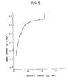
- Fig. 5 shows a relation between substrate current values I suB and current values too of the current which flows into the source electrode 58 in accordance with a conventional device, wherein the P-type region 40 does not exist in the substrate 1. From the curve in Fig. 5 it is well understood that when the substrate current I suB comes to have a great value more than 1.12 mA, the parastic thyristor is turned on and the current top increases abruptly.
- the P-type region of a high impurity concentration for substrate current absorption is allowed to have a shape similar to a loop with a crack as shown with a reference mark "41" in Fig. 1.
Landscapes
- Engineering & Computer Science (AREA)
- Microelectronics & Electronic Packaging (AREA)
- Metal-Oxide And Bipolar Metal-Oxide Semiconductor Integrated Circuits (AREA)
- Non-Volatile Memory (AREA)
- Semiconductor Memories (AREA)
Claims (5)
Applications Claiming Priority (2)
| Application Number | Priority Date | Filing Date | Title |
|---|---|---|---|
| JP6624580A JPS56162860A (en) | 1980-05-19 | 1980-05-19 | Semiconductor device |
| JP66245/80 | 1980-05-19 |
Publications (3)
| Publication Number | Publication Date |
|---|---|
| EP0040377A2 EP0040377A2 (de) | 1981-11-25 |
| EP0040377A3 EP0040377A3 (en) | 1983-10-26 |
| EP0040377B1 true EP0040377B1 (de) | 1986-09-03 |
Family
ID=13310284
Family Applications (1)
| Application Number | Title | Priority Date | Filing Date |
|---|---|---|---|
| EP81103540A Expired EP0040377B1 (de) | 1980-05-19 | 1981-05-08 | Integrierte Schaltung zum Lesen und Schreiben von Informationen |
Country Status (4)
| Country | Link |
|---|---|
| US (1) | US4692785A (de) |
| EP (1) | EP0040377B1 (de) |
| JP (1) | JPS56162860A (de) |
| DE (1) | DE3175254D1 (de) |
Families Citing this family (10)
| Publication number | Priority date | Publication date | Assignee | Title |
|---|---|---|---|---|
| EP0109854A3 (de) * | 1982-11-23 | 1985-08-07 | American Microsystems, Incorporated | Halbleiterspeicheranordnungen und deren Herstellungsverfahren |
| EP0138439B1 (de) * | 1983-09-28 | 1990-12-19 | Kabushiki Kaisha Toshiba | Elektrisch löschbare und programmierbare nichtflüchtige Halbleiterspeicheranordnung mit zwei Gate-Elektroden |
| JPS60225459A (ja) * | 1984-04-23 | 1985-11-09 | Nec Corp | 半導体集積回路 |
| WO1996036050A1 (en) * | 1995-05-12 | 1996-11-14 | Advanced Micro Devices, Inc. | Sector architecture for flash memory device |
| US7042027B2 (en) * | 2002-08-30 | 2006-05-09 | Micron Technology, Inc. | Gated lateral thyristor-based random access memory cell (GLTRAM) |
| US6888200B2 (en) * | 2002-08-30 | 2005-05-03 | Micron Technology Inc. | One transistor SOI non-volatile random access memory cell |
| US8125003B2 (en) * | 2003-07-02 | 2012-02-28 | Micron Technology, Inc. | High-performance one-transistor memory cell |
| US7224002B2 (en) * | 2004-05-06 | 2007-05-29 | Micron Technology, Inc. | Silicon on insulator read-write non-volatile memory comprising lateral thyristor and trapping layer |
| US7145186B2 (en) * | 2004-08-24 | 2006-12-05 | Micron Technology, Inc. | Memory cell with trenched gated thyristor |
| US11817449B2 (en) * | 2021-04-29 | 2023-11-14 | Macronix International Co., Ltd. | Memory devices with discharging circuits |
Family Cites Families (7)
| Publication number | Priority date | Publication date | Assignee | Title |
|---|---|---|---|---|
| US3971001A (en) * | 1974-06-10 | 1976-07-20 | Sperry Rand Corporation | Reprogrammable read only variable threshold transistor memory with isolated addressing buffer |
| US3955210A (en) * | 1974-12-30 | 1976-05-04 | International Business Machines Corporation | Elimination of SCR structure |
| US4149176A (en) * | 1975-07-18 | 1979-04-10 | Tokyo Shibaura Electric Co., Ltd. | Complementary MOSFET device |
| US4152717A (en) * | 1975-07-18 | 1979-05-01 | Tokyo Shibaura Electric Co., Ltd. | Complementary MOSFET device |
| US4167747A (en) * | 1975-07-18 | 1979-09-11 | Tokyo Shibaura Electric Co., Ltd. | Complementary mosfet device and method of manufacturing the same |
| JPS5211874A (en) * | 1975-07-18 | 1977-01-29 | Toshiba Corp | Semiconductor device |
| JPS5939904B2 (ja) * | 1978-09-28 | 1984-09-27 | 株式会社東芝 | 半導体装置 |
-
1980
- 1980-05-19 JP JP6624580A patent/JPS56162860A/ja active Pending
-
1981
- 1981-05-08 EP EP81103540A patent/EP0040377B1/de not_active Expired
- 1981-05-08 DE DE8181103540T patent/DE3175254D1/de not_active Expired
- 1981-05-13 US US06/263,252 patent/US4692785A/en not_active Expired - Lifetime
Also Published As
| Publication number | Publication date |
|---|---|
| EP0040377A3 (en) | 1983-10-26 |
| US4692785A (en) | 1987-09-08 |
| JPS56162860A (en) | 1981-12-15 |
| EP0040377A2 (de) | 1981-11-25 |
| DE3175254D1 (en) | 1986-10-09 |
Similar Documents
| Publication | Publication Date | Title |
|---|---|---|
| US6423584B2 (en) | method for forming capacitors and field effect transistors in a semiconductor integrated circuit device | |
| US4742492A (en) | EEPROM memory cell having improved breakdown characteristics and driving circuitry therefor | |
| US4672409A (en) | Nonvolatile semiconductor memory device | |
| US6312990B1 (en) | Structure nonvolatile semiconductor memory cell array and method for fabricating same | |
| US6740958B2 (en) | Semiconductor memory device | |
| JP2821667B2 (ja) | 集積回路チップ | |
| US4939558A (en) | EEPROM memory cell and driving circuitry | |
| US5553016A (en) | Semiconductor memory device | |
| US4663740A (en) | High speed eprom cell and array | |
| US6606265B2 (en) | Common source EEPROM and flash memory | |
| US4692785A (en) | Integrated circuit device for writing and reading information | |
| US4503524A (en) | Electrically erasable dual-injector floating gate programmable memory device | |
| US4654825A (en) | E2 prom memory cell | |
| US5172198A (en) | MOS type semiconductor device | |
| KR860000159B1 (ko) | 반도체 메모리 | |
| EP0946988B1 (de) | Speicherredundanzschaltung, die einzelne polysilizium-schwebegattertransistoren als redundanzelemente verwendet | |
| US4237472A (en) | High performance electrically alterable read only memory (EAROM) | |
| US5650956A (en) | Current amplification type mask-ROM | |
| EP0292327A2 (de) | Schutzschaltungen gegen elektrostatischen Durchbruch | |
| US4586065A (en) | MNOS memory cell without sidewalk | |
| US7317633B2 (en) | Protection of NROM devices from charge damage | |
| JPS6057673A (ja) | Mos型半導体装置 | |
| US5519244A (en) | Semiconductor device having aligned semiconductor regions and a plurality of MISFETs | |
| US4143390A (en) | Semiconductor device and a logical circuit formed of the same | |
| US6424000B1 (en) | Floating gate memory apparatus and method for selected programming thereof |
Legal Events
| Date | Code | Title | Description |
|---|---|---|---|
| PUAI | Public reference made under article 153(3) epc to a published international application that has entered the european phase |
Free format text: ORIGINAL CODE: 0009012 |
|
| AK | Designated contracting states |
Designated state(s): DE FR GB NL |
|
| PUAL | Search report despatched |
Free format text: ORIGINAL CODE: 0009013 |
|
| AK | Designated contracting states |
Designated state(s): DE FR GB NL |
|
| 17P | Request for examination filed |
Effective date: 19831223 |
|
| RAP1 | Party data changed (applicant data changed or rights of an application transferred) |
Owner name: KABUSHIKI KAISHA TOSHIBA |
|
| GRAA | (expected) grant |
Free format text: ORIGINAL CODE: 0009210 |
|
| AK | Designated contracting states |
Kind code of ref document: B1 Designated state(s): DE FR GB |
|
| ET | Fr: translation filed | ||
| REF | Corresponds to: |
Ref document number: 3175254 Country of ref document: DE Date of ref document: 19861009 |
|
| PLBE | No opposition filed within time limit |
Free format text: ORIGINAL CODE: 0009261 |
|
| STAA | Information on the status of an ep patent application or granted ep patent |
Free format text: STATUS: NO OPPOSITION FILED WITHIN TIME LIMIT |
|
| 26N | No opposition filed | ||
| PGFP | Annual fee paid to national office [announced via postgrant information from national office to epo] |
Ref country code: GB Payment date: 19970429 Year of fee payment: 17 |
|
| PGFP | Annual fee paid to national office [announced via postgrant information from national office to epo] |
Ref country code: FR Payment date: 19970513 Year of fee payment: 17 |
|
| PGFP | Annual fee paid to national office [announced via postgrant information from national office to epo] |
Ref country code: DE Payment date: 19970516 Year of fee payment: 17 |
|
| PG25 | Lapsed in a contracting state [announced via postgrant information from national office to epo] |
Ref country code: GB Free format text: LAPSE BECAUSE OF NON-PAYMENT OF DUE FEES Effective date: 19980508 |
|
| PG25 | Lapsed in a contracting state [announced via postgrant information from national office to epo] |
Ref country code: FR Free format text: LAPSE BECAUSE OF NON-PAYMENT OF DUE FEES Effective date: 19980531 |
|
| GBPC | Gb: european patent ceased through non-payment of renewal fee |
Effective date: 19980508 |
|
| PG25 | Lapsed in a contracting state [announced via postgrant information from national office to epo] |
Ref country code: DE Free format text: LAPSE BECAUSE OF NON-PAYMENT OF DUE FEES Effective date: 19990302 |
|
| REG | Reference to a national code |
Ref country code: FR Ref legal event code: ST |