EP0138439B1 - Elektrisch löschbare und programmierbare nichtflüchtige Halbleiterspeicheranordnung mit zwei Gate-Elektroden - Google Patents
Elektrisch löschbare und programmierbare nichtflüchtige Halbleiterspeicheranordnung mit zwei Gate-Elektroden Download PDFInfo
- Publication number
- EP0138439B1 EP0138439B1 EP84306502A EP84306502A EP0138439B1 EP 0138439 B1 EP0138439 B1 EP 0138439B1 EP 84306502 A EP84306502 A EP 84306502A EP 84306502 A EP84306502 A EP 84306502A EP 0138439 B1 EP0138439 B1 EP 0138439B1
- Authority
- EP
- European Patent Office
- Prior art keywords
- region
- semiconductor region
- data updating
- semiconductor
- potential
- Prior art date
- Legal status (The legal status is an assumption and is not a legal conclusion. Google has not performed a legal analysis and makes no representation as to the accuracy of the status listed.)
- Expired
Links
- 239000004065 semiconductor Substances 0.000 title claims description 113
- 230000015654 memory Effects 0.000 claims description 56
- 239000000758 substrate Substances 0.000 claims description 46
- 230000000694 effects Effects 0.000 claims description 15
- 239000011159 matrix material Substances 0.000 claims description 7
- 230000002093 peripheral effect Effects 0.000 claims description 7
- VYPSYNLAJGMNEJ-UHFFFAOYSA-N Silicium dioxide Chemical compound O=[Si]=O VYPSYNLAJGMNEJ-UHFFFAOYSA-N 0.000 claims description 5
- 229910052814 silicon oxide Inorganic materials 0.000 claims description 3
- XUIMIQQOPSSXEZ-UHFFFAOYSA-N Silicon Chemical compound [Si] XUIMIQQOPSSXEZ-UHFFFAOYSA-N 0.000 claims description 2
- 229910052594 sapphire Inorganic materials 0.000 claims description 2
- 239000010980 sapphire Substances 0.000 claims description 2
- 229910052710 silicon Inorganic materials 0.000 claims description 2
- 239000010703 silicon Substances 0.000 claims description 2
- 239000012212 insulator Substances 0.000 claims 4
- 230000015556 catabolic process Effects 0.000 description 24
- 238000009792 diffusion process Methods 0.000 description 13
- 238000002955 isolation Methods 0.000 description 11
- 230000005684 electric field Effects 0.000 description 6
- 239000012535 impurity Substances 0.000 description 5
- 238000000034 method Methods 0.000 description 4
- 230000001133 acceleration Effects 0.000 description 2
- 230000003247 decreasing effect Effects 0.000 description 2
- 238000005468 ion implantation Methods 0.000 description 2
- 238000004519 manufacturing process Methods 0.000 description 2
- OAICVXFJPJFONN-UHFFFAOYSA-N Phosphorus Chemical compound [P] OAICVXFJPJFONN-UHFFFAOYSA-N 0.000 description 1
- 229910052785 arsenic Inorganic materials 0.000 description 1
- RQNWIZPPADIBDY-UHFFFAOYSA-N arsenic atom Chemical compound [As] RQNWIZPPADIBDY-UHFFFAOYSA-N 0.000 description 1
- QVGXLLKOCUKJST-UHFFFAOYSA-N atomic oxygen Chemical compound [O] QVGXLLKOCUKJST-UHFFFAOYSA-N 0.000 description 1
- 238000010276 construction Methods 0.000 description 1
- 230000007423 decrease Effects 0.000 description 1
- 238000002347 injection Methods 0.000 description 1
- 239000007924 injection Substances 0.000 description 1
- 239000012299 nitrogen atmosphere Substances 0.000 description 1
- 229910052760 oxygen Inorganic materials 0.000 description 1
- 239000001301 oxygen Substances 0.000 description 1
- 238000012856 packing Methods 0.000 description 1
- 229910052698 phosphorus Inorganic materials 0.000 description 1
- 239000011574 phosphorus Substances 0.000 description 1
- 238000009751 slip forming Methods 0.000 description 1
Images

Classifications
-
- G—PHYSICS
- G11—INFORMATION STORAGE
- G11C—STATIC STORES
- G11C16/00—Erasable programmable read-only memories
- G11C16/02—Erasable programmable read-only memories electrically programmable
- G11C16/04—Erasable programmable read-only memories electrically programmable using variable threshold transistors, e.g. FAMOS
- G11C16/0408—Erasable programmable read-only memories electrically programmable using variable threshold transistors, e.g. FAMOS comprising cells containing floating gate transistors
- G11C16/0416—Erasable programmable read-only memories electrically programmable using variable threshold transistors, e.g. FAMOS comprising cells containing floating gate transistors comprising cells containing a single floating gate transistor and no select transistor, e.g. UV EPROM
-
- H—ELECTRICITY
- H10—SEMICONDUCTOR DEVICES; ELECTRIC SOLID-STATE DEVICES NOT OTHERWISE PROVIDED FOR
- H10B—ELECTRONIC MEMORY DEVICES
- H10B69/00—Erasable-and-programmable ROM [EPROM] devices not provided for in groups H10B41/00 - H10B63/00, e.g. ultraviolet erasable-and-programmable ROM [UVEPROM] devices
Definitions
- the present invention relates to an electrically erasable programable nonvolatile semiconductor memory device having a dual-control gate.
- EEPROMs Electrically Erasable Programable Read-Only Memories
- dual-control gate type nonvolatile memory cells are widely adopted.
- a memory cell of this type electrons are injected by a tunnel current in an electrically insulated floating gate to update the memory contents.
- a high enough voltage e.g., 18 V to 25 V
- Each memory cell must have a high dielectric strength against such a high voltage. The requirement presents a big problem to achieve micropatterning and high performance of the memory cell.
- the dielectric strength of each cell is mainly determined by the p-n junction between a source or a drain and the substrate.
- the dielectric strength of the p-n junction depends on a surface breakdown between the source or the drain and the substrate. The surface breakdown tends to occur when a high write/erase voltage is applied to the control gate or the semiconductor region for data updating. In this case, the thickness of the depletion layer formed near a portion of the p-n junction which is in contact with the gate oxide film becomes small, and an electric field is concentrated therein.
- the thickness of the gate oxide film under the control gate must be increased, or the junction depth of the source or drain region must be increased. However, this condition prevents micropatterning of the cell.
- a low impurity concentration diffusion layer is formed in part of the source or drain region located adjacent to the control gate.
- the read rate is decreased and the operating margin is narrowed.
- an additional process for forming the low impurity concentration diffusion layer is required, and an extra area for this low impurity concentration diffusion layer is also required.
- an electrically erasable programable nonvolatile semiconductor memory device comprising: a first semiconductor region having a plurality of memory cells arranged in a matrix form; a second semiconductor region having a peripheral circuit controlling the plurality of memory cells; insulating means electrically insulating the first semiconductor region from the second semiconductor region; and potential sustaining means constantly sustaining a data updating region and the first semiconductor region at the same potential when the plurality of memory cells are selectively charged/ discharged.
- Each memory cell has a floating gate, first and second control gates capacitively coupled to the floating gate, source and drain regions, and the data updating region continuously formed with the source or drain region to exchange a charge with the floating gate by a tunnel effect.
- the source and drain regions and the data updating region have a conductivity type opposite to that of the first semiconductor region.
- the first and second control gates of the respective memory cells are commonly connected along directions perpendicular to each other in the matrix form.
- the electric field applied to the p-n junction formed by the first semiconductor region and the data updating region for exchanging electrons with the floating gate can be weakened.
- the first semiconductor region is electrically insulated from the second semiconductor region by the insulating means of high dielectic strength. Therefore, the surface breakdown phenomenon at the memory cell section can be prevented, and the device as a whole can have a high dielectric strength. For this reason, the read rate of the memory cells will not be lowered.
- the memory cells can be micropatterned and highly integrated without a complicated fabrication process.
- Fig. 1 shows an EEPROM according to the present invention.
- the EEPROM has a memory cell array 12, and the memory cell array 12 has a plurality of memory cells 10 in a matrix form on a single chip.
- Each memory cell 10 has source and drain regions 14 and 16, a first control gate 18, a second control gate 20, a floating gate 22 and a data updating region 24 for exchanging electrons with the floating gate 22.
- the substrate regions of the respective memory cells 10 are constituted by a common semiconductor region 30.
- the first and second control gates 18 and 20 are capacitively coupled to the floating gate 22.
- the first control gate 18 is connected to an X decoder 26, and the second control gate 20 is connected to a Y decoder 28.
- each memory cell 10 has the first and second control gates 18 and 20 which are respectively selected by the X and Y decoders 26 and 28, the cell 10 is called a dual-control gate cell (DC cell).
- DC cell dual-control gate cell
- the single chip also has a read/write circuit 32 for reading out data from or writing it in the memory cell 10, a high voltage circuit (H.V. CKT) 34 for generating high voltages needed for injecting electrons in or extracting them from the floating gate 22 in the memory cell 10, and a terminal 36.
- the X decoder 26, the Y decoder 28, the read/write circuit 32, the high voltage circuit 34, and the terminal 36 constitute a peripheral circuit. This peripheral circuit is formed in another semiconductor region electrically insulated from the semiconductor region 30.
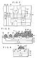
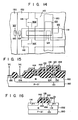
- the construction of the memory cell in the peripheral portion of the substrate will be described with reference to Figs. 2 to 4. Only one memory cell in the peripheral portion of the substrate is shown for illustrative convenience. In practice, all of a plurality of memory cells in a matrix form are formed within the p-type semiconductor region 30.
- An n-type isolation layer 42 is formed in a p-type Si substrate 40, and the p-type semiconductor region 30 is formed on the n-type isolation layer 42.
- the p-type semiconductor region 30 is surrounded by the n-type isolation layer 42 and is electrically insulated from the substrate 40.
- the plurality of DC cells 10 are formed in the p-type semiconductor region 30.
- the DC cells 10 are generally arranged in a matrix form.
- Each memory cell 10 comprises the n-type source region 14, the n-type drain region 16, the n-type data updating region 24 connected to the drain region 16, the first control gate 18, the second control gate 20, the floating gate 22, and gate oxide films 44, 46, 48 and 50.
- the source region 14, the drain region 16, and the data updating region 24 are formed in the p-type semiconductor region 30.
- the second control gate 20 is formed above the floating gate 22, and the first control gate 18 is formed on the second control gate 20.
- the gate oxide film 44 is formed between the channel region and the floating gate 22.
- the gate oxide film 46 is formed between the channel region and the first control gate 18, between the drain region 16 and the first control gate 18 and between the floating gate 22 and the first control gate 18.
- the gate oxide film 48 is formed between the second control gate 20 and the first control gate 18.
- the gate oxide film 50 is formed between the data updating region 24 and the floating gate 22.
- a potential Va is supplied to the p-type semiconductor region 30 through a p +- type diffusion layer 52.
- a potential Vb is supplied to the n-type isolation layer 42 through an n +- type diffusion layer 54.
- a potential Vc is supplied to the semiconductor substrate 40 through a p +- type diffusion layer 56.
- a potential Vs is supplied to the drain region 16 and the data updating region 24.
- the write/erase operation of the memory cell 10 is performed as follows.
- Vc 0 V
- a high potential e.g., 20 V
- Electrons are then injected from the data updating region 24 to the floating gate 22 due to the tunnel effect.
- a voltage is not applied across the p-n junctions formed between the drain region 16 and the p-type semiconductor region 30 and between the data updating region 24 and semiconductor region 30, thus preventing the surface breakdown.
- a voltage is not applied between the n-type isolation layer 42 and the p-type Si substrate 40, thus preventing the breakdown between the n-type isolation layer 42 and the p-type Si substrate 40.
- the electrons are shifted from the floating gate 22 to the data updating region 24 by the tunnel effect, thereby completing electron emission.
- no breakdown occurs since a voltage is not applied across the p-n junctions formed between the drain region 16 and the p-type semiconductor region 30 and between the data updating region 24 and the p-type semiconductor region 30, no breakdown occurs.
- an n- type layer may be inserted to constitute a p-n junction with the substrate.
- the packing density of the device will not be decreased.
- an n-type impurity such as arsenic or phosphorus may be ion-implanted in the p-type Si substrate 40 at an acceleration voltage of 200 to 1,000 kV to form the n-type isolation layer 42 and the p-type semiconductor region 30.
- an n-type layer may be formed on the p-type substrate 40 by ion implantation or diffusion, a p-type epitaxial layer may be formed thereon, and ion implantation or diffusion is performed with respect to the n-type layer, thereby forming the n-type isolation layer 42 and the p-type semiconductor region 30.
- a highly integrated EEPROM having a high dielectric strength can be obtained according to this embodiment of the present invention.
- the thickness of the oxide film of the memory cell and the junction depth can be freely selected in accordance with micropatterns of the memory cells based on the scaling rules.
- the present invention is very effective for micropatterning the memory cells. Unlike the conventional device wherein the dielectric strength is increased by a low impurity concentration diffusion layer, the fabrication process will not be complicated and the read characteristics of the memory cells will not be degraded.
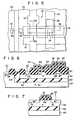
- an electrically erasable programable nonvolatile semiconductor memory device will be described with reference to Figs. 5 to 7.
- an insulating layer 60 made of silicon oxide (Si0 2 ) is formed between a p-type Si substrate 40 and a p-type common semiconductor region 30. Therefore, the p-type semiconductor region 30 is electrically insulated from the p-type Si substrate 40.
- Oxygen is ion-implanted in the p-type substrate 40 at a dose of 1 x 10"/cm 2 and at an acceleration voltage of 200 kV, and the resultant structure is annealed in a nitrogen atmosphere at a temperature of 1,000°C for about an hour, thereby forming a buried oxide layer 62.
- the p-type Si substrate 40 is then selectively oxidized to form an oxide region 64 connected to the oxide layer 62, thereby preparing the insulating layer 60.
- Any other arrangement of the second embodiment is substantially the same as that of the first embodiment.
- the same reference numerals as in the second embodiment denote the same parts as in the first embodiment, and a detailed description will be omitted.
- the write/erase operation of the memory cell will be performed as follows.
- the Si substrate 40 is set at a fixed potential Vc of 0 V.
- Vc 0 V
- the condition Va 0 V is established
- the data updating region 24 is set at a potential Vs of 0 V
- a high potential e.g., 20 V
- the electrons are then injected from the data updating region 24 to the floating gate 22 by the tunnel effect.
- a hig voltage is not applied across p-n junctions between the drain region 16 and the p-type semiconductor region 30 and between the data updating region 24 and the p-type semiconductor region 30, thereby preventing the surface breakdown effect.
- the p-type semiconductor region 30 is electrically insulated from the p-type Si substrate 40 through the insulating layer 60, no breakdown occurs.
- the electrons are shifted from the floating gate 22 to the data updating region 24 by the tunnel effect.
- no voltage is applied across p-n junctions between the drain region 16 and the p-type semiconductor region 30 and between the data updating region 24 and the p-type semiconductor region 30, thereby preventing the breakdown phenomenon.
- the p-type semiconductor region 30 and the p-type Si substrate 40 are set at 20 V and 0 V, respectively. However, since the p-type semiconductor region 30 is isolated by the insulating layer 60 from the p-type Si substrate 40, no breakdown occurs.
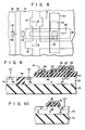
- a first semiconductor region 72 and a second semiconductor region 74 are formed on an insulating substrate 70 made of, for example, sapphire.
- the first and second semiconductor regions 72 and 74 constitute silicon islands and are isolated by an insulating region 76.
- a plurality of memory cells are formed in the first semiconductor region 72 in the same manner as the previous embodiments.
- a peripheral circuit is formed in the second semiconductor region 74.
- the cell arrangement of the third embodiment is substantially the same as those of the first and second embodiments.
- the same reference numerals as in the third embodiment denote the same parts as in first and second embodiments, and a detailed description thereof will be omitted.
- a voltage (e.g., 20 V) is applied between the floating gate 22 and the data updating region 24.
- the n-type data updating region 24 is kept at the same potential as that of the p-type first semiconductor region 72.
- the potential Vs the n-type data updating region 24 is the same as the potential Va at the first semiconductor region 72. Since no voltage is applied across the p-n junction between the data updating region 24 and the first semiconductor region 72, no surface breakdown will occur in this p-n junction.
- the potential Vc at the second semiconductor region 74 is normally 0 V.
- the first semiconductor region 72 is electrically insulated from the second semiconductor region 74 through the insulating substrate 70 and the insulating region 76, thus preventing the breakdown phenomenon. According to the third embodiment, the same effect as in the first embodiment can be obtained.
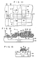
- All cells 10 are formed in a p-type well region 82 in an n-type Si substrate 80 in this embodiment.
- the p-type well region 82 is electrically insulated from the n-type Si substrate 80 through a p-n junction 81 formed between the p-type well region 82 and the n-type Si substrate 80.
- Each memory cell 10 comprises an n-type source region 14, an n-type drain region 16, an n-type data updating region 24 connected to the drain region 16, a first control gate 18, a second control gate 20, a floating gate 22, and gate oxide films 44, 46, 48 and 50.
- the source region 14, the drain region 16, and the data updating region 24 are formed in the p-type well region 82.
- the second control gate 20 is formed above the floating gate 22, and the first control gate 18 is formed above the second control gate 20.
- the gate oxide film 44 is formed between a channel region and the floating gate 22.
- the gate oxide film 46 is formed between the channel region and the first control gate 18, between the drain region 16 and the first control gate 18 and between the floating gate 22 and the first control gate 18.
- the gate oxide film 48 is formed between the second control gate 20 and the first control gate 18.
- the gate oxide film 50 is formed between the data updating region 24 and the floating gate 22.
- a potential Va is applied to the p-type well region 82 through a p +- type diffusion layer 84, and a potential Vc is applied to the semiconductor substrate 80 through an n +- type diffusion layer 86.
- a potential Vs is applied to the drain region 16 and the data updating region 24.
- a potential Vc at the n-type Si substrate 80 is a fixed potential Vdd of +5 V.
- the first and second control gates 18 and 20 are set at a voltage of -15 V, and the data updating region 24 has a potential Vs of +5 V.
- the electrons are emitted from the floating gate 22 to the data updating region 24 by the tunnel effect, so that the threshold voltage of the memory cell 10 is shifted in the negative direction.
- the potential Va at the p-type well region 82 is set to be. equal to the potential Vs at the data updating region 24.
- the surface breakdown phenomenon tends to occur in a conventional device.
- the electric field is not concentrated, thereby preventing the breakdown phenomenon.
- one of the control gates is set at a potential of +5 V, a sufficient potential difference between the floating gate 22 and the data updating region 24 will not be generated, thus disabling emission of electrons.
- the electrons are injected from the data updating region 24 to the floating gate 22.
- the first and second gates 18 and 20 are set at a potential of +5 V
- the data updating region 24 and the p-type well region 82 are respectively set at potentials Vs and Va of -15 V.
- the electrons are injected from the data updating region 24 to the floating gate by the tunnel effect, so that the threshold voltage of the memory cell is shifted in the positive direction.
- the data updating region 24 and the p-type well region 82 are kept at the same potential, and no voltage is applied across the p-n junction therebetween, thereby preventing the surface breakdown phenomenon.
- the same effect as in the first embodiment can be obtained.
- the p-type well region 82 is formed by using the n-type substrate 80 in the fourth embodiment, a negative potential can be easily generated in the chip. A signal is decoded to easily apply this negative potential to only the necessary control gate. This is because this p-type well region 82 is electrically isolated through the n-type substrate 80 from another well region which is biased to 0 V. Therefore, the p-type well region 82 is charged to generate the negative potential within the chip.
- memory cells 110 comprise p-channel memory cells. All the memory cells 110 are formed in an n-type well region 182 in a p-type Si substrate 180.
- the n-type well region 182 is electrically isolated from the p-type Si substrate 180 through a p-n junction 181 between the n-type well region 182 and the p-type Si substrate 180.
- Each memory cell 110 comprises a p-type source region 114, a p-type drain region 116, a p-type data updating region 124 connected to the drain region 116, a first control gate 118, a second control gate 120, a floating gate 122, and gate oxide films 144, 146, 148 and 150.
- the source region 114, the drain region 116, and the data updating region 124 are formed within the n-type well region 182.
- the second control gate 120 is formed above the floating gate 122, and a first control gate 118 is formed above the second control gate 120.
- the gate oxide film 144 is formed between the channel region and the floating gate 122.
- the gate oxide film 146 is formed between the channel region and the first control gate 118, between the drain region 116 and the first control gate 118 and between the floating gate 122 and the first control gate 118.
- the gate oxide film 148 is formed between the second control gate 120 and the first control gate 118.
- the gate oxide film 150 is formed between the data updating region 124 and the floating gate 122.
- a potential Va is applied to the n-type well region 182 through an n +- type diffusion layer 184, and a potential Vc is applied to the semiconductor substrate 180 through a p +- type diffusion layer 186.
- a potential Vs is applied to the drain region 116 and the data updating region 124.
- the potential Vc at the substrate is a fixed potential Vss of 0 V.
- the first and second control gates 118 and 120 are set at a potential of +20 V, and the potential Vs at the data updating region 124 is the ground potential of 0 V.
- the electrons are injected from the data updating region 24 to the floating gate 122 by the tunnel effect, so that the threshold voltage of the memory cell 110 is shifted in the positive direction.
- the potential Va at the n-type well region 182 is the same as the potential Vs at the data updating region 124.
- the thickness of the depletion layer is thin at a portion 188 located in a position where the p-n junction is in contact with the gate oxide film 146, and thus the electric field is concentrated therein. Therefore, according to the conventional device, the surface breakdown phenomenon tends to occur. However, according to the device of the present invention, since a voltage is not applied across the p-n junction, the electric field is not concentrated, thereby completely preventing the breakdown phenomenon. When one of the control gates is set at 0 V, a sufficient potential difference between the floating gate 122 and the data updating region 124 does not occur, thereby disabling the injection of the electrons.
- the first and second control gates 118 and 120 are set at 0 V, and the potential Vs at the data updating region 124 and the potential Va at the n-type well region 182 are set at a potential of 20 V.
- the electrons are emitted from the floating gate 122 to the data updating region 124 by the tunnel effect, so that the threshold voltage of the memory cell 110 is shifted in the negative direction.
- the data updating region 124 and the n-type well region 182 are kept at the same potential. As a result, no voltage is applied to the p-n junction between the regions 124 and 182, and thus the surface breakdown phenomenon is prevented.
- the p-n junction 181 between the n-type well region 182 and the p-type Si substrate 180 receives a potential of 20 V.
- the dielectric withstand voltage of the n-type well region 182 can be more than 20 V irrespective of micropattering of the memory cells. Therefore, no breakdown phenomenon will occur.
- the position of the source may be replaced with that of the drain.
- the high voltage for data write/erase operation is not limited to the value exemplified in the above embodiments.
Landscapes
- Engineering & Computer Science (AREA)
- Microelectronics & Electronic Packaging (AREA)
- Non-Volatile Memory (AREA)
- Semiconductor Memories (AREA)
Claims (12)
Applications Claiming Priority (4)
| Application Number | Priority Date | Filing Date | Title |
|---|---|---|---|
| JP179561/83 | 1983-09-28 | ||
| JP179560/83 | 1983-09-28 | ||
| JP58179561A JPS6072276A (ja) | 1983-09-28 | 1983-09-28 | 不揮発性半導体記憶装置 |
| JP58179560A JPS6072275A (ja) | 1983-09-28 | 1983-09-28 | 不揮発性半導体記憶装置 |
Publications (3)
| Publication Number | Publication Date |
|---|---|
| EP0138439A2 EP0138439A2 (de) | 1985-04-24 |
| EP0138439A3 EP0138439A3 (en) | 1987-08-26 |
| EP0138439B1 true EP0138439B1 (de) | 1990-12-19 |
Family
ID=26499367
Family Applications (1)
| Application Number | Title | Priority Date | Filing Date |
|---|---|---|---|
| EP84306502A Expired EP0138439B1 (de) | 1983-09-28 | 1984-09-24 | Elektrisch löschbare und programmierbare nichtflüchtige Halbleiterspeicheranordnung mit zwei Gate-Elektroden |
Country Status (2)
| Country | Link |
|---|---|
| EP (1) | EP0138439B1 (de) |
| DE (1) | DE3483765D1 (de) |
Families Citing this family (9)
| Publication number | Priority date | Publication date | Assignee | Title |
|---|---|---|---|---|
| US5055897A (en) * | 1988-07-27 | 1991-10-08 | Intel Corporation | Semiconductor cell for neural network and the like |
| US5196912A (en) * | 1988-10-28 | 1993-03-23 | Casio Computer Co., Ltd. | Thin film transistor having memory function and method for using thin film transistor as memory element |
| CA2001682C (en) * | 1988-10-28 | 1994-05-03 | Hiroshi Matsumoto | Thin film transistor having memory function and method for using thin film transistor as memory element |
| GB2236881B (en) * | 1989-10-11 | 1994-01-12 | Intel Corp | Improved synapse cell employing dual gate transistor structure |
| US5212541A (en) * | 1991-04-18 | 1993-05-18 | National Semiconductor Corporation | Contactless, 5v, high speed eprom/flash eprom array utilizing cells programmed using source side injection |
| US5541875A (en) * | 1994-07-01 | 1996-07-30 | Advanced Micro Devices, Inc. | High energy buried layer implant to provide a low resistance p-well in a flash EPROM array |
| KR100217901B1 (ko) * | 1996-03-11 | 1999-09-01 | 김영환 | 플래쉬 이이피롬 셀 및 그 제조방법 |
| KR100387267B1 (ko) * | 1999-12-22 | 2003-06-11 | 주식회사 하이닉스반도체 | 멀티 레벨 플래쉬 이이피롬 셀 및 그 제조 방법 |
| JP4065671B2 (ja) * | 2001-08-31 | 2008-03-26 | シャープ株式会社 | 不揮発性半導体記憶装置、その製造方法及びその動作方法 |
Family Cites Families (4)
| Publication number | Priority date | Publication date | Assignee | Title |
|---|---|---|---|---|
| DE2921993A1 (de) * | 1979-05-30 | 1980-12-04 | Siemens Ag | Halbleiterspeicher |
| US4297719A (en) * | 1979-08-10 | 1981-10-27 | Rca Corporation | Electrically programmable control gate injected floating gate solid state memory transistor and method of making same |
| JPS56162860A (en) * | 1980-05-19 | 1981-12-15 | Toshiba Corp | Semiconductor device |
| US4490900A (en) * | 1982-01-29 | 1985-01-01 | Seeq Technology, Inc. | Method of fabricating an MOS memory array having electrically-programmable and electrically-erasable storage devices incorporated therein |
-
1984
- 1984-09-24 DE DE8484306502T patent/DE3483765D1/de not_active Expired - Lifetime
- 1984-09-24 EP EP84306502A patent/EP0138439B1/de not_active Expired
Also Published As
| Publication number | Publication date |
|---|---|
| EP0138439A3 (en) | 1987-08-26 |
| EP0138439A2 (de) | 1985-04-24 |
| DE3483765D1 (de) | 1991-01-31 |
Similar Documents
| Publication | Publication Date | Title |
|---|---|---|
| KR100316086B1 (ko) | 신규한프로그래밍수단을갖는고밀도'전기적으로소거가능하고프로그램가능한판독전용메모리(eeprom)'셀어레이및이를제조하는방법 | |
| JP2555027B2 (ja) | 半導体記憶装置 | |
| US6873004B1 (en) | Virtual ground single transistor memory cell, memory array incorporating same, and method of operation thereof | |
| US4701776A (en) | MOS floating gate memory cell and process for fabricating same | |
| US6703659B2 (en) | Low voltage programmable and erasable flash EEPROM | |
| US5086325A (en) | Narrow width EEPROM with single diffusion electrode formation | |
| US4822750A (en) | MOS floating gate memory cell containing tunneling diffusion region in contact with drain and extending under edges of field oxide | |
| KR100316089B1 (ko) | 폴리터널스페이서를갖는완전특징고밀도"전기적으로소거가능하고프로그램가능한판독전용메모리(eeprom)"셀을제조하는방법 | |
| US5615152A (en) | Method of erasing a high density contactless flash EPROM array | |
| JPS637031B2 (de) | ||
| JPS6329980A (ja) | 持久記憶型半導体メモリデバイス | |
| US5340760A (en) | Method of manufacturing EEPROM memory device | |
| US6905929B1 (en) | Single poly EPROM cell having smaller size and improved data retention compatible with advanced CMOS process | |
| KR100394425B1 (ko) | 3중 웰 구조 내의 두꺼운 필드 분리 영역에 이용하기 위한 채널 스톱 방법 | |
| US6570212B1 (en) | Complementary avalanche injection EEPROM cell | |
| EP0160003B1 (de) | Mos-speicherzelle mit schwimmendem gate und verfahren zu ihrer verfertigung | |
| US6326663B1 (en) | Avalanche injection EEPROM memory cell with P-type control gate | |
| EP0138439B1 (de) | Elektrisch löschbare und programmierbare nichtflüchtige Halbleiterspeicheranordnung mit zwei Gate-Elektroden | |
| JPH10189920A (ja) | 不揮発性半導体記憶装置及びその製造方法 | |
| EP0690508B1 (de) | Speichermatrix mit einer vergrabenen Schicht und Löschverfahren | |
| US5189497A (en) | Semiconductor memory device | |
| US20020055228A1 (en) | Sidewall process to improve the flash memory cell performance | |
| US5019881A (en) | Nonvolatile semiconductor memory component | |
| US5472891A (en) | Method of manufacturing a semiconductor device | |
| KR100361391B1 (ko) | 비휘발성 반도체 디바이스 및 그 제조 방법 |
Legal Events
| Date | Code | Title | Description |
|---|---|---|---|
| PUAI | Public reference made under article 153(3) epc to a published international application that has entered the european phase |
Free format text: ORIGINAL CODE: 0009012 |
|
| 17P | Request for examination filed |
Effective date: 19841003 |
|
| AK | Designated contracting states |
Designated state(s): DE FR GB |
|
| PUAL | Search report despatched |
Free format text: ORIGINAL CODE: 0009013 |
|
| AK | Designated contracting states |
Kind code of ref document: A3 Designated state(s): DE FR GB |
|
| 17Q | First examination report despatched |
Effective date: 19900221 |
|
| GRAA | (expected) grant |
Free format text: ORIGINAL CODE: 0009210 |
|
| AK | Designated contracting states |
Kind code of ref document: B1 Designated state(s): DE FR GB |
|
| PG25 | Lapsed in a contracting state [announced via postgrant information from national office to epo] |
Ref country code: FR Effective date: 19901219 |
|
| REF | Corresponds to: |
Ref document number: 3483765 Country of ref document: DE Date of ref document: 19910131 |
|
| EN | Fr: translation not filed | ||
| PG25 | Lapsed in a contracting state [announced via postgrant information from national office to epo] |
Ref country code: GB Effective date: 19910924 |
|
| PLBE | No opposition filed within time limit |
Free format text: ORIGINAL CODE: 0009261 |
|
| STAA | Information on the status of an ep patent application or granted ep patent |
Free format text: STATUS: NO OPPOSITION FILED WITHIN TIME LIMIT |
|
| 26N | No opposition filed | ||
| GBPC | Gb: european patent ceased through non-payment of renewal fee | ||
| PGFP | Annual fee paid to national office [announced via postgrant information from national office to epo] |
Ref country code: DE Payment date: 19971010 Year of fee payment: 14 |
|
| PG25 | Lapsed in a contracting state [announced via postgrant information from national office to epo] |
Ref country code: DE Free format text: LAPSE BECAUSE OF NON-PAYMENT OF DUE FEES Effective date: 19990701 |