EP0043029A2 - Gesintertes, mehrschichtiges, keramisches Substrat und Verfahren zu seiner Herstellung - Google Patents
Gesintertes, mehrschichtiges, keramisches Substrat und Verfahren zu seiner Herstellung Download PDFInfo
- Publication number
- EP0043029A2 EP0043029A2 EP81104630A EP81104630A EP0043029A2 EP 0043029 A2 EP0043029 A2 EP 0043029A2 EP 81104630 A EP81104630 A EP 81104630A EP 81104630 A EP81104630 A EP 81104630A EP 0043029 A2 EP0043029 A2 EP 0043029A2
- Authority
- EP
- European Patent Office
- Prior art keywords
- vias
- center
- sheets
- substrate
- pattern
- Prior art date
- Legal status (The legal status is an assumption and is not a legal conclusion. Google has not performed a legal analysis and makes no representation as to the accuracy of the status listed.)
- Granted
Links
Images
Classifications
-
- H—ELECTRICITY
- H10—SEMICONDUCTOR DEVICES; ELECTRIC SOLID-STATE DEVICES NOT OTHERWISE PROVIDED FOR
- H10W—GENERIC PACKAGES, INTERCONNECTIONS, CONNECTORS OR OTHER CONSTRUCTIONAL DETAILS OF DEVICES COVERED BY CLASS H10
- H10W70/00—Package substrates; Interposers; Redistribution layers [RDL]
- H10W70/60—Insulating or insulated package substrates; Interposers; Redistribution layers
- H10W70/67—Insulating or insulated package substrates; Interposers; Redistribution layers characterised by their insulating layers or insulating parts
- H10W70/69—Insulating materials thereof
- H10W70/692—Ceramics or glasses
-
- H—ELECTRICITY
- H10—SEMICONDUCTOR DEVICES; ELECTRIC SOLID-STATE DEVICES NOT OTHERWISE PROVIDED FOR
- H10W—GENERIC PACKAGES, INTERCONNECTIONS, CONNECTORS OR OTHER CONSTRUCTIONAL DETAILS OF DEVICES COVERED BY CLASS H10
- H10W70/00—Package substrates; Interposers; Redistribution layers [RDL]
- H10W70/01—Manufacture or treatment
- H10W70/05—Manufacture or treatment of insulating or insulated package substrates, or of interposers, or of redistribution layers
- H10W70/095—Manufacture or treatment of insulating or insulated package substrates, or of interposers, or of redistribution layers of vias therein
-
- H—ELECTRICITY
- H10—SEMICONDUCTOR DEVICES; ELECTRIC SOLID-STATE DEVICES NOT OTHERWISE PROVIDED FOR
- H10W—GENERIC PACKAGES, INTERCONNECTIONS, CONNECTORS OR OTHER CONSTRUCTIONAL DETAILS OF DEVICES COVERED BY CLASS H10
- H10W70/00—Package substrates; Interposers; Redistribution layers [RDL]
- H10W70/60—Insulating or insulated package substrates; Interposers; Redistribution layers
- H10W70/611—Insulating or insulated package substrates; Interposers; Redistribution layers for connecting multiple chips together
-
- H—ELECTRICITY
- H10—SEMICONDUCTOR DEVICES; ELECTRIC SOLID-STATE DEVICES NOT OTHERWISE PROVIDED FOR
- H10W—GENERIC PACKAGES, INTERCONNECTIONS, CONNECTORS OR OTHER CONSTRUCTIONAL DETAILS OF DEVICES COVERED BY CLASS H10
- H10W70/00—Package substrates; Interposers; Redistribution layers [RDL]
- H10W70/60—Insulating or insulated package substrates; Interposers; Redistribution layers
- H10W70/67—Insulating or insulated package substrates; Interposers; Redistribution layers characterised by their insulating layers or insulating parts
- H10W70/68—Shapes or dispositions thereof
- H10W70/685—Shapes or dispositions thereof comprising multiple insulating layers
-
- H—ELECTRICITY
- H05—ELECTRIC TECHNIQUES NOT OTHERWISE PROVIDED FOR
- H05K—PRINTED CIRCUITS; CASINGS OR CONSTRUCTIONAL DETAILS OF ELECTRIC APPARATUS; MANUFACTURE OF ASSEMBLAGES OF ELECTRICAL COMPONENTS
- H05K1/00—Printed circuits
- H05K1/02—Details
- H05K1/0271—Arrangements for reducing stress or warp in rigid printed circuit boards, e.g. caused by loads, vibrations or differences in thermal expansion
-
- H—ELECTRICITY
- H05—ELECTRIC TECHNIQUES NOT OTHERWISE PROVIDED FOR
- H05K—PRINTED CIRCUITS; CASINGS OR CONSTRUCTIONAL DETAILS OF ELECTRIC APPARATUS; MANUFACTURE OF ASSEMBLAGES OF ELECTRICAL COMPONENTS
- H05K1/00—Printed circuits
- H05K1/02—Details
- H05K1/0296—Conductive pattern lay-out details not covered by sub groups H05K1/02 - H05K1/0295
- H05K1/0298—Multilayer circuits
-
- H—ELECTRICITY
- H05—ELECTRIC TECHNIQUES NOT OTHERWISE PROVIDED FOR
- H05K—PRINTED CIRCUITS; CASINGS OR CONSTRUCTIONAL DETAILS OF ELECTRIC APPARATUS; MANUFACTURE OF ASSEMBLAGES OF ELECTRICAL COMPONENTS
- H05K1/00—Printed circuits
- H05K1/02—Details
- H05K1/03—Use of materials for the substrate
- H05K1/0306—Inorganic insulating substrates, e.g. ceramic, glass
-
- H—ELECTRICITY
- H05—ELECTRIC TECHNIQUES NOT OTHERWISE PROVIDED FOR
- H05K—PRINTED CIRCUITS; CASINGS OR CONSTRUCTIONAL DETAILS OF ELECTRIC APPARATUS; MANUFACTURE OF ASSEMBLAGES OF ELECTRICAL COMPONENTS
- H05K3/00—Apparatus or processes for manufacturing printed circuits
- H05K3/46—Manufacturing multilayer circuits
- H05K3/4611—Manufacturing multilayer circuits by laminating two or more circuit boards
- H05K3/4626—Manufacturing multilayer circuits by laminating two or more circuit boards characterised by the insulating layers or materials
- H05K3/4629—Manufacturing multilayer circuits by laminating two or more circuit boards characterised by the insulating layers or materials laminating inorganic sheets comprising printed circuits, e.g. green ceramic sheets
-
- H—ELECTRICITY
- H05—ELECTRIC TECHNIQUES NOT OTHERWISE PROVIDED FOR
- H05K—PRINTED CIRCUITS; CASINGS OR CONSTRUCTIONAL DETAILS OF ELECTRIC APPARATUS; MANUFACTURE OF ASSEMBLAGES OF ELECTRICAL COMPONENTS
- H05K3/00—Apparatus or processes for manufacturing printed circuits
- H05K3/46—Manufacturing multilayer circuits
- H05K3/4644—Manufacturing multilayer circuits by building the multilayer layer by layer, i.e. build-up multilayer circuits
- H05K3/4673—Application methods or materials of intermediate insulating layers not specially adapted to any one of the previous methods of adding a circuit layer
- H05K3/4676—Single layer compositions
-
- H—ELECTRICITY
- H10—SEMICONDUCTOR DEVICES; ELECTRIC SOLID-STATE DEVICES NOT OTHERWISE PROVIDED FOR
- H10W—GENERIC PACKAGES, INTERCONNECTIONS, CONNECTORS OR OTHER CONSTRUCTIONAL DETAILS OF DEVICES COVERED BY CLASS H10
- H10W70/00—Package substrates; Interposers; Redistribution layers [RDL]
- H10W70/60—Insulating or insulated package substrates; Interposers; Redistribution layers
- H10W70/62—Insulating or insulated package substrates; Interposers; Redistribution layers characterised by their interconnections
- H10W70/63—Vias, e.g. via plugs
-
- H—ELECTRICITY
- H10—SEMICONDUCTOR DEVICES; ELECTRIC SOLID-STATE DEVICES NOT OTHERWISE PROVIDED FOR
- H10W—GENERIC PACKAGES, INTERCONNECTIONS, CONNECTORS OR OTHER CONSTRUCTIONAL DETAILS OF DEVICES COVERED BY CLASS H10
- H10W72/00—Interconnections or connectors in packages
- H10W72/071—Connecting or disconnecting
- H10W72/072—Connecting or disconnecting of bump connectors
- H10W72/07251—Connecting or disconnecting of bump connectors characterised by changes in properties of the bump connectors during connecting
-
- H—ELECTRICITY
- H10—SEMICONDUCTOR DEVICES; ELECTRIC SOLID-STATE DEVICES NOT OTHERWISE PROVIDED FOR
- H10W—GENERIC PACKAGES, INTERCONNECTIONS, CONNECTORS OR OTHER CONSTRUCTIONAL DETAILS OF DEVICES COVERED BY CLASS H10
- H10W72/00—Interconnections or connectors in packages
- H10W72/20—Bump connectors, e.g. solder bumps or copper pillars; Dummy bumps; Thermal bumps
-
- H—ELECTRICITY
- H10—SEMICONDUCTOR DEVICES; ELECTRIC SOLID-STATE DEVICES NOT OTHERWISE PROVIDED FOR
- H10W—GENERIC PACKAGES, INTERCONNECTIONS, CONNECTORS OR OTHER CONSTRUCTIONAL DETAILS OF DEVICES COVERED BY CLASS H10
- H10W90/00—Package configurations
- H10W90/701—Package configurations characterised by the relative positions of pads or connectors relative to package parts
- H10W90/721—Package configurations characterised by the relative positions of pads or connectors relative to package parts of bump connectors
- H10W90/724—Package configurations characterised by the relative positions of pads or connectors relative to package parts of bump connectors between a chip and a stacked insulating package substrate, interposer or RDL
Definitions
- the invention relates to a sintered multi-layer ceramic (MLC) substrate formed of a plurality of ceramic green sheets that are provided with metallurgy patterns and/or metal filled vias f laminated together and sintered, and to a method of fabricating especially such a sintered MLC substrate, wherein a plurality of ceramic green sheets are formed and provided with vias, wherein using a conductive metallurgy paste a metallurgy pattern is printed on the green sheets and the vias are filled and wherein the sheets are stacked, laminated together and sintered.
- MLC sintered multi-layer ceramic
- Ceramic materials find wide and diverse use in the fabrication of various types of elements and articles. Ceramic materials have found use in the fabrication of electrical components such as capacitors, and semiconductor device packages for supporting semiconductor devices. Such packages are comprised of a ceramic substrate with printed conductive metallurgy stripes connected to the device and to I/O pins or other connections which are joined to boards or the like. While many techniques are known for forming ceramic substrates for use in fabricating electrical components, one of the most popular procedures for such fabrication involves the casting of what is termed a "ceramic green sheet" and the subsequent processing and firing of the ceramic green sheet. Laminated multi-layer ceramic substrates provided with internal wiring are well known as illustrated and described in U.S. 3,564,114.
- Multi-layer ceramic substrates capable of mounting and interconnecting a plurality of semiconductor devices are well known and are described by an article entitled "A Fabrication Technique for Multi-Layer Ceramic Modules" by H. D. Kaiser et al in Solid State Technology, May 1972 P. 35 - 40.
- a sophisticated embodiment of a semiconductor package which embodies a multi-layer ceramic substrate is claimed and described in US 4 245 273.
- green sheets of ceramic i.e., ceramic powder held togther in sheet form by a temporary organic binder, are punched to form via holes, the via holes subsequently filled with a conductive paste, and metallurgy lines also formed on the surface, usually by screen printing.
- the conductive paste is formed of a refractory metal which will withstand the subsequent sintering process.
- the metallized sheets are stacked, laminated, and fired to form a monolithic multi-layer substrate with a complex internal electrical circuitry.
- This substrate structure is particularly advantageous since it affords an opportunity to do three-dimensional wiring in the substrate in what was normally waste or inaccessible space. The use of this waste space results in the creation of a high density sturdy electronic package with good performance and reliability.
- the fabrication of a multi- layer cercmic substrate though simple in principal, is highly complex since the high temperature sintering process may cause reactions to occur between the components of the metallurgy and ceramic, and generate internal stresses which can cause de-lamination and cracking. As the substrate is cooled down from the sintering temperature, internal stresses are generated which can cause cracking and warpage if they are severe. This is due to different coefficients of expansion of the ceramic and conductive metal.
- a desirable technique for mounting semiconductor devices on a multi-layer ceramic substrate is solder bonding the device to the substrate.
- many solder pads on the surface of the device are joined to a similar pattern of pads on the substrate.
- This requires a large number of closely-spaced via holes filled with conductive metal in the top layer of the substrate.
- a problem experienced in fabricating such a substrate is the formation of via-to-via cracks. These cracks are basically the result of thermal expansion mis-match between the conductive metal in the vias, and the ceramic material. Avoiding this thermal expansion mis-match is difficult because of the limited selection of conductive metals which will withstand the sintering temperature and also ceramic materials that will satisfy the demands of packaging.
- the object of the invention is to provide a multi-layer printed semiconductor package or more particularly a fired multi-layer ceramic (MLC) substrate adapted to interconnect a plurality of large scale integrated circuit chips mounted on the substrate and being not or only slightly susceptible to cracking, and a process to produce such a substrate.
- MLC multi-layer ceramic
- the fired multi-layer ceramic substrate according to the invention is less susceptible to cracking, as well as stronger and more reliable than the MLC substrate of the prior art.
- the inventive substrate is free or substantially free of cracks between closely spaced, metal - filled vias in the top layer.
- the pattern of closely spaced vias in the top layer of the MLC substrate corresponds,to the I/O pads of LSI circuit chips mounted on the substrate. There is no cracking even if the difference of the coefficients of expansion of the sintered ceramic material and the sintered metallurgy paste is in the order of .8 x 10 /°C.
- the suprisingly low susceptibility of the inventive MLC substrate is due to the thickness ratio between the top sheet and the underlying sheets used to form the MLC substrate.
- the method for producing the multi-layer substrate according to the inventioh can be practised without significantly departing from the known fabrication technique.
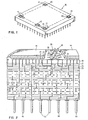
- Fig. 1 of the drawings there is illustrated a typical laminated multi-layer ceramic substrate in which the concept of our invention can be applied.
- the substrate 10 can be of any suitable size to accommodate the desired number of devices.
- the devices on the substrate can be of the order of 100 or more.
- -In Fig. 1 all of the device sites for joining devices to the surface are not shown in the interest of reducing drawing complexity.
- device sites would be arranged in columns and rows with typically 10 columns arranged in 10 rows, making a total of 100 devices.
- Representative sites are shown in Fig. 1.
- Substrate 10 has an internal circuitry, as described in the background section of this specification, i.e., made up of a plurality of laminated and sintered layers with via holes and printed circuits.
- FIG. 2 A cross-section of the internal circuitry is depicted in Fig. 2.
- the material of the substrate 10 is chosen for good mechanical, electrical and thermal properties so that the thermal expansion is a reasonably close match to the silicon material of the devicesto be mounted on the substrate.
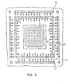
- the top surface of substrate 10 is provided with a plurality of pads 12, more clearly shown in Fig. 3, adapted to be joined to a corresponding pattern of solder pads on a semiconductor device 14.
- An asymmetrical pattern permits joining the device 14 in only one correct position, as illustrated in Fig. 3.
- Surrounding each of the cluster of pads 12 are one or more rows of engineering change pads 24. As more clearly illustrated in Fig. 2, the rows of engineering change pads 24 provide easy access to terminals 22 of device 14.
- Each of the signal input-output terminals of device 14 may be provided with an engineering change pad.
- a typical engineering change pad has a pad portion 24 and a-severable link portion 26.
- the pad portion 24 is joined to the device terminal 22 with a conductive metallurgy pattern 28.
- Pattern 28 consists of a vertically extending via 30 which extends through one or more via holes in one or more ceramic layers, a stripe portion 32 imprinted on the surface of the green sheet, and another vertical via 34 also consisting of filled via holes in one or more sheets of ceramic.
- layers 21, 23 and 25 are re-distribution layers in the substrate which perform the function of spreading out the very closely spaced pad terminals 22 of the device 14.
- the geometry of the vias and lines is larger and corresponds more to the spacing of the I/O pins 80 on the bottom surface of substrate 10.
- Internal defects such as opens or shorts in conductive lines within the substrate 10 can be corrected by connecting a wire 38 to an engineering change pad 24, as shown in Fig. 2, which thus establishes electrical contact to the associated terminal 22 of device 14.
- the associated deletable link 26 can be broken and the other end of wire 38 joined to another device terminal in similar fashion.
- two separate device terminals on different devices can be electrically connected in the event that the internal circuitry in the substrate is defective.
- the spacing of the pads in pad configuration 12 is governed by the pad configuration on the device 14 to be joined.
- Each of the pads is located over a via hole filled with conductive material which passes through the top or uppermost sheet 40 of substrate 10.
- Conductive lines joined to vias in layers 21, 23 and 25, establish electrical connections between the pads 12 and pads 24 on sheet 40.
- the top sheet 40 of substrate 10 has a via hole pattern consisting of very closely spaced vias, particularly under pads 12.
- associated with deletable links 26 there are vias filled with conductive material also contained in sheet 40.
- Conductive metals can become deposited in the cracks from plating solutions and the like used to complete the top surface metallurgy of the substrate. This can cause shorting between the pads. Still further, cracks can develop between a whole row of vias and propagate downwardly into the substrate 10. This weakens the substrate and potentially could sever the conductive lines within the substrate 10, and weaken the structure of the substrate.
- the via diameter is governed largely by the size of the punch necessary to form the vias.
- the via holes must be sufficiently small to accommodate the via patterns of the device pad configuration. However, if the vias are made very small, it will necessitate very small punch elements which are weak and wear out rapidly. Also, via holes that are smaller are more difficult to fill with conductive paste.
- the thickness of the green sheet (unfired) used to fabricate substrate 10 are in the range of 152 to 229 um. The sheets must be sufficiently thick so that they will withstand the necessary handling during processing and provide suitable electrical characteristics.
- via to via cracking can be minimized or eliminated by fabricating a multilayer ceramic substrate with the upper or outer sheet with a thickness greater than the thicknesses of the underlying green sheets. This is unexpected since in theory the incidence of via-to-via cracking should be independent of the thickness of the green sheet. Preferably in the practice of our invention, the thickness of the outer sheet should exceed the thickness of the underlying sheets by at least 20%.
- the relative sheet thicknesses is applicable in general to the several sheets directly below the upper sheet which are generally part of the fan-out metallurgy. Via to via cracking is not considered a problem except in the outer sheet.
- the vias are normally closely spaced in the upper or outer sheet, and/or possibly the underside of the substrate.
- the vias in the sheets in the center of the substrate are more widely spaced and, therefore, internal stresses sufficient to cause : , cracking are not generated. Further, the internal laminated sheets derive strength from the adjacent sheets positioned on each side which is usually sufficient to withstand any internal stresses. In contrast, the upper or outermost sheet is not as resistant to cracking since it is supported on only one side.
- the invention is applicable, therefore, when the outermost sheet contains a plurality of closely spaced vias, as in a pad cluster for solder bonding devices, and/or where there is one or more rows of closely spaced vias.
- the spacing where cracking may occur in conventional substrates is dependent on the ceramic materials, the conductive material in the vias, and the size of the vias. In general the most important factor is the difference between the difference in the coefficients of expansion of the ceramic and conductive metal.
- a differential coefficient of expansion of .8 x 10 -6 /°C, of ceramic and metal with a center to center via spacing of 175to 254 pm, and with the via diameter in the range of 35 - 55% of the center to center spacing is present in a multilayer ceramic module.
- the resultant green tape was cut into small sheets, via holes punched into the sheets, and a conductive metal paste screened into the via holes and onto the surface to form patterns.
- the sheets were assembled to form multilayered ceramic substrates.
- a conductive paste consisted of a mixture of 85% molybdenum particles, by weight, with 4% of the above-described being composed of the solid phase in the ceramic, and 15% 2,2,4 trimethylpentanideol, 1,3, mono- isobutyral, sold under the trademark "Texanol” by Eastman Kodak.
- Multi-layer ceramic substrates were formed by assembling 22 of the aforedescribed sheets, but which lacked only top sheets.
- a green ceramic sheet was doctor bladed to a dried thickness of 279 pm for the top layer of a first set of substrates that embody the method and structure of the invention.
- Conventional 203 pm sheets were placed on a second set of substrates to serve as a standard for comparison and represent the standard practice in the art.
- Identical specific via patterns were punched in both sets of top sheets in the 203 and 279 pm sheets.
- the patterns in each sheet included 9 grids of an 11 by 11 matrix of via holes where the center to center spacing was 249 pm.
- 36 individual rows of 26 vias with a center to center spacing of 249 pm were also punched. These rows were spaced from each other by a distance significantly greater than the center to center spacing.
- the diameter of all of the vias was 140 ⁇ m.
- the top sheets were assembled with the substrates consisting of the 22 previously described sheets and the resultant substrate laminated at 224 kg/cm 2 at 75°C and thereafter subjected to a sintering cycle.
- the substrates were sintered for 34 hours during which a peak temperature of 1560°C is achieved. During the sintering the substrates shrank approximately 17%.
- a comparison of the material properties of the sintered ceramic in conductive paste in the via holes is as follows:
- the coefficient of expansion indicates that internal stresses will be generated in the punched ceramic sheets which, under normal conditions, will result in cracks between vias.
- 12 substrates with an 11 mil top layer and 6 substrates with an 8 mil top layer were processed and inspected.
- the substrates were exposed to an accelerated aging environment, i.e., exposure to a plating bath.
- the plating bath was a conventional gold immersion bath at room temperature. This bath was discovered to cause a breakdown in the ceramic which permitted, after a period of time, the internal stresses to form cracks between the vias.
- the acceleration factor was one hour in the bath was equal to 3,000 hours of operation at 30°C/80% RH. Periodic inspections revealed the following via to via cracks:
- the substrates with the thicker top layer were significantly more resistant to via to via cracking.
Landscapes
- Production Of Multi-Layered Print Wiring Board (AREA)
Applications Claiming Priority (2)
| Application Number | Priority Date | Filing Date | Title |
|---|---|---|---|
| US164645 | 1980-06-30 | ||
| US06/164,645 US4302625A (en) | 1980-06-30 | 1980-06-30 | Multi-layer ceramic substrate |
Publications (3)
| Publication Number | Publication Date |
|---|---|
| EP0043029A2 true EP0043029A2 (de) | 1982-01-06 |
| EP0043029A3 EP0043029A3 (en) | 1982-09-29 |
| EP0043029B1 EP0043029B1 (de) | 1986-01-15 |
Family
ID=22595431
Family Applications (1)
| Application Number | Title | Priority Date | Filing Date |
|---|---|---|---|
| EP81104630A Expired EP0043029B1 (de) | 1980-06-30 | 1981-06-16 | Gesintertes, mehrschichtiges, keramisches Substrat und Verfahren zu seiner Herstellung |
Country Status (4)
| Country | Link |
|---|---|
| US (1) | US4302625A (de) |
| EP (1) | EP0043029B1 (de) |
| JP (1) | JPS5827665B2 (de) |
| DE (1) | DE3173490D1 (de) |
Cited By (10)
| Publication number | Priority date | Publication date | Assignee | Title |
|---|---|---|---|---|
| EP0176245A3 (en) * | 1984-08-28 | 1987-03-11 | Nec Corporation | Multilayer wiring substrate |
| EP0204261A3 (de) * | 1985-06-03 | 1987-08-12 | Hitachi, Ltd. | Mehrschichtverbindungsplatte und Verfahren zu deren Herstellung |
| EP0199635A3 (en) * | 1985-04-13 | 1987-11-19 | Fujitsu Limited | Integrated circuit device having stacked conductive layers connecting circuit elements therethrough |
| DE3630066C1 (de) * | 1986-09-04 | 1988-02-04 | Heraeus Gmbh W C | Verfahren zur Herstellung von gesinterten metallisierten Aluminiumnitrid-Keramikkoerpern |
| EP0272046A3 (de) * | 1986-12-18 | 1988-09-28 | Marconi Electronic Devices Limited | Schaltungsstruktur mit einem gemischten keramischen Substrat |
| GB2209867A (en) * | 1987-09-16 | 1989-05-24 | Advanced Semiconductor Package | Integrated circuit chip carrier |
| GB2225670A (en) * | 1988-11-30 | 1990-06-06 | Hitachi Ltd | Carrier substrate for electrical circuit element |
| EP0329133A3 (de) * | 1988-02-19 | 1990-07-11 | Microelectronics and Computer Technology Corporation | Umgekipptes Chip-Substrat |
| GB2229572A (en) * | 1989-03-14 | 1990-09-26 | Oxley Dev Co Ltd | Ceramic multilayer structure |
| WO1991017568A1 (en) * | 1990-04-27 | 1991-11-14 | International Business Machines Corporation | A multi-layer package incorporating a recessed cavity for a semiconductor chip |
Families Citing this family (20)
| Publication number | Priority date | Publication date | Assignee | Title |
|---|---|---|---|---|
| US4407007A (en) * | 1981-05-28 | 1983-09-27 | International Business Machines Corporation | Process and structure for minimizing delamination in the fabrication of multi-layer ceramic substrate |
| US4489364A (en) * | 1981-12-31 | 1984-12-18 | International Business Machines Corporation | Chip carrier with embedded engineering change lines with severable periodically spaced bridging connectors on the chip supporting surface |
| US4632294A (en) * | 1984-12-20 | 1986-12-30 | International Business Machines Corporation | Process and apparatus for individual pin repair in a dense array of connector pins of an electronic packaging structure |
| JPS62136098A (ja) * | 1985-12-09 | 1987-06-19 | 富士通株式会社 | 高密度配線基板 |
| WO1988005959A1 (en) * | 1987-02-04 | 1988-08-11 | Coors Porcelain Company | Ceramic substrate with conductively-filled vias and method for producing |
| US4782193A (en) * | 1987-09-25 | 1988-11-01 | Ibm Corp. | Polygonal wiring for improved package performance |
| US4882651A (en) * | 1988-12-05 | 1989-11-21 | Sprague Electric Company | Monolithic compound-ceramic capacitor |
| JP2753887B2 (ja) * | 1989-09-29 | 1998-05-20 | 京セラ株式会社 | コンデンサー内蔵複合回路基板 |
| US5302219A (en) * | 1991-04-03 | 1994-04-12 | Coors Electronic Package Company | Method for obtaining via patterns in ceramic sheets |
| US6038134A (en) * | 1996-08-26 | 2000-03-14 | Johanson Dielectrics, Inc. | Modular capacitor/inductor structure |
| US5855995A (en) * | 1997-02-21 | 1999-01-05 | Medtronic, Inc. | Ceramic substrate for implantable medical devices |
| US6231707B1 (en) | 1998-09-22 | 2001-05-15 | International Business Machines Corporation | Method of forming a multilayer ceramic substrate with max-punched vias |
| US6341417B1 (en) | 1999-09-23 | 2002-01-29 | International Business Machines Corporation | Pre-patterned substrate layers for being personalized as needed |
| US6569278B1 (en) | 1999-09-29 | 2003-05-27 | International Business Machines Corporation | Powder metal polymer organic sheet punching for substrate conductors |
| DE10250887B3 (de) * | 2002-10-31 | 2004-07-15 | Advanced Micro Devices, Inc., Sunnyvale | Schaltende Metallleitungskonfigurationen in Metallschichtstrukturen |
| US8410371B2 (en) * | 2009-09-08 | 2013-04-02 | Cree, Inc. | Electronic device submounts with thermally conductive vias and light emitting devices including the same |
| US8772817B2 (en) | 2010-12-22 | 2014-07-08 | Cree, Inc. | Electronic device submounts including substrates with thermally conductive vias |
| US8659144B1 (en) | 2011-12-15 | 2014-02-25 | Marvell International Ltd. | Power and ground planes in package substrate |
| US11489038B2 (en) | 2017-08-29 | 2022-11-01 | Micron Technology, Inc. | Capacitors having vertical contacts extending through conductive tiers |
| JP2022505218A (ja) * | 2018-10-19 | 2022-01-14 | コーニング インコーポレイテッド | ビアを備えたデバイス並びにビアを製造するための方法および材料 |
Family Cites Families (10)
| Publication number | Priority date | Publication date | Assignee | Title |
|---|---|---|---|---|
| US3726002A (en) * | 1971-08-27 | 1973-04-10 | Ibm | Process for forming a multi-layer glass-metal module adaptable for integral mounting to a dissimilar refractory substrate |
| JPS4876059A (de) * | 1972-01-14 | 1973-10-13 | ||
| GB1485569A (en) * | 1974-09-10 | 1977-09-14 | Siemens Ag | Multi-layer wired substrates for multi-chip circuits |
| US3999004A (en) * | 1974-09-27 | 1976-12-21 | International Business Machines Corporation | Multilayer ceramic substrate structure |
| US4109377A (en) * | 1976-02-03 | 1978-08-29 | International Business Machines Corporation | Method for preparing a multilayer ceramic |
| FR2350697A1 (fr) * | 1976-05-06 | 1977-12-02 | Cii | Structure perfectionnee de circuits multicouches |
| US4145273A (en) * | 1977-06-29 | 1979-03-20 | Texaco Inc. | Transformer oil processing |
| US4202007A (en) * | 1978-06-23 | 1980-05-06 | International Business Machines Corporation | Multi-layer dielectric planar structure having an internal conductor pattern characterized with opposite terminations disposed at a common edge surface of the layers |
| US4245273A (en) * | 1979-06-29 | 1981-01-13 | International Business Machines Corporation | Package for mounting and interconnecting a plurality of large scale integrated semiconductor devices |
| US4288841A (en) * | 1979-09-20 | 1981-09-08 | Bell Telephone Laboratories, Incorporated | Double cavity semiconductor chip carrier |
-
1980
- 1980-06-30 US US06/164,645 patent/US4302625A/en not_active Expired - Lifetime
-
1981
- 1981-05-20 JP JP56075056A patent/JPS5827665B2/ja not_active Expired
- 1981-06-16 DE DE8181104630T patent/DE3173490D1/de not_active Expired
- 1981-06-16 EP EP81104630A patent/EP0043029B1/de not_active Expired
Cited By (14)
| Publication number | Priority date | Publication date | Assignee | Title |
|---|---|---|---|---|
| EP0176245A3 (en) * | 1984-08-28 | 1987-03-11 | Nec Corporation | Multilayer wiring substrate |
| EP0199635A3 (en) * | 1985-04-13 | 1987-11-19 | Fujitsu Limited | Integrated circuit device having stacked conductive layers connecting circuit elements therethrough |
| EP0204261A3 (de) * | 1985-06-03 | 1987-08-12 | Hitachi, Ltd. | Mehrschichtverbindungsplatte und Verfahren zu deren Herstellung |
| DE3630066C1 (de) * | 1986-09-04 | 1988-02-04 | Heraeus Gmbh W C | Verfahren zur Herstellung von gesinterten metallisierten Aluminiumnitrid-Keramikkoerpern |
| US4818626A (en) * | 1986-09-04 | 1989-04-04 | W. C. Heraeus Gmbh | Method for producing sintered metalized aluminum nitride ceramic bodies |
| EP0272046A3 (de) * | 1986-12-18 | 1988-09-28 | Marconi Electronic Devices Limited | Schaltungsstruktur mit einem gemischten keramischen Substrat |
| GB2209867A (en) * | 1987-09-16 | 1989-05-24 | Advanced Semiconductor Package | Integrated circuit chip carrier |
| GB2209867B (en) * | 1987-09-16 | 1990-12-19 | Advanced Semiconductor Package | Method of forming an integrated circuit chip carrier |
| EP0329133A3 (de) * | 1988-02-19 | 1990-07-11 | Microelectronics and Computer Technology Corporation | Umgekipptes Chip-Substrat |
| GB2225670A (en) * | 1988-11-30 | 1990-06-06 | Hitachi Ltd | Carrier substrate for electrical circuit element |
| GB2225670B (en) * | 1988-11-30 | 1992-08-19 | Hitachi Ltd | Carrier substrate and method for preparing the same |
| GB2229572A (en) * | 1989-03-14 | 1990-09-26 | Oxley Dev Co Ltd | Ceramic multilayer structure |
| WO1991017568A1 (en) * | 1990-04-27 | 1991-11-14 | International Business Machines Corporation | A multi-layer package incorporating a recessed cavity for a semiconductor chip |
| US5081563A (en) * | 1990-04-27 | 1992-01-14 | International Business Machines Corporation | Multi-layer package incorporating a recessed cavity for a semiconductor chip |
Also Published As
| Publication number | Publication date |
|---|---|
| US4302625A (en) | 1981-11-24 |
| JPS5718350A (en) | 1982-01-30 |
| JPS5827665B2 (ja) | 1983-06-10 |
| EP0043029A3 (en) | 1982-09-29 |
| DE3173490D1 (en) | 1986-02-27 |
| EP0043029B1 (de) | 1986-01-15 |
Similar Documents
| Publication | Publication Date | Title |
|---|---|---|
| EP0043029B1 (de) | Gesintertes, mehrschichtiges, keramisches Substrat und Verfahren zu seiner Herstellung | |
| US4753694A (en) | Process for forming multilayered ceramic substrate having solid metal conductors | |
| CA1123116A (en) | Multi-layered glass-ceramic substrate for mounting of semiconductor device | |
| US5396034A (en) | Thin film ceramic multilayer wiring hybrid board | |
| US4645552A (en) | Process for fabricating dimensionally stable interconnect boards | |
| US4879156A (en) | Multilayered ceramic substrate having solid non-porous metal conductors | |
| KR100307078B1 (ko) | 기판을지지하는세라믹회로보드용글라스결합층 | |
| US4446477A (en) | Multichip thin film module | |
| US3968193A (en) | Firing process for forming a multilayer glass-metal module | |
| US5768108A (en) | Multi-layer wiring structure | |
| US4665468A (en) | Module having a ceramic multi-layer substrate and a multi-layer circuit thereupon, and process for manufacturing the same | |
| EP0609861B1 (de) | Keramisches Substrat und Verfahren zu dessen Herstellung | |
| US20080093117A1 (en) | Multilayer circuit board and manufacturing method thereof | |
| US5755903A (en) | Method of making a multilayer ceramic substrate having reduced stress | |
| US4336088A (en) | Method of fabricating an improved multi-layer ceramic substrate | |
| EP0997941B1 (de) | Leitpaste und Keramikschaltungsplatte | |
| GB2225670A (en) | Carrier substrate for electrical circuit element | |
| US6217990B1 (en) | Multilayer circuit board having no local warp on mounting surface thereof | |
| US6117367A (en) | Pastes for improved substrate dimensional control | |
| KR100748238B1 (ko) | 무수축 세라믹 기판 및 그 제조방법 | |
| JPH0817965A (ja) | 電子コンポーネントおよびその製造方法 | |
| JPH067578B2 (ja) | セラミツク多層基板 | |
| KR102952839B1 (ko) | 세라믹 그린 시트, 이의 제조 방법 및 이를 이용한 다층 세라믹 기판의 제조 방법 | |
| JPH0645758A (ja) | 多層セラミック基板およびその製造方法 | |
| JPH025027B2 (de) |
Legal Events
| Date | Code | Title | Description |
|---|---|---|---|
| PUAI | Public reference made under article 153(3) epc to a published international application that has entered the european phase |
Free format text: ORIGINAL CODE: 0009012 |
|
| AK | Designated contracting states |
Designated state(s): DE FR GB |
|
| PUAL | Search report despatched |
Free format text: ORIGINAL CODE: 0009013 |
|
| AK | Designated contracting states |
Designated state(s): DE FR GB |
|
| 17P | Request for examination filed |
Effective date: 19830208 |
|
| GRAA | (expected) grant |
Free format text: ORIGINAL CODE: 0009210 |
|
| AK | Designated contracting states |
Designated state(s): DE FR GB |
|
| ET | Fr: translation filed | ||
| REF | Corresponds to: |
Ref document number: 3173490 Country of ref document: DE Date of ref document: 19860227 |
|
| PLBE | No opposition filed within time limit |
Free format text: ORIGINAL CODE: 0009261 |
|
| STAA | Information on the status of an ep patent application or granted ep patent |
Free format text: STATUS: NO OPPOSITION FILED WITHIN TIME LIMIT |
|
| 26N | No opposition filed | ||
| PGFP | Annual fee paid to national office [announced via postgrant information from national office to epo] |
Ref country code: GB Payment date: 19910528 Year of fee payment: 11 |
|
| PGFP | Annual fee paid to national office [announced via postgrant information from national office to epo] |
Ref country code: DE Payment date: 19910619 Year of fee payment: 11 |
|
| PGFP | Annual fee paid to national office [announced via postgrant information from national office to epo] |
Ref country code: FR Payment date: 19920601 Year of fee payment: 12 |
|
| PG25 | Lapsed in a contracting state [announced via postgrant information from national office to epo] |
Ref country code: GB Effective date: 19920616 |
|
| GBPC | Gb: european patent ceased through non-payment of renewal fee |
Effective date: 19920616 |
|
| PG25 | Lapsed in a contracting state [announced via postgrant information from national office to epo] |
Ref country code: DE Effective date: 19930302 |
|
| PG25 | Lapsed in a contracting state [announced via postgrant information from national office to epo] |
Ref country code: FR Effective date: 19940228 |
|
| REG | Reference to a national code |
Ref country code: FR Ref legal event code: ST |