EP0043048A2 - Kammfilter - Google Patents
Kammfilter Download PDFInfo
- Publication number
- EP0043048A2 EP0043048A2 EP81104735A EP81104735A EP0043048A2 EP 0043048 A2 EP0043048 A2 EP 0043048A2 EP 81104735 A EP81104735 A EP 81104735A EP 81104735 A EP81104735 A EP 81104735A EP 0043048 A2 EP0043048 A2 EP 0043048A2
- Authority
- EP
- European Patent Office
- Prior art keywords
- delay line
- comb filter
- impedance
- signal
- terminal
- Prior art date
- Legal status (The legal status is an assumption and is not a legal conclusion. Google has not performed a legal analysis and makes no representation as to the accuracy of the status listed.)
- Granted
Links
Images


Classifications
-
- H—ELECTRICITY
- H03—ELECTRONIC CIRCUITRY
- H03H—IMPEDANCE NETWORKS, e.g. RESONANT CIRCUITS; RESONATORS
- H03H11/00—Networks using active elements
- H03H11/02—Multiple-port networks
- H03H11/04—Frequency selective two-port networks
-
- H—ELECTRICITY
- H03—ELECTRONIC CIRCUITRY
- H03H—IMPEDANCE NETWORKS, e.g. RESONANT CIRCUITS; RESONATORS
- H03H9/00—Networks comprising electromechanical or electro-acoustic elements; Electromechanical resonators
- H03H9/30—Time-delay networks
-
- H—ELECTRICITY
- H03—ELECTRONIC CIRCUITRY
- H03H—IMPEDANCE NETWORKS, e.g. RESONANT CIRCUITS; RESONATORS
- H03H9/00—Networks comprising electromechanical or electro-acoustic elements; Electromechanical resonators
- H03H9/30—Time-delay networks
- H03H9/36—Time-delay networks with non-adjustable delay time
Definitions
- the present invention relates to an improvement in a comb filter for use, for instance, to eliminate cross color (cross talks of color signals) of a video tape recorder or dot interference of NTSC color television receiver, etc.
- An ultrasonic delay line delays electric signal for a predetermined time period.
- an electric signal is delayed by a process that the electric signal is transduced into the ultrasonic wave, and is given of a delay of several tens ⁇ sec to several hundreds ⁇ sec by the ultrasonic delay line, and thereafter is transduced back to the electric signal, thereby to produce a delayed electric signal.
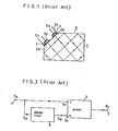
- FIG. 1 shows an example of conventional delay line
- FIG. 2 shows an example of conventional comb filter utilizing the delay line of FIG. 1
- FIG. 3 is a diagram showing a characteristic curve of the conventional comb filter of FIG. 2.
- An ultrasonic delay line shown in FIG. 1 comprises a delay element 1 which is usually made with a glass block and the oblique corner face thereof has an input terminal comprising electrodes 2a and 2b with a piezoelectric element 3 inbetween and an output terminal comprising electrodes 2a' and 2b' with a piezoelectric element 3' inbetween.
- the piezoelectric element 3 makes mechanical motion responding to the input signal E i , thereby radiating an ultrasonic wave into the delay element 1.
- the ultrasonic wave propagates in the delay element 1 making a lot of reflections at the surface thereof as shown in FIG. 1, and reaches the electrode 2b'.
- the piezoelectric element 3' By receiving the ultrasonic wave at the electrode 2b, the piezoelectric element 3' is moved and produces electric output signal E across the electrodes 2a' and 2b'.
- Such delay lines have been used in comb filters for elimination of cross color of a vide recorder signal or dot interference of an NTSC color television receiver.
- FIG. 2 shows an example of,conventional circuit construction of the comb filter using the delay line 6 as shown in FIG. 1.
- a sinusoidal input signal E A applied to the input terminal 4 is given to the delay line 6 and output signal of the delay line 6 is given to an input terminal 5b of a mixing circuit 5, and the sinusoidal input signal E A as such is applied to the other terminal 5a of the mixing circuit 5, which operates summing or subtraction of the input signals at the input terminals 5a and 5b.
- the resultant signal E C has the repetitions of peaks and valleys of its spectrum distribution with the frequency pitches of 1/ ⁇ 0 , and therefore band-path characteristic becomes comb-shaped as shown in FIG. 3, wherein the frequency pitches f' H and f" H are called comb pitches.
- the equation (6) shows that the comb filter of FIG. 2 has the comb shape characteristic having the frequency pitch of .
- the abovementioned conventional comb filter requires a certain size of the delay element block 1, and the size has been regarded particularly determined by the delay time ⁇ 0 .
- the present invention purports to provide a comb-filter realized with a smaller sized delay element in comparison with that of the conventional comb filter.
- the reducing of the size of the delay element can be made by improved configuration of the circuit of the comb filter.
- a comb filter in accordance with the present invention comprises:
- FIG. 4 is a block diagram showing an example of electric circuit structure of a comb filter embodying the present invention and FIG. 5 is an elevation view of a delay line 9 of the comb filter of FIG. 4.
- input terminals 8a and 8b are connected to the input terminals 10a and 10b of the ultrasonic delay line 9 through the impedance 13 and directly, respectively.
- the input end of the impedance 13 is connected through a first amplifier 14 as a buffer to a first input terminal 16a of a mixer 15 as an operation circuit.
- the output end of the impedance 13 is connected through a second amplifier 17 as a buffer to a second input terminal 16b of the mixer 15.
- the input terminals 8a and 8b form input terminals of the comb filter of the present invention.
- the output terminal 18 of the mixer 15 forms an output terminal of the comb filter of the present invention.
- the second amplifier 17 receives a signal of 1 ⁇ 2 ⁇ (t) from the junction point between the impedance 13 and the delay line 9 through a line 17a.
- the amplifier 17 amplifies to ⁇ 2 times the signal of 1 ⁇ 2 ⁇ (t) and gives the input terminal 16b of the mixer ' 15 the amplified output signal of
- the input terminals 10a and 10b of the delay line 9 receive the signal of 1 ⁇ 2 ⁇ (t), which actuate the piezoelectric element 19 between the electrodes 53a and 53b. That is, the signal of 1 ⁇ 2 ⁇ (t) is electromagnetically transformed to an ultrasonic wave, which is radiated into and propagates in the delay element 52, along a path as shown by the solid arrow lines reflected many times, and reaches the reflection face 521. The ultrasonic wave is reflected by the reflection face 521 and travels back on the same path but in the inverse direction, namely travelling round trip, as shown by the dotted arrow lines, and reaches the electrode 53b. Thereby, the electrode 53b and the piezoelectric element 19 are actuated and generates the following electric signal E D at the electrode 53b: where:
- the output signal of the delay line 9 output from the terminal 10a is led through the lead wire 17a to the amplifier 17, and amplified ⁇ 2 times, thereby giving the input terminal 16b the signal of
- the mixer 15 receives the signal of expression (11) at the input terminal 16a and the signals of expressions (12) and (14) at'the input terminal 16b.
- the mixer 15 operates subtraction between the signal to the input terminal 16a and the signals to the input terminal 16b, and produces the following resultant signal E C (t):
- the frequency characteristic of the equation (18) is identical to that shown by the equation (6 ) for the conventional comb filter of FIG. 2.
- FIG. 6 shows a detailed circuit construction of the comb filter elucidated referring to FIGs. 4 and 5.
- an impedance matching circuit 24 comprises a capacitor 25, resistors 26, 27 and 28 and a transistor 29.
- the amplifier 14 comprises a transistor 33 and resistors 31 and 32 and has the amplification factor ⁇ 1 .
- the amplifier 17 comprises a transistor 37, resistor 35, a capacitor 361 and a potentiometer 36 which is for adjusting the amplification factor ⁇ 2 .
- the mixer circuit 15 comprises the amplifier 17, a transistor 40 and a resistor 39 and serves as an operation circuit.
- the variable impedance 13 comprises resistors 42, 43, a capacitor 44 and a variable capacitor 45.
- the ultrasonic delay line 9 has only common electrode 10a and 10b, which is for inputting and outputting.
- the transistor 37 works as the transistor of the amplifier 17 and also as an active element of the mixer circuit 15.
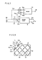
- FIG. 7 is a circuit diagram of a modified example of a comb filter embodying the present invention and FIG. 8 is an elevation view of a delay line 9' used in the comb filter of FIG. 7.
- the embodiment is almost the same to that of FIGs. 4, 5 and 6, but only difference is that the delay line 9' is slightly different from that 9 of FIGs. 4 to 6. That is, the delay line 9' of this modified example of FIGs. 7 and 8, a second set of electrodes 54a and 54b with a piezoelectric element 21 inbetween, wherein the electrode 54b is at the reflection face 521. That is, the configuration of the ultrasonic delay line 9' is similar to that (6) of the conventional one shown in FIG. 1.
- an adjustment switch 11 is provided across the electrodes 54a and 54b so as to short- circuit or open them.
- acoustic or mechanical characteristic of the piezoelectric element can be varied, and therefore, the delay time can be adjusted, and therefore the comb pitch f' H and f" H can be varied.
- the actual circuit configuration may be the sane as of FIG. 6, except the change of numeral 9 to 9' for the delay line which comprises the second terminal 12a and 12b and switch 11.
- the delay line block 52 of smaller size than the corresponding conventional one can give the same delay time. And therefore, by adopting the new circuit configuration of FIG. 4 or 6, the small size delay line 9 or 9' can be utilized, thereby reducing the size of the over-all comb filter.
Landscapes
- Physics & Mathematics (AREA)
- Acoustics & Sound (AREA)
- Piezo-Electric Or Mechanical Vibrators, Or Delay Or Filter Circuits (AREA)
- Processing Of Color Television Signals (AREA)
Applications Claiming Priority (2)
| Application Number | Priority Date | Filing Date | Title |
|---|---|---|---|
| JP8554880A JPS5710516A (en) | 1980-06-23 | 1980-06-23 | Comb type filter |
| JP85548/80 | 1980-06-23 |
Publications (3)
| Publication Number | Publication Date |
|---|---|
| EP0043048A2 true EP0043048A2 (de) | 1982-01-06 |
| EP0043048A3 EP0043048A3 (en) | 1982-01-13 |
| EP0043048B1 EP0043048B1 (de) | 1985-10-09 |
Family
ID=13861894
Family Applications (1)
| Application Number | Title | Priority Date | Filing Date |
|---|---|---|---|
| EP81104735A Expired EP0043048B1 (de) | 1980-06-23 | 1981-06-19 | Kammfilter |
Country Status (4)
| Country | Link |
|---|---|
| US (1) | US4492928A (de) |
| EP (1) | EP0043048B1 (de) |
| JP (1) | JPS5710516A (de) |
| DE (1) | DE3172589D1 (de) |
Families Citing this family (5)
| Publication number | Priority date | Publication date | Assignee | Title |
|---|---|---|---|---|
| SE436228B (sv) * | 1982-11-24 | 1984-11-19 | Bengt Hjalmar Tornblom | Anordning for kontroll av objekt med avseende pa forendringar |
| JPS61131127U (de) * | 1985-02-01 | 1986-08-16 | ||
| US4734662A (en) * | 1986-03-11 | 1988-03-29 | Tdk Corporation | Comb filter |
| JPH0614503Y2 (ja) * | 1989-09-08 | 1994-04-13 | 旭硝子株式会社 | 超音波遅延線の調整回路およびそれを内蔵した超音波遅延線素子 |
| US5436882A (en) * | 1993-01-04 | 1995-07-25 | Taddeo; Anthony R. | Method and device for improving digital audio sound |
Family Cites Families (8)
| Publication number | Priority date | Publication date | Assignee | Title |
|---|---|---|---|---|
| US2596460A (en) * | 1946-04-05 | 1952-05-13 | Us Navy | Multichannel filter |
| US2839731A (en) * | 1953-01-14 | 1958-06-17 | Bell Telephone Labor Inc | Multi-facet ultrasonic delay line |
| JPS4890647A (de) * | 1971-05-14 | 1973-11-26 | Matsushita Electric Industrial Co Ltd | |
| DE2320742A1 (de) * | 1972-06-02 | 1973-12-13 | Gte International Inc | Verzoegerungsleitung |
| US3857113A (en) * | 1974-01-30 | 1974-12-24 | Rca Corp | Microwave acoustic delay line |
| GB1524356A (en) * | 1974-11-18 | 1978-09-13 | Rca Corp | Corporation sync separator |
| US3969757A (en) * | 1975-04-21 | 1976-07-13 | Rca Corporation | Color image signal processing circuits |
| US4350956A (en) * | 1980-10-20 | 1982-09-21 | General Electric Company | Level shifting and filtering circuit |
-
1980
- 1980-06-23 JP JP8554880A patent/JPS5710516A/ja active Granted
-
1981
- 1981-06-12 US US06/272,919 patent/US4492928A/en not_active Expired - Fee Related
- 1981-06-19 EP EP81104735A patent/EP0043048B1/de not_active Expired
- 1981-06-19 DE DE8181104735T patent/DE3172589D1/de not_active Expired
Also Published As
| Publication number | Publication date |
|---|---|
| EP0043048B1 (de) | 1985-10-09 |
| DE3172589D1 (en) | 1985-11-14 |
| EP0043048A3 (en) | 1982-01-13 |
| US4492928A (en) | 1985-01-08 |
| JPS5710516A (en) | 1982-01-20 |
| JPS634366B2 (de) | 1988-01-28 |
Similar Documents
| Publication | Publication Date | Title |
|---|---|---|
| US4203082A (en) | Surface acoustic wave filter | |
| US4307356A (en) | Surface acoustic wave device | |
| EP0043048B1 (de) | Kammfilter | |
| US4954795A (en) | Surface acoustic wave filter for suppressing surface to surface interference for a satellite communication receiver | |
| US5136266A (en) | Surface acoustic wave device having staggered dispersive delay transducers | |
| EP0031685B1 (de) | Akustische Oberflächenwellenvorrichtung | |
| US4013834A (en) | Ghost signal erasing system | |
| US4263571A (en) | Surface acoustic wave filter | |
| KR100656672B1 (ko) | 탄성 표면파 장치 및 통신 기기 | |
| US3697899A (en) | Acoustic surface wave transmission device | |
| GB2123637A (en) | Surface acoustic wave device | |
| US5818310A (en) | Series-block and line-width weighted saw filter device | |
| JPS63260313A (ja) | 弾性表面波コンボルバ | |
| US4237432A (en) | Surface acoustic wave filter with feedforward to reduce triple transit effects | |
| US3987379A (en) | Acoustic surface wave filter having combined split-isolated and split-connected coupler | |
| RU201785U1 (ru) | Веерный фильтр на поверхностных акустических волнах | |
| US4870376A (en) | Monolithic elastic convolver output circuit | |
| JP2685537B2 (ja) | 弾性表面波装置、その製作方法、その調整方法、及びそれを用いた通信装置 | |
| KR970013666A (ko) | 표면파 공진자 | |
| US4344051A (en) | Elastic surface wave transducer and filter incorporating such a transducer | |
| JP3191551B2 (ja) | 圧電共振子 | |
| JPS6133719Y2 (de) | ||
| JP3254892B2 (ja) | トラップ回路 | |
| JPS641793Y2 (de) | ||
| JPS5834047B2 (ja) | 弾性表面波装置 |
Legal Events
| Date | Code | Title | Description |
|---|---|---|---|
| PUAI | Public reference made under article 153(3) epc to a published international application that has entered the european phase |
Free format text: ORIGINAL CODE: 0009012 |
|
| PUAL | Search report despatched |
Free format text: ORIGINAL CODE: 0009013 |
|
| 17P | Request for examination filed |
Effective date: 19811022 |
|
| AK | Designated contracting states |
Designated state(s): DE FR GB |
|
| AK | Designated contracting states |
Designated state(s): DE FR GB |
|
| GRAA | (expected) grant |
Free format text: ORIGINAL CODE: 0009210 |
|
| AK | Designated contracting states |
Designated state(s): DE FR GB |
|
| REF | Corresponds to: |
Ref document number: 3172589 Country of ref document: DE Date of ref document: 19851114 |
|
| ET | Fr: translation filed | ||
| PLBE | No opposition filed within time limit |
Free format text: ORIGINAL CODE: 0009261 |
|
| STAA | Information on the status of an ep patent application or granted ep patent |
Free format text: STATUS: NO OPPOSITION FILED WITHIN TIME LIMIT |
|
| 26N | No opposition filed | ||
| PGFP | Annual fee paid to national office [announced via postgrant information from national office to epo] |
Ref country code: GB Payment date: 19950608 Year of fee payment: 15 |
|
| PGFP | Annual fee paid to national office [announced via postgrant information from national office to epo] |
Ref country code: FR Payment date: 19950609 Year of fee payment: 15 |
|
| PGFP | Annual fee paid to national office [announced via postgrant information from national office to epo] |
Ref country code: DE Payment date: 19950617 Year of fee payment: 15 |
|
| PG25 | Lapsed in a contracting state [announced via postgrant information from national office to epo] |
Ref country code: GB Effective date: 19960619 |
|
| GBPC | Gb: european patent ceased through non-payment of renewal fee |
Effective date: 19960619 |
|
| PG25 | Lapsed in a contracting state [announced via postgrant information from national office to epo] |
Ref country code: FR Effective date: 19970228 |
|
| PG25 | Lapsed in a contracting state [announced via postgrant information from national office to epo] |
Ref country code: DE Effective date: 19970301 |
|
| REG | Reference to a national code |
Ref country code: FR Ref legal event code: ST |