EP0043191A1 - Magnétomètre à domaine porteur - Google Patents
Magnétomètre à domaine porteur Download PDFInfo
- Publication number
- EP0043191A1 EP0043191A1 EP81302508A EP81302508A EP0043191A1 EP 0043191 A1 EP0043191 A1 EP 0043191A1 EP 81302508 A EP81302508 A EP 81302508A EP 81302508 A EP81302508 A EP 81302508A EP 0043191 A1 EP0043191 A1 EP 0043191A1
- Authority
- EP
- European Patent Office
- Prior art keywords
- temperature
- domain
- region
- variation
- current
- Prior art date
- Legal status (The legal status is an assumption and is not a legal conclusion. Google has not performed a legal analysis and makes no representation as to the accuracy of the status listed.)
- Withdrawn
Links
Images



Classifications
-
- G—PHYSICS
- G01—MEASURING; TESTING
- G01R—MEASURING ELECTRIC VARIABLES; MEASURING MAGNETIC VARIABLES
- G01R33/00—Arrangements or instruments for measuring magnetic variables
- G01R33/02—Measuring direction or magnitude of magnetic fields or magnetic flux
- G01R33/06—Measuring direction or magnitude of magnetic fields or magnetic flux using galvano-magnetic devices
Definitions
- This invention relates to carrier-domain magnetometerso
- a carrier-domain magnetometer comprises a semiconductor device incorporating a p-n-p-n structure of circular geometry, a power source for applying a reverse bias voltage across the central p-n junction of said structure and feeding respective currents to the end p-region and the end n-region of said structure so that current flow in the device occurs in a limited domain which subtends a small angle at the central axis of said structure; and means for deriving from the device a signal which will have different magnitudes for different angular positions of the domain with respect to the central axis.
- the carrier domain will rotate continuously around the central axis at a rate dependent on the flux density parallel to that axis; this will give rise to a cyclic variation in the signal derived from the semiconductor device, the frequency of which gives a measure of flux density.
- rotation of the carrier domain would occur for any value of the flux density, but in practice it is found that there is a threshold value (dependent on the precise electrical bias conditions) below which rotation does not occur, because inescapable inhomogeneities in the device structure tend to cause the carrier domain to stick at a particular angular position.
- the domain rotation frequency is substantially directly proportional to flux density.
- a problem that occurs in the operation of a carrier-domain magnetometer is that of sensitivity of the frequency/flux density characteristic to variations in the operating conditions (temperature and electrical bias conditions) of the semiconductor device.
- temperature variations for example, it is found that in general with increasing temperature the threshold value of flux density increases, and the slope of the linear part of the characteristic decreases; in particular the slope may be reduced by about 30% for a 25°C increase in temperature.
- accurate measurements of flux density are to be made with a carrier-domain magnetometer it is necessary either to control closely the temperature and electrical bias conditions of the semiconductor device or to provide some form of compensation in respect of variations in these factors. While sufficiently close control of the bias conditions can normally be achieved by means of conventional stabilisation techniques, a similarly close control of temperature would not be feasible in many applications of the magnetometer, for example those in which the semiconductor device must be exposed to normal ambient conditions.
- the form of compensation incorporated in the invention has the further advantage that it takes the form of an electric circuit which can conveniently be integrated with the semiconductor device on a semiconductor chip.
- the power source is arranged to vary said reverse bias voltage with temperature so as to reduce the variation with temperature of the frequency of domain rotation in the presence of a magnetic field directed parallel to the central axis of said structure over a range of temperature variation, and to maintain the domain rotation frequency of the device substantially in the middle of its range of . variation with said reverse bias voltage throughout said range of temperature variation.
- the power source is also arranged to vary the current fed to the end p-region and/or the end n-region of said structure so as further to reduce the variation of domain rotation frequency with temperature.
- the magnetometer to be described utilises a semiconductor device of the type which is the subject of British Patent Specification No. 2,004,117, the device being illustrated in Figures 1 and 2.
- the device incorporates a semiconductor body in the form of a silicon chip having parallel planar main faces, only one of which (referenced 1) is shown in the drawing.
- the basic material 2 of the chip is n-type, of resistivity about two ohm-cm, and in the completed device this material serves to form the collector region of an n-p-n transistor structure and the base region of a p-n-p transistor structure.
- regions 3, 4, 5 and 6 are formed in the chip by diffusion of appropriate impurities through the face 1, the regions 3 and 4 being p-type and the regions 5 and 6 being n-type of low resistivity; the region 3 is of substantially cylindrical form, while the regions 4, 5 and 6 are of annular forms coaxial with the region 3.
- the regions 3 and 5 respectively serve as the emitter regions of the p-n-p and n-p-n transistor structures, the region 4 serves to form the collector region of the p-n-p structure and the base region of the n-p-n structure, and the region 6 serves to provide a low resistance non-rectifying contact to the region 2.
- the region 3 may have a diameter of about 120 microns
- the radial gap between the regions 3 and 4 may have a width of about two microns
- the overall radial width of the region 4 may be about 110 microns
- the region 5 may have an inner diameter of about 170 microns and a radial width of about 40 microns
- the region 6 may have an internal diameter of about 400 microns and a radial width of about 30 microns.
- the depths of the regions 3, 4, 5 and 6 are greatly exaggerated compared with their lateral dimensions; they may suitably have values of about three nicrons for the regions 3 and 4 and two microns for the regions 5 and 6.
- the diffusion processes for forming the regions 3, 4, 5 and 6 are carried out in two stages, the first using boron to form the region 3'and an annular p-type region corresponding in volume to the final regions 4 and 5 (suitably with a final sheet resistance of about 100 ohms per square) and the second using phosphorus to form the regions 5 and 6 (suitably with a final sheet resistance of about five ohms per square) and leave the remainder of the annular p-type region constituting the final region 4.
- the lateral extent of the diffusion is controlled in conventional manner by effecting the diffusion through apertures formed in an oxide layer (not shown) on the face, the oxide layer being reformed after each stage.
- the device also includes an electrode system in the form of a series of metallic conductors 7 to 14, which are formed by deposition on the chip after completion of the diffusion processes.
- the conductors 7 to 14 are deposited partly directly on the face 1, through suitable apertures formed in the oxide layer, and partly on the surface of this layer, the arrangement being such that each conductor is in direct contact with one, and only one, of the regions 3, 4, 5 and 6, the positions of which are indicated by the broken lines in Figure 2.
- the conductor 7 is in contact with the region 3 over a central circular area
- the conductor 8 is in contact with the region 5 over an area which is nearly a complete annulus but has a gap to accommodate the conductor 7
- the conductors 9 and 10 are in contact with the region 4 over diametrically opposed areas, disposed outwardly of the region 5,which between them form nearly a complete annulus but leave gaps to accommodate the conductors 7 and 8, while the conductors 11 to 14 are in contact with the region 6 over small areas respectively disposed at angular intervals of 90° around the region 6.
- the conductors 7 to 14 extend outwardly to conventional bonding pads (not shown) by means of which external connections can readily be made to the device.
- the device illustrated in Figures 1 and 2 includes a p-n-p-n structure of circular geometry constituted by the regions 3, 2, 4 and 5.
- this structure is electrically biassed so as to form a carrier domain in it.
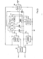
- this involves the application of a reverse bias voltage Vb from a voltage source V to the p-n junction between the regions 2 and 4 (which serves as the collector- base junction for both transistor structures), and the feeding of currents Ip and In to the regions 3 and 5 from sources 11 and 12 in such senses as to cause holes to be injected from the region 3 (p-n-p transistor emitter) into the region 2 and electrons to be injected from the region 5 (n-p-n transistor emitter) into the region 4.
- the various sources V, 11 and 12 are energised from a d.c. supply by way of a voltage regulator VR.
- a voltage regulator VR By virtue of the regenerative coupling between the two transistor structures, the actual minority carrier injection is concentrated in a domain of limited angular extent, which will be caused to rotate around the central axis of the structure if the device is subjected to a sufficiently strong magnetic field directed substantially parallel to this axis.
- the rotation of the carrier domain will give rise to cyclic variations in the individual currents flowing through the conductors 11 to 14, so that the rotation can be sensed by an output stage OS supplied with one or more (two in Figure 3) of the signals developed across loads L connected with the conductors 11 to 14, these signals being in the form of trains of current pulses whose recurrence frequency is equal to the domain rotation frequency.
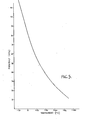
- the domain rotation frequency of a typical p-n-p-n structure varies with the temperature of the p-n-p-n structure as shown in Figure 5.
- compensation for this is provided by arranging for the biasses supplied by the sources V, 11 and 12 to vary with temperature.
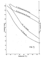
- FIG. 6 shows the variation of domain rotation frequency with the bias voltage Vb at various temperatures. It will be seen from Figure 6 that domain rotation frequency is proportional to bias voltage Vb over an appreciable range, and that by increasing bias voltage Vb along line AB with increase of temperature and vice versa the variation domain rotation frequency is only from 78 kHz to 23 kHz over a temperature range -20°C to 90°C compared with a variation of from 12 kHz to over 110 kHz with constant biasses, as shown in Figure 5.
- the working point is maintained approximately in the middle of the dynamic range of Vb which is important when it is desired to control domain rotation frequency by variation of the voltage across the p-n junction between regions 2 and 4 as well, or instead of, applied magnetic field.
- domain rotation frequency is approximately proportional to current Ip so that temperature compensation can be effected by increasing current Ip with temperature.
- Ip The upper limit for Ip is chosen in conjunction with In, as described above, and the lower limit in dependence on the value of voltage bias Vb applied at minimum temperature. In a typical arrangement Ip is arranged to vary over the range 10 to 20 milliamps.
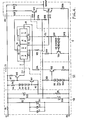
- the voltage regulator VR is of conventional form and comprises resistors R1 to R3, capacitors 01 and C2 and zener diodes 2D1 to 1D3 to produce three constant voltage outputs across diodes ZD1, ZD2 and ZD3 respectively.
- the current source 11 comprises a transistor TR1 which is connected in a constant current source configuration and drives a transistor TR2 whose collector current constitutes the current Ip.
- the required variation of Ip with temperature is obtained due to the temperature sensitivity of the base-emitter junctions of transistors TR1 and TR2 and diodes D1 to D4 connected in the emitter-base junction biassing arrangement of transistor TR1. With rise in temperature the collector current of transistor TR1 increases which drives transistor TR2 to heavier conduction and increases bias current Ip.
- the current source 12 comprises a transistor rR3 connected in a constant current configuration whose collector current constitutes the current In.
- the required variation of In with temperature is obtained due to the temperature sensitivity of diodes D5 to D8 connected in the emitter-base biassing arrangement of transistor TR3. With rise in temperature increased current flows through diodes D5 to D8 with corresponding reduction in the base current of transistor TR3, and hence a reduction in bias current In.
- the voltage Vb is derived from the collector of a transistor TR4 connected in a negative feedback arrangement to stabilize the voltage across collector load resistor RIO.
- Vb with temperature is obtained due to the temperature sensitivity of the base-emitter junction of transistor TR4 and diodes D9 to D12 connected in series between the base of transistor TR4 and the junction of two resistors R11 and R12 which are connected in series between the collector and emitter of transistor TR4.
- the output stage OS comprises two transistors TR5 and TR6 provided with respective collector loads R18 and R19 and sharing a common emitter resistor R20, the output being derived from the collector of one of the transistors (TR6).
- the bases of the transistors TR5 and TR6 are connected via respective resistors R16 and R17 to oppositely positioned ones 11 and 13 of the four conductors 11 to 14, the other two conductors 12 and 14 being connected to a reference potential via a common load resistor R13, and the conductors 11 and 13 to the same reference potential via respective load resistors R15 and R14.
- Figure 9 shows the variation of domain rotation frequercy with temperature of the magnetometer shown in Figure 4 under typical operating conditions.
- the degree of temperature compensation effected by each of the sources V, I1 and 12 can conveniently be altered by altering the number of temperature sensitive diodes incorporated in that source.
- the sources V, I1 and 12 are suitably fabricated in integrated circuit form on the same silicon chip as the p-n-p-n structure.
- the diodes D1 to D12 and transistors TR1 to TR4 will then all be accurately at the same temperature as the p-n-p-n structure providing fast temperature compensation with temperature change.
- the voltage regulator VR is preferably mounted away from the silicon chip, but the output stage OS may conveniently be fabricated thereon.
Landscapes
- Physics & Mathematics (AREA)
- Condensed Matter Physics & Semiconductors (AREA)
- General Physics & Mathematics (AREA)
- Measuring Magnetic Variables (AREA)
Applications Claiming Priority (2)
| Application Number | Priority Date | Filing Date | Title |
|---|---|---|---|
| GB8020760 | 1980-06-25 | ||
| GB8020760 | 1980-06-25 |
Publications (1)
| Publication Number | Publication Date |
|---|---|
| EP0043191A1 true EP0043191A1 (fr) | 1982-01-06 |
Family
ID=10514305
Family Applications (1)
| Application Number | Title | Priority Date | Filing Date |
|---|---|---|---|
| EP81302508A Withdrawn EP0043191A1 (fr) | 1980-06-25 | 1981-06-05 | Magnétomètre à domaine porteur |
Country Status (3)
| Country | Link |
|---|---|
| EP (1) | EP0043191A1 (fr) |
| AU (1) | AU7186381A (fr) |
| GB (1) | GB2078379A (fr) |
Cited By (1)
| Publication number | Priority date | Publication date | Assignee | Title |
|---|---|---|---|---|
| CH658916A5 (de) * | 1982-09-13 | 1986-12-15 | Landis & Gyr Ag | Magnetfeldsensor. |
Families Citing this family (1)
| Publication number | Priority date | Publication date | Assignee | Title |
|---|---|---|---|---|
| US4801883A (en) * | 1986-06-02 | 1989-01-31 | The Regents Of The University Of California | Integrated-circuit one-way isolation coupler incorporating one or several carrier-domain magnetometers |
Citations (2)
| Publication number | Priority date | Publication date | Assignee | Title |
|---|---|---|---|---|
| FR1391853A (fr) * | 1964-01-21 | 1965-03-12 | Varian Associates | Dispositif de détection d'un champ magnétique |
| GB2004117A (en) * | 1977-09-08 | 1979-03-21 | Manley M | Semiconductor devices |
-
1981
- 1981-06-03 GB GB8117045A patent/GB2078379A/en not_active Withdrawn
- 1981-06-05 EP EP81302508A patent/EP0043191A1/fr not_active Withdrawn
- 1981-06-16 AU AU71863/81A patent/AU7186381A/en not_active Abandoned
Patent Citations (2)
| Publication number | Priority date | Publication date | Assignee | Title |
|---|---|---|---|---|
| FR1391853A (fr) * | 1964-01-21 | 1965-03-12 | Varian Associates | Dispositif de détection d'un champ magnétique |
| GB2004117A (en) * | 1977-09-08 | 1979-03-21 | Manley M | Semiconductor devices |
Cited By (1)
| Publication number | Priority date | Publication date | Assignee | Title |
|---|---|---|---|---|
| CH658916A5 (de) * | 1982-09-13 | 1986-12-15 | Landis & Gyr Ag | Magnetfeldsensor. |
Also Published As
| Publication number | Publication date |
|---|---|
| GB2078379A (en) | 1982-01-06 |
| AU7186381A (en) | 1982-01-07 |
Similar Documents
| Publication | Publication Date | Title |
|---|---|---|
| US4987467A (en) | Integratable hall element | |
| US4355344A (en) | Protective device electronic semiconductor component | |
| US6144085A (en) | Power transistor device having hot-location and cool-location temperature sensors | |
| EP0018750B1 (fr) | Magnétomètres à domaines magnétiques | |
| US4131928A (en) | Voltage clamp device for monolithic circuits | |
| US5468673A (en) | Avalanche diode incorporated in a bipolar integrated circuit | |
| US4103181A (en) | Monolithic integrated transistor and protective circuit therefor | |
| US4011469A (en) | Hall effect-switching device | |
| US4040081A (en) | Alternating current control circuits | |
| CA1115854A (fr) | Semiconducteurs | |
| US3531655A (en) | Electrical signal comparator | |
| US3040266A (en) | Surface field effect transistor amplifier | |
| JPH0821633B2 (ja) | ラッチアップ保護回路 | |
| GB2078379A (en) | Carrier-domain magnetometers | |
| US5296732A (en) | Bipolar transistor | |
| US3260900A (en) | Temperature compensating barrier layer semiconductor | |
| US2996918A (en) | Junction transistor thermostat | |
| US5629551A (en) | Semiconductor device comprising an over-temperature detection element for detecting excessive temperatures amplifiers | |
| DE3325148C2 (fr) | ||
| JPH07263772A (ja) | ホール効果センサ | |
| JPH0554628B2 (fr) | ||
| JP2778076B2 (ja) | トランジスタのコレクタ抵杭の測定方法 | |
| JPS6211787B2 (fr) | ||
| JPH08256019A (ja) | トランジスタの動作電流安定化回路装置 | |
| JPS586310B2 (ja) | ハンドウタイソウチ |
Legal Events
| Date | Code | Title | Description |
|---|---|---|---|
| PUAI | Public reference made under article 153(3) epc to a published international application that has entered the european phase |
Free format text: ORIGINAL CODE: 0009012 |
|
| AK | Designated contracting states |
Designated state(s): CH DE FR NL SE |
|
| RAP1 | Party data changed (applicant data changed or rights of an application transferred) |
Owner name: THE GENERAL ELECTRIC COMPANY, P.L.C. |
|
| 17P | Request for examination filed |
Effective date: 19820609 |
|
| STAA | Information on the status of an ep patent application or granted ep patent |
Free format text: STATUS: THE APPLICATION IS DEEMED TO BE WITHDRAWN |
|
| 18D | Application deemed to be withdrawn |
Effective date: 19840418 |
|
| RIN1 | Information on inventor provided before grant (corrected) |
Inventor name: ANTOSZEWSKI, EUGENIUSZ |