EP0043246B1 - Substratvorspannungsgenerator für MOS-Baustein - Google Patents
Substratvorspannungsgenerator für MOS-Baustein Download PDFInfo
- Publication number
- EP0043246B1 EP0043246B1 EP81302872A EP81302872A EP0043246B1 EP 0043246 B1 EP0043246 B1 EP 0043246B1 EP 81302872 A EP81302872 A EP 81302872A EP 81302872 A EP81302872 A EP 81302872A EP 0043246 B1 EP0043246 B1 EP 0043246B1
- Authority
- EP
- European Patent Office
- Prior art keywords
- node
- voltage
- transistor
- substrate
- negative
- Prior art date
- Legal status (The legal status is an assumption and is not a legal conclusion. Google has not performed a legal analysis and makes no representation as to the accuracy of the status listed.)
- Expired
Links
- 239000000758 substrate Substances 0.000 title claims description 56
- 230000007704 transition Effects 0.000 claims description 37
- 230000000737 periodic effect Effects 0.000 claims description 34
- 239000004065 semiconductor Substances 0.000 claims description 4
- 230000004044 response Effects 0.000 claims description 2
- 239000003990 capacitor Substances 0.000 description 16
- 230000001808 coupling effect Effects 0.000 description 3
- 230000000694 effects Effects 0.000 description 3
- XUIMIQQOPSSXEZ-UHFFFAOYSA-N Silicon Chemical compound [Si] XUIMIQQOPSSXEZ-UHFFFAOYSA-N 0.000 description 2
- 230000004913 activation Effects 0.000 description 2
- 230000008878 coupling Effects 0.000 description 2
- 238000010168 coupling process Methods 0.000 description 2
- 238000005859 coupling reaction Methods 0.000 description 2
- 229910052710 silicon Inorganic materials 0.000 description 2
- 239000010703 silicon Substances 0.000 description 2
- 230000009471 action Effects 0.000 description 1
- 230000008859 change Effects 0.000 description 1
- 230000001419 dependent effect Effects 0.000 description 1
- 238000002347 injection Methods 0.000 description 1
- 239000007924 injection Substances 0.000 description 1
- 230000015654 memory Effects 0.000 description 1
- 238000005086 pumping Methods 0.000 description 1
- 230000035945 sensitivity Effects 0.000 description 1
Images


Classifications
-
- G—PHYSICS
- G05—CONTROLLING; REGULATING
- G05F—SYSTEMS FOR REGULATING ELECTRIC OR MAGNETIC VARIABLES
- G05F3/00—Non-retroactive systems for regulating electric variables by using an uncontrolled element, or an uncontrolled combination of elements, such element or such combination having self-regulating properties
- G05F3/02—Regulating voltage or current
- G05F3/08—Regulating voltage or current wherein the variable is DC
- G05F3/10—Regulating voltage or current wherein the variable is DC using uncontrolled devices with non-linear characteristics
- G05F3/16—Regulating voltage or current wherein the variable is DC using uncontrolled devices with non-linear characteristics being semiconductor devices
- G05F3/20—Regulating voltage or current wherein the variable is DC using uncontrolled devices with non-linear characteristics being semiconductor devices using diode- transistor combinations
- G05F3/205—Substrate bias-voltage generators
Definitions
- the invention relates to the field of metal-oxide- semi-conductor memory devices and, more particularly, to an improved substrate bias generator for random access memories.
- a negative bias voltage is typically applied to the substrate of a metal-oxide-semiconductor (MOS) random access memory (RAM) in order to improve the performance of the MOS circuit.
- MOS metal-oxide-semiconductor
- the applied negative voltage generally about minus 3.5 volts with respect to ground, lowers the junction capacitance between N+ doped silicon layers and the P- doped silicon substrate. As a result, the MOS circuit operates at a faster speed.
- the application of back bias voltage to the substrate reduces the sensitivity of the threshold voltage in the memory chip to variations in the potential between the source of an MOS transistor and the substrate bias.
- the back bias voltage was developed externally to the memory chip. More recently, back bias voltages have been generated on the chips themselves by using a charge pump to develop a negative back bias voltage. However, the charge pumps are limited to pulling the substrate potential down to a voltage in the range of minus 2.5 to minus 3.5 volts due to threshold voltage drops associated with the pump.
- GB-A-2028553 describes a bias generator for the substrate of a metal-oxide-semiconductor integrated circuit which includes a circuit reference voltage and transistors each having an inherent threshold voltage conduction point, said bias generator comprising means for generating first and second trains of periodic pulses (A, B) such that said first periodic pulses and said second periodic pulses have the same frequency and have a constant phase difference, and such that said first periodic pulses are first occurring, a first input for receiving the train of first periodic pulses, a second input for receiving the train of second periodic pulses, a first node capacitively coupled to said first input for receiving positive and negative voltage transitions derived from positive and negative amplitude transitions associated with said first pulses, a second node capacitively coupled to said second input for receiving positive and negative voltage transitions derived from positive and negative amplitude transitions associated with said second pulses, a first transistor coupled to said first and second nodes to couple voltage transitions between said first and second nodes and a second transistor coupled between the reference voltage and said first
- an improved bias generator of the above type is characterised in that said first periodic pulses have a duty cycle greater than that of said second periodic pulses, that said first transistor is biased by said reference voltage, that said second transistor is controlled by the voltage on said second node so that the clamping of said first node is in response to voltage transitions which drive the potential of said second node to a threshold voltage more positive than the reference voltage, and in that means are provided for driving the substrate voltage (E) to a voltage level slightly more positive than the voltage at said first node.
- Use of the invention may be arranged to provide an on-chip back bias generator for developing a well controlled, more negative voltage than previously obtainable so as to attain faster circuit speed and further minimise threshold voltage variations in the memory chip due to variations in the potential between the source of an MOS transistor and the substrate bias, as well as reduce the possibility of charge injection in case of the substrate being coupled more positively.
- the invention may also be used to provide an on-chip back bias generator which utilises very little power.
- the invention may also be used to provide an on-chip back bias generator which attains a faster pump down for a given frequency by achieving greater charge transfer per cycle.
- the invention may also be used to provide an on-chip back bias generator in which the substrate bias is less dependent on the threshold voltage.
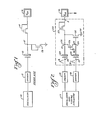
- FIG. 1 a prior art circuit used to bias the substrate of MOS integrated circuits is shown.
- the illustrated circuit includes an oscillator 10, driver 11, capacitor 12, and enhancement mode transistors 13 and 14.
- a periodic pulse generated by the oscillator 10 and driver 11 is coupled to a junction or node 15 between transistors 13 and 14 by the capacitor 12.
- the transistor 13 is turned on to clamp the potential on node 15 toward ground potential during the positive amplitude transition of the periodic pulse and is then turned off, thereby enabling the potential on node 15 to be driven negative, during the negative amplitude transition of the periodic pulse.
- This permits current to flow through transistor 14 from the substrate 16 to node 15 so as to drive the potential of the substrate 16 to a negative level.
- the preferred embodiment of the invention utilized the on-chip circuit of Figure 2 to reach and substantially maintain a more negative substrate voltage.
- This circuit includes an oscillator and timing circuitry 17 connected to drivers 18 and 19 for producing a first train of periodic pulses to an input terminal 20 and a second train of periodic pulses at an input terminal 21, respectively.
- the waveforms generated at input terminals 20 and 21 have the same frequency, approximately five megahertz in the preferred embodiment, have a constant phase difference and have amplitudes of about 5 volts.
- the waveform produced at input terminal 20 by the first train of periodic pulses has a greater duty cycle than the waveform produced at input terminal 21 by the second train of periodic pulses. Consequently, the waveforms overlap in such a manner that the waveform at input terminal 21 is enclosed within the waveform at input terminal 20.
- waveform appearing at the input terminal 20 is shown as waveform A and the waveform appearing at the input terminal 21 is shown as waveform B.
- the illustrated overlap between waveforms A and B assures that there is a sufficient time period, ten nanoseconds, for example, between the rise in voltage potential at the input terminal 21 and the rise in voltage potential at the input terminal 20, as well as a sufficient time period between the fall in voltage potential at input terminal 21 and the fall in voltage potential at input terminal 20.
- the purpose of these two time periods will become apparent from the discussion below concerning the operation of the substrate bias generator.
- a generator or pump 22 is derived by capacitors 23 and 24 and transistors 25-27.
- Node 28 is coupled via capacitor 23 to input terminal 20 so as to receive positive and negative voltage transitions derived from positive and negative amplitude transitions in the first train of periodic pulses at input terminal 20.
- node 29 is coupled via capacitor 24 to input terminal 21 so as to receive positive and negative voltage transitions derived from positive and negative amplitude transitions in the second train of periodic pulses at input terminal 21.
- the amplitude transitions of the periodic pulses at input terminals 20 and 21, illustrated by waveforms A and B drive the potentials at nodes 28 and 29, illustrated by waveforms C and D, positive and negative.
- the potentials at nodes 28 and 29 are employed to develop a negative bias voltage on the substrate 16, as illustrated by waveform E.
- Enhancement mode transistor 25 is connected between node or junction 28 and a reference voltage which may be circuit ground 30.
- Node 29 is coupled to the gate of transistor 25 for clamping node 28 to ground during the on time of each pulse in the second train of periodic pulses at input terminal 21.
- transistor 25 turns off and thereby releases the clamp on node 28.
- Enhancement mode transistor 26 is connected between nodes 28 and 29 with its gate biased to ground for coupling the potential of node 29 toward the potential of node 28. Coupling occurs only when the potential on both nodes 28 and 29 are negative and the potential on node 29 is at least a threshold voltage below the potential of the grounded gate of transistor 26.
- Enhancement mode transistor 27 is connected between node or junction 28 and substrate 16 for activation whenever the potential of node 28 is more than the threshold voltage of transistor 27 below the potential of substrate 16.
- transistor 27 When transistor 27 is turned on, current flows between the substrate 16 and node 28 so that the potential on substrate 16 is within one threshold voltage of the negative potential on node 28.
- the negative potential on node 28 is incremently coupled down to a negative voltage limit which is directly proportional to the amplitude transitions at the input terminals. Consequently, the potential on substrate 16 is incremently biased to a lower negative potential until the substrate 16 reaches a negative voltage which is offset above the negative voltage at node 28 only by the threshold voltage of transistor 27. Thereafter, this negative voltage on substrate 16 is substantially maintained. Any change in substrate voltage due to leakage is compensated for during the following pumping cycle which is described in detail below.
- the waveforms C and D indicate that nodes 28 and 29 are both negative at an arbitrary time t, (see the left-hand portion of Figure 4).
- the potential E on the substrate 16 is also negative.
- transistors 25 and 27 are turned off while transistor 26 is turned on.
- the capacitor 23 couples to the node 28 a similar positive-going amplitude transition C1.
- the potential at node 29 rises as indicated at D1 because of the on condition of transistor 26 which couples node 29 to node 28.
- This increase in potential at nodes 28 and 29 caused by the waveform A turns transistor 26 off and uncouples node 29 from node 28.
- the edge B1 of waveform B rises, and the coupling effect of the capacitor 24 causes a positive-going transition D2 to appear at node 29.
- the potential on node 29 is received by the gate of transistor 25. Therefore, when the potential on node 29 rises to a positive voltage which is more than the threshold voltage of transistor 25 above ground, transistor 25 is turned on. The activation of transistor 25 clamps or drives the potential on node 28 (which has by now risen to a 4 volt potential) down to ground potential as indicated at C2.
- waveform A undergoes a negative transition A2 which causes node 28 to be driven negative as shown at C3 due to the coupling effect of the capacitor 23.
- the transistor 26 now turns on to couple the negative transition on node 28 to node 29 so as to drive the potential at node 29 further negative to about -2 volts.
- the potential on node 28 is now more than a threshold voltage below the potential on substrate 16, whereupon transistor 27 is turned on to permit current to flow between the substrate 16 and node 28, thereby driving the potential E on substrate 16 further negative, as at E1.
- the potentials on nodes 28 and 29 are both negative and of approximately equal value due to the coupling effect of the transistor 26 which is on.
- the transistor 25 is, of course, off during this time.
- the potentials on nodes 28 and 29 remain constant until the waveform A produces another positive-going transition at time t 3 , at which time the previously discussed.cycle is repeated except for certain variations as shown in Figure 4.
- the potential on node 28 (waveform C) now starts at a lower voltage (-2 volts) than it started at on the previous cycle, and rises only to approximately the +3 volt level in the second cycle of operation.
- the potential at node 29 (waveform D) still rises to its previous level near +4 volts. The reason for this is that the potentials of nodes 28 and 29 start at a more negative potential than they did at the beginning of the previous cycle, and thus have further to rise before turning off the transistor 26.
- the transistor 26 again couples the node 29 to the node 28 for a long enough time to permit the potential at node 29 to be driven positive as indicated at D4.
- the node 29 is driven even more positive by the transition D4 than the previous positive transition D1.
- waveform A does not drive node 28 as positive during the second (time Tg)
- the node 29 is driven more negative at time t 4 by the subsequent negative-going transition of waveform A.
- the potential on the substrate 16 is also driven further negative as shown at E2.
- An increased negative voltage at node 28 and at the substrate 16 is attained on each subsequent cycle until the potential on node 28 reaches approximately -5 volts. Thereafter, the potential on substrate 16 is substantially maintained to within a threshold voltage of the -5 volt level on node 28.
- Oscillator 17 is a self-starting, three-stage oscillator which includes MOS devices 31-43.
- a Schmidt-type trigger stage 44 formed by depletion mode transistors 31 and 32 and enhancement mode transistors 33-35 acts as an inverter when a certain voltage is reached.
- the Schmidt stage 44 is used in the preferred embodiment because it requires less stages and, therefore, less power for a given frequency than a conventional ring oscillator. As a result, cleaner waveforms are provided to the drivers 18 and 19.
- the output of the Schmidt stage 44 at node 45 is delivered to the remaining oscillator stages and to driver 19.
- An RC delay path is formed by depletion mode transistor 36 and capacitor 37 at the input to the Schmidt stage 44.
- another RC delay path is formed by depletion mode transistor 38 and capacitor 39 at the output to the Schmidt stage 44.
- These delay paths set the pulse width of oscillator 17 which, in turn, determines the frequency.
- Transistor 38 and capacitor 39 are coupled to a pair of inverters 46 and 47.
- Inverter 46 formed by depletion mode transistor 40 and enhancement mode transistor 41, drives inverter 47 which is defined by depletion mode transistor 42 and enhancement mode transistor 43.
- Inverter 46 also provides a first input to driver 18 at node 48.
- Inverter 47 provides a feedback loop to oscillator 17 and a second input to driver 18 at node 49.
- Driver 18, including timing circuitry 50 and a bootstrap clock driver circuitry 51 produces a first train of periodic pulses which is delivered to input terminal 20 for creating potential transitions in the substrate bias generator 22.
- the same train of periodic pulses also acts as an input to driver 19.
- Timing circuitry 50 defined by enhancement mode transistors 52-55, is arranged as a pair of push-pull enhancement drivers for producing alternating high and low input signals at node 56 for introduction into bootstrap clock driver circuitry 51.
- Bootstrap driver 51 defined by transistors 57-63 and capacitor 64, is discussed in detail in a related U.S. Patent Application Serial Number 172766, filed July 28 1980.
- Bootstrap driver 51 basically inverts its input signal at node 56 from high to low and vice versa to provide a first train of periodic pulses at node 65 for delivery to input terminal 20 and driver 19.
- Driver 19 includes timing circuitry 66 and bootstrap clock driver 67 and produces a second train of periodic pulses at node 68 for delivery to input terminal 21.
- Timing circuitry 66 defined by enhancement mode transistors 69-74, produces alternating high and low input signals at node 68 for delivery to bootstrap driver 67.
- Timing circuitry 66 has a somewhat slower pulling down delay due to the Schmidt action created by in series transistors 72 and 73.
- Bootstrap driver 67 which is formed by associated transistors 76-82 and capacitor 83, performs similarly to bootstrap driver 51 to produce a second train of periodic pulses at node 75.
- the pulses at node 75 have a greater duty cycle than the pulses at node 68 due to the differences created by timing circuitries 50 and 66.
- oscillator 17 produces a high at node 45, a low at node 48, and a high at node 49.
- Node 45 being high ensures that node 68 will be high and that node 75 will be coresponding low thereby providing a zero voltage at input terminal 21.
- node 29 maintains its negative potential.
- node 48 The condition of node 48 being low and node 49 being high causes node 56 to be high.
- bootstrap driver 51 produces a low at node 65 for delivery to input terminal 20 and timing circuitry 66.
- Node 28 remains at its same negative potential. Since node 28 is not more than the threshold voltage of transistor 27 (approximately .6 volts) below the substrate potential, transistor 27 is off.
- oscillator 17 produces a low at node 45 which turns transistors 70 and 71 off.
- node 48 goes high and turns transistor 52 on.
- transistor 54 is turned on and thereby discharges node 56 to ground. This permits driver 18 to bootstrap node 65 high.
- Capacitor 23 couples this positive-going transition to node 28. Since node 29 is more than the threshold voltage of transistor 26 below ground, transistor 26 is on. Hence, the potential at node 29 begins to rise as described above.
- Transistor 69 is sized to give approximately the right delay time between node 65 going high and node 75 going high. Transistor 69 then causes the Schmidt trigger-type stage constituted by transistors 71-74 to discharge node 68 to ground after a certain time delay, thereby, turning off transistors 78, 80, and 82 of bootstrap driver 67 and allowing node 75 to rise. Capacitor 24 couples this positive-going transition to node 29 and transistor 25 turns on to clamp node 28 to ground.
- This low propagates through inverter 47 thereby pushing node 49 high.
- the high on node 49 propagates through source follower transistor 54, allowing node 56 to go high.
- the high at node 56 turns on transistors 59, 61 and 63, thereby disabling bootstrap driver 18 and allowing node 65 to fall.
- the delay time between node 75 falling and node 65 falling is determined by the propagation delay between the RC time constant as determined by transistors 38 and 39 and inverters 46 and 47.
- node 65 falls, this negative-going transition is coupled to node 28, and transistor 26 turns on, dragging node 29 toward the potential of node 28.
- the driving of node 29 further negative turns off clamp transistor 25 as explained above.
- transistor 27 turns on, thereby driving the substrate voltage further negative.
- the substrate potential is driven further negative. This activity of driving the substrate voltage further negative continues until node 28 cannot be driven any further negative. At this point, the substrate voltage is within transistor 27's threshold voltage of the maximum negative voltage attainable at node 28 (approximately -5 volts). During subsequent cycles, as node 28 fluctuates between a negative 5 volts and ground potential, there is leakage at the biased substrate permitting its potential to slightly increase. However, as node 28 is driven negative on the next cycle, the substrate potential returns to within a threshold voltage of node 28, i.e. approximately -4.5 volts. Therefore, the substrate bias generator substantially maintains the substrate potential within transistor 27's threshold voltage of the most negative potential reached at node 28.
Landscapes
- Engineering & Computer Science (AREA)
- Physics & Mathematics (AREA)
- Microelectronics & Electronic Packaging (AREA)
- Nonlinear Science (AREA)
- Electromagnetism (AREA)
- General Physics & Mathematics (AREA)
- Radar, Positioning & Navigation (AREA)
- Automation & Control Theory (AREA)
- Semiconductor Integrated Circuits (AREA)
- Dram (AREA)
- Logic Circuits (AREA)
Claims (6)
Applications Claiming Priority (2)
| Application Number | Priority Date | Filing Date | Title |
|---|---|---|---|
| US164284 | 1980-06-30 | ||
| US06/164,284 US4336466A (en) | 1980-06-30 | 1980-06-30 | Substrate bias generator |
Publications (2)
| Publication Number | Publication Date |
|---|---|
| EP0043246A1 EP0043246A1 (de) | 1982-01-06 |
| EP0043246B1 true EP0043246B1 (de) | 1985-09-25 |
Family
ID=22593797
Family Applications (1)
| Application Number | Title | Priority Date | Filing Date |
|---|---|---|---|
| EP81302872A Expired EP0043246B1 (de) | 1980-06-30 | 1981-06-25 | Substratvorspannungsgenerator für MOS-Baustein |
Country Status (5)
| Country | Link |
|---|---|
| US (1) | US4336466A (de) |
| EP (1) | EP0043246B1 (de) |
| JP (1) | JPS5778165A (de) |
| CA (1) | CA1176372A (de) |
| DE (1) | DE3172424D1 (de) |
Families Citing this family (31)
| Publication number | Priority date | Publication date | Assignee | Title |
|---|---|---|---|---|
| US4401897A (en) * | 1981-03-17 | 1983-08-30 | Motorola, Inc. | Substrate bias voltage regulator |
| US4403158A (en) * | 1981-05-15 | 1983-09-06 | Inmos Corporation | Two-way regulated substrate bias generator |
| EP0070667A1 (de) * | 1981-07-13 | 1983-01-26 | Inmos Corporation | Verbesserter Oszillator für Substratvorspannungsgenerator |
| US4438346A (en) | 1981-10-15 | 1984-03-20 | Advanced Micro Devices, Inc. | Regulated substrate bias generator for random access memory |
| US4439692A (en) * | 1981-12-07 | 1984-03-27 | Signetics Corporation | Feedback-controlled substrate bias generator |
| US4455493A (en) * | 1982-06-30 | 1984-06-19 | Motorola, Inc. | Substrate bias pump |
| US4581546A (en) * | 1983-11-02 | 1986-04-08 | Inmos Corporation | CMOS substrate bias generator having only P channel transistors in the charge pump |
| US4547749A (en) * | 1983-12-29 | 1985-10-15 | Motorola, Inc. | Voltage and temperature compensated FET ring oscillator |
| US4670669A (en) * | 1984-08-13 | 1987-06-02 | International Business Machines Corporation | Charge pumping structure for a substrate bias generator |
| JPS6153759A (ja) * | 1984-08-23 | 1986-03-17 | Fujitsu Ltd | 発振回路 |
| NL8402764A (nl) * | 1984-09-11 | 1986-04-01 | Philips Nv | Schakeling voor het opwekken van een substraatvoorspanning. |
| US4701637A (en) * | 1985-03-19 | 1987-10-20 | International Business Machines Corporation | Substrate bias generators |
| US4670668A (en) * | 1985-05-09 | 1987-06-02 | Advanced Micro Devices, Inc. | Substrate bias generator with power supply control means to sequence application of bias and power to prevent CMOS SCR latch-up |
| US4942312A (en) * | 1985-08-19 | 1990-07-17 | Eastman Kodak Company | Integrated-circuit having two NMOS depletion mode transistors for producing stable DC voltage |
| JPS62196861A (ja) * | 1986-02-24 | 1987-08-31 | Mitsubishi Electric Corp | 内部電位発生回路 |
| DE8714849U1 (de) * | 1986-12-23 | 1987-12-23 | Jenoptik Jena Gmbh, Ddr 6900 Jena | Geregelter CMOS-Substratspannungsgenerator |
| KR910004737B1 (ko) * | 1988-12-19 | 1991-07-10 | 삼성전자 주식회사 | 백바이어스전압 발생회로 |
| JPH04274084A (ja) * | 1991-02-27 | 1992-09-30 | Toshiba Corp | 基板電位調整装置 |
| IT1252623B (it) * | 1991-12-05 | 1995-06-19 | Sgs Thomson Microelectronics | Dispositivo a semiconduttore comprendente almeno un transistor di potenza e almeno un circuito di comando, con circuito di isolamento dinamico,integrati in maniera monolitica nella stessa piastrina |
| US5347171A (en) * | 1992-10-15 | 1994-09-13 | United Memories, Inc. | Efficient negative charge pump |
| US5412257A (en) * | 1992-10-20 | 1995-05-02 | United Memories, Inc. | High efficiency N-channel charge pump having a primary pump and a non-cascaded secondary pump |
| JPH076581A (ja) * | 1992-11-10 | 1995-01-10 | Texas Instr Inc <Ti> | 基板バイアス・ポンプ装置 |
| JP2560983B2 (ja) * | 1993-06-30 | 1996-12-04 | 日本電気株式会社 | 半導体装置 |
| US5483205A (en) * | 1995-01-09 | 1996-01-09 | Texas Instruments Incorporated | Low power oscillator |
| DE19623829C2 (de) * | 1996-06-14 | 1998-06-10 | Siemens Ag | Schaltungsanordnung zur Spannungsumpolung in einem Mobilfunkgerät |
| US5818289A (en) * | 1996-07-18 | 1998-10-06 | Micron Technology, Inc. | Clocking scheme and charge transfer switch for increasing the efficiency of a charge pump or other circuit |
| US6064250A (en) | 1996-07-29 | 2000-05-16 | Townsend And Townsend And Crew Llp | Various embodiments for a low power adaptive charge pump circuit |
| JP3019805B2 (ja) * | 1997-06-19 | 2000-03-13 | 日本電気株式会社 | Cmos論理回路 |
| US7737666B2 (en) * | 2003-08-04 | 2010-06-15 | Marvell World Trade Ltd. | Split gate drive scheme to improve reliable voltage operation range |
| JP3902769B2 (ja) * | 2003-08-29 | 2007-04-11 | 松下電器産業株式会社 | 降圧電圧出力回路 |
| KR102613318B1 (ko) * | 2015-12-28 | 2023-12-14 | 가부시키가이샤 한도오따이 에네루기 켄큐쇼 | 반도체 장치 |
Family Cites Families (5)
| Publication number | Priority date | Publication date | Assignee | Title |
|---|---|---|---|---|
| US4142114A (en) * | 1977-07-18 | 1979-02-27 | Mostek Corporation | Integrated circuit with threshold regulation |
| DE2812378C2 (de) * | 1978-03-21 | 1982-04-29 | Siemens AG, 1000 Berlin und 8000 München | Substratvorspannungsgenerator für integrierte MIS-Schaltkreise |
| US4229667A (en) * | 1978-08-23 | 1980-10-21 | Rockwell International Corporation | Voltage boosting substrate bias generator |
| US4208595A (en) * | 1978-10-24 | 1980-06-17 | International Business Machines Corporation | Substrate generator |
| JPS5951749B2 (ja) * | 1978-11-17 | 1984-12-15 | 富士通株式会社 | 基板バイアス発生回路 |
-
1980
- 1980-06-30 US US06/164,284 patent/US4336466A/en not_active Expired - Lifetime
-
1981
- 1981-03-17 CA CA000373211A patent/CA1176372A/en not_active Expired
- 1981-06-25 DE DE8181302872T patent/DE3172424D1/de not_active Expired
- 1981-06-25 EP EP81302872A patent/EP0043246B1/de not_active Expired
- 1981-06-29 JP JP56099800A patent/JPS5778165A/ja active Pending
Also Published As
| Publication number | Publication date |
|---|---|
| US4336466A (en) | 1982-06-22 |
| JPS5778165A (en) | 1982-05-15 |
| CA1176372A (en) | 1984-10-16 |
| DE3172424D1 (en) | 1985-10-31 |
| EP0043246A1 (de) | 1982-01-06 |
Similar Documents
| Publication | Publication Date | Title |
|---|---|---|
| EP0043246B1 (de) | Substratvorspannungsgenerator für MOS-Baustein | |
| US4617529A (en) | Ring oscillator with delay element and potential pulling circuit | |
| EP0150480A2 (de) | Impulsgenerator zur Grundzustandseinstellung bei Netzeinschaltung | |
| US5247208A (en) | Substrate bias generating device and operating method thereof | |
| US5359244A (en) | Gate drive circuit for a MOS power transistor | |
| EP0445083B1 (de) | Spannungserhöhte Phasen-Oszillator für den Antrieb eines Spannungsvervielfachers | |
| US4812687A (en) | Dual direction integrating delay circuit | |
| US4894559A (en) | Buffer circuit operable with reduced power consumption | |
| US4472645A (en) | Clock circuit for generating non-overlapping pulses | |
| WO1999014857A1 (en) | Boosted voltage driver | |
| US4239991A (en) | Clock voltage generator for semiconductor memory | |
| US5398001A (en) | Self-timing four-phase clock generator | |
| JPH06150652A (ja) | 半導体集積回路 | |
| US20020075038A1 (en) | Active leakage control technique for high performance dynamic circuits | |
| JPH03283182A (ja) | 半導体昇圧回路 | |
| EP0070667A1 (de) | Verbesserter Oszillator für Substratvorspannungsgenerator | |
| US5808484A (en) | Method and apparatus for detecting changes in a clock signal to static states | |
| US4496852A (en) | Low power clock generator | |
| KR960001076B1 (ko) | 발진 유도 회로 | |
| US6903592B2 (en) | Limited variable width internal clock generation | |
| US3585408A (en) | Mosfet circuit for extending the time duration of a clock pulse | |
| KR100452636B1 (ko) | 반도체 메모리 장치용 클럭 발생기 | |
| JPH03102911A (ja) | クロック信号発生回路 | |
| JPH0681025B2 (ja) | ゲ−ト駆動回路 | |
| KR100203867B1 (ko) | 차아지 펌프회로를 이용한 신호 지연 회로 |
Legal Events
| Date | Code | Title | Description |
|---|---|---|---|
| PUAI | Public reference made under article 153(3) epc to a published international application that has entered the european phase |
Free format text: ORIGINAL CODE: 0009012 |
|
| AK | Designated contracting states |
Designated state(s): BE CH DE FR GB IT NL SE |
|
| 17P | Request for examination filed |
Effective date: 19820622 |
|
| RAP1 | Party data changed (applicant data changed or rights of an application transferred) |
Owner name: INMOS CORPORATION |
|
| GRAA | (expected) grant |
Free format text: ORIGINAL CODE: 0009210 |
|
| AK | Designated contracting states |
Designated state(s): BE CH DE FR GB IT LI NL SE |
|
| PG25 | Lapsed in a contracting state [announced via postgrant information from national office to epo] |
Ref country code: LI Effective date: 19850925 Ref country code: IT Free format text: LAPSE BECAUSE OF FAILURE TO SUBMIT A TRANSLATION OF THE DESCRIPTION OR TO PAY THE FEE WITHIN THE PRESCRIBED TIME-LIMIT;WARNING: LAPSES OF ITALIAN PATENTS WITH EFFECTIVE DATE BEFORE 2007 MAY HAVE OCCURRED AT ANY TIME BEFORE 2007. THE CORRECT EFFECTIVE DATE MAY BE DIFFERENT FROM THE ONE RECORDED. Effective date: 19850925 Ref country code: CH Effective date: 19850925 Ref country code: BE Effective date: 19850925 |
|
| PG25 | Lapsed in a contracting state [announced via postgrant information from national office to epo] |
Ref country code: SE Effective date: 19850930 |
|
| REF | Corresponds to: |
Ref document number: 3172424 Country of ref document: DE Date of ref document: 19851031 |
|
| ET | Fr: translation filed | ||
| REG | Reference to a national code |
Ref country code: CH Ref legal event code: PL |
|
| PLBE | No opposition filed within time limit |
Free format text: ORIGINAL CODE: 0009261 |
|
| STAA | Information on the status of an ep patent application or granted ep patent |
Free format text: STATUS: NO OPPOSITION FILED WITHIN TIME LIMIT |
|
| 26N | No opposition filed | ||
| PGFP | Annual fee paid to national office [announced via postgrant information from national office to epo] |
Ref country code: NL Payment date: 20000524 Year of fee payment: 20 |
|
| PGFP | Annual fee paid to national office [announced via postgrant information from national office to epo] |
Ref country code: FR Payment date: 20000525 Year of fee payment: 20 |
|
| PGFP | Annual fee paid to national office [announced via postgrant information from national office to epo] |
Ref country code: GB Payment date: 20000530 Year of fee payment: 20 |
|
| PGFP | Annual fee paid to national office [announced via postgrant information from national office to epo] |
Ref country code: DE Payment date: 20000630 Year of fee payment: 20 |
|
| PG25 | Lapsed in a contracting state [announced via postgrant information from national office to epo] |
Ref country code: GB Free format text: LAPSE BECAUSE OF EXPIRATION OF PROTECTION Effective date: 20010624 |
|
| PG25 | Lapsed in a contracting state [announced via postgrant information from national office to epo] |
Ref country code: NL Free format text: LAPSE BECAUSE OF EXPIRATION OF PROTECTION Effective date: 20010625 |
|
| REG | Reference to a national code |
Ref country code: GB Ref legal event code: PE20 Effective date: 20010624 |
|
| NLV7 | Nl: ceased due to reaching the maximum lifetime of a patent |
Effective date: 20010625 |