EP0043929A2 - Messanordnung mit optischer Fiber - Google Patents
Messanordnung mit optischer Fiber Download PDFInfo
- Publication number
- EP0043929A2 EP0043929A2 EP81104609A EP81104609A EP0043929A2 EP 0043929 A2 EP0043929 A2 EP 0043929A2 EP 81104609 A EP81104609 A EP 81104609A EP 81104609 A EP81104609 A EP 81104609A EP 0043929 A2 EP0043929 A2 EP 0043929A2
- Authority
- EP
- European Patent Office
- Prior art keywords
- measuring device
- light
- signal
- diode
- measuring
- Prior art date
- Legal status (The legal status is an assumption and is not a legal conclusion. Google has not performed a legal analysis and makes no representation as to the accuracy of the status listed.)
- Granted
Links
Images



Classifications
-
- H—ELECTRICITY
- H04—ELECTRIC COMMUNICATION TECHNIQUE
- H04B—TRANSMISSION
- H04B10/00—Transmission systems employing electromagnetic waves other than radio-waves, e.g. infrared, visible or ultraviolet light, or employing corpuscular radiation, e.g. quantum communication
- H04B10/40—Transceivers
- H04B10/43—Transceivers using a single component as both light source and receiver, e.g. using a photoemitter as a photoreceiver
-
- H—ELECTRICITY
- H04—ELECTRIC COMMUNICATION TECHNIQUE
- H04B—TRANSMISSION
- H04B10/00—Transmission systems employing electromagnetic waves other than radio-waves, e.g. infrared, visible or ultraviolet light, or employing corpuscular radiation, e.g. quantum communication
- H04B10/80—Optical aspects relating to the use of optical transmission for specific applications, not provided for in groups H04B10/03 - H04B10/70, e.g. optical power feeding or optical transmission through water
- H04B10/806—Arrangements for feeding power
- H04B10/807—Optical power feeding, i.e. transmitting power using an optical signal
-
- H—ELECTRICITY
- H10—SEMICONDUCTOR DEVICES; ELECTRIC SOLID-STATE DEVICES NOT OTHERWISE PROVIDED FOR
- H10F—INORGANIC SEMICONDUCTOR DEVICES SENSITIVE TO INFRARED RADIATION, LIGHT, ELECTROMAGNETIC RADIATION OF SHORTER WAVELENGTH OR CORPUSCULAR RADIATION
- H10F55/00—Radiation-sensitive semiconductor devices covered by groups H10F10/00, H10F19/00 or H10F30/00 being structurally associated with electric light sources and electrically or optically coupled thereto
Definitions
- the invention relates to a fibre optical measuring device according to the prior art portion of claim 1.
- the fibre optical measuring device comprises a transducer section which comprises optically supplied electronic equipment, the supply power and the measuring signal being arranged to be transmitted on the same light guide fibre.
- the device further includes light-emitting diodes (LEDs) and photo-diodes.
- the one or more light-emitting diode(s) for transmitting a measuring signal is/are transparent'to light with the wavelength A which is used for supplying the photo-diode for the power supply.
- These light-emitting diodes are located in the optical path between the fibre end and the one or more photo-diode(s) receiving the optical supply power.
- the photo-diode(s) for receiving the measuring signals is/are transparent to light with the wavelength h which is used for the supply, and these photo-diodes are located between the fibre end and the light-emitting diode(s) which deliver(s) the supply power.
- the present invention aims to improve the device according to the above-mentioned application in so far as to build up the transducer side of simpler components, to achieve better efficiency, and to eliminate the requirement to increase the voltage from one or more photo-diodes to be able to drive a light-emitting, diode.
- the invention suggests a fibre optical measuring device of the above-mentioned kind, which is characterized by the features of the characterizing portion of claim 1.
- the invention also relates to a device for carrying out a method of using a component, designated "photo-luminescence diode", which is at the same time a photo-diode and a light-emitting diode.
- a component designated "photo-luminescence diode”
- An improved efficiency is obtained since charge carriers, which are excited by light, recombine directly and emit the information-carrying light.
- the device is based on the fact that there is a concentration of optically excited minority charge carriers in the active region of an illuminated diode. There is a certain probability that the minority charge carriers will recombine with radiating recombination, which results in light being emitted.
- the process described above is called photo-luminescence, and the intensity of the light which is emitted is a function of the concentration of minority charge carriers.
- This concentration can be controlled externally by controlling the amount of charge carriers which are tapped from the active region. This can be done by changing the current-voltage operating point of the diode, for example by changing the current output from the diode.
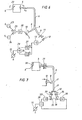
- Figure 1 shows the use of a photo-luminescence diode in an optically fed measuring device according to the invention.
- a light-emitting diode 10 feeds light of the wavelength ⁇ 1 into a light guide fibre 8. The light passes a fibre branch 7 and a fibre 6 and illuminates a photo-luminescence diode 5.
- Diode 5 supplies power to an electronic circuit 1 via a filter consisting of a resistor 3 and a capacitor 2.
- the electronic circuit 1 transforms a quantity to be measured - here designated as x and being the quantity to be measured by the device according to the invention - into coded form, for example a frequency, and controls a transistor 4 which modulates the current output from the photo-luminescence diode 5.
- the modulation is prevented from influencing the supply voltage.
- the modulation of the current outlet from photo-luminescence diode 5 also causes the photo-luminescence from 5 to.become modulated.
- the luminescence has the wavelength ⁇ 2 and is transmitted via the light guide fibre 6, the branch 7, a fibre 9 and a filter 11 to a photo-diode 12.
- the task of the filter 11 is to filter away any reflected light with the wavelength ⁇ 1 .
- the output current from the photo-diode 12 consitutes an illustration of the modulation of the photo-luminescence diode 5.
- the measuring signal After amplifying the photo-current by an amplifier 13, the measuring signal is decoded in an electronic circuit 14, shown in Figure 1 as a frequency/voltage convertor.
- the output signal from circuit 14 gives the measured value of quantity x on a measuring instrument 15.
- Figure 2 shows the spectrum from the light-emitting diode 10 designated ⁇ LED ( ⁇ ) , the transmission curve for the Filter 11 designated T( ⁇ ), and the spectrum from the photo-luminescence diode, designated ⁇ PLD ( ⁇ )
- Figure 3 shows a device with a photo-luminescence diode of GaAs/GaAlAs.
- a substrate 17 of GaAs there are formed in successive order by liquid phase epitaxy an N-layer 18 of GaAlAs, a p-doped GaAs layer 19 and a P-doped GaAlAs layer 20.
- N-layer 18 of GaAlAs a p-doped GaAs layer 19 and a P-doped GaAlAs layer 20.
- the Al content in layer 18 is so high that the transmission at the excitation wavelength is high.
- the active layer 19 is limited partly by the pN-heterojunction (two semiconductor materials having different band gaps) between layers 18 and 19, and partly by the pP-junction to layer 20. Because layer 20 is made of a material having a higher band gap, minority charge carriers are prevented from penetrating into layer 20.
- the photo-luminescence diode is contacted with metalized portions 16 and 21.
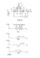
- FIG. 4 shows a short-circuited photo-luminescence diode
- Figure 5 shows a diode loaded with a resistance R L .
- the band diagram in Figure 4a shows the active layer 19 surrounded by two layers having greater band gaps, 18 and 20. Because the diode is short-circuited, there is no voltage across the pN-junction and therefore the Fermi level is constant through the structure.
- the diode is illuminated by light of the wavelength ⁇ 1 , where Eg 1 > > E g 2 (E g 1 being the band gap in layers 18 and E 2 the band gap in layer 19), the light has a high transmission through the layer 18, and the main part of the light is absorbed in the layer 19, which leads to the formation of minority charge carriers, in this case electrons.
- the electrons are prevented from penetrating into region 20 by the potential barrier which is caused by the band gap Eg 3 in layer 20 being greater than the band gap Eg 2 .
- the addition of optically excited electrons in the active region 19 is balanced by two processes.
- Electrons are passed across the pN-junction between regions 19 and 18, which gives rise to an electron flux ⁇ T from region 19, which gives the short-circuit current of the diode.
- electrons in region 19. have a certain probability to recombine with holes. Part of this recombination is radiating, which results in photons with the energy hc/ ⁇ 2 being emitted.
- the intensity of the emitted radiation depends on the concentration of the minority charge carriers in region 19.
- Figure 4b shows an equivalent diagram for a short-circuited photo-luminescence diode, where the diode is represented by a current source, which provides the short-circuit current Iph, caused by optical excitation, in parallel with an ideal diode.
- the entire optically excited current I - passes through the external short-circuit, the current through the ideal diode being zero.
- Figure 4c shows the current/voltage characteristic of the photo-luminescence diode.
- the working point for a short-circuited diode is marked by a ring in Figure 4c.
- FIG. 5a The band diagram of a photo-luminescence diode with a load resistance R L coupled across its connections is shown' in Figure 5a.
- Figure 5a differs in that a voltage is applied across the diode. The voltage is caused by the current which passes through the load resistance R L . Because the voltage V across the diode is not zero, the Fermi level varies through the diode, and the potential barrier in the pN-junction is much lower than in the case with a short-circuited diode. The low potential barrier makes it possible for majority charge carriers, electrons in region 18, to penetrate into region 19. The electrons give an electron flux ⁇ T , which is opposite to the flux ⁇ L caused by the optically excited electron surplus in 19. The electron concentration in region 19 will thus be higher than with a short-circuited diode. This leads to a higher intensity of the light from a radiating recombination in region 19.
- the electron fluxes ⁇ L and ⁇ T will cancel each other, and therefore all electrons which are formed by optical excitation will disappear through recombination in the active region 19, and the intensity of the radiating recombination is high.
- the internal quantum efficiency is determined by the number of electrons which recombine while emitting light, and the number of electrons which recombine via other processes, for example via defects in region 19 or in its limiting surfaces.
- FIG. 5b An equivalent circuit diagram of the photo-luminescence diode, coupled to a load resistance R L9 is shown in Figure 5b.
- the current I ph is divided between the ideal diode and the load resistance.
- Figure 5c shows the current/voltage characteristic of the photo-luminescence diode together with the load line of the resistance RL. The intersection between the curves defines the operating point of the circuit.
- the current from the photo-luminescence diode can be modulated. If the photo-luminescence diode is made such that the thickness of the active region 19 is smaller than the diffusion length L n (material parameter determined by the purity and quality of the material) in the active region, the concentration of minority charge carriers and thus the luminescence from the photo-luminescence diode-will be modulated at the same rate as R L .
- Figure 6 shows-a measuring device where the photo-luminescence diode 5 is used together with a transducer element 22, the frequency dependence of which is influenced by the quantity X to be measured.
- the transducer element may be inductive or capacitive and may also contain a resistive component.
- the quantity to be measured may influence the inductance, the capacitance and/or the resistance of the impedance Z.
- the mode of operation of the measuring device is as follows:
- the transducer element may consist of one or more components, the frequency properties of which are changed by the quantity to be measured.
- the frequency properties are arranged to be analyzed by measuring with several frequencies, measuring of phase shift, time delay and/or time constant to extract the measuring signal and compensate for variations in the optical transmission.
- the photo-luminescence diode in combination with resistive transducer elements can be used for direct analog measurements. Piezo-resistive materials, thermistors or magneto- diodes can operate as transducer elements. In such a system compensation must take place for variations of the transmission parameters of the optical system.
- Figure 7 shows an analog measuring system, where the photo-luminescence from the material of a layer 31 in the figure functions as a reference signal and provides a possibility of compensating for variations of the transmission para- meters of the optical system. Current is driven through a light-emitting diode 10, the emitted light of which with the wavelength ⁇ 1 is transmitted via a light guide fibre 8, a fibre branch 7, and a fibre 6 to a photo-luminescence diode 5.
- ⁇ 2 is the wavelength of the emitted light of the photo-luminescence diode 5.
- the photo-luminescence diode 5 is connected across a resistive transducer element 30, the resistance of which is controlled by the quantity X to be measured. The current through and the light from the photo-luminescence diode 5 are thereby controlled by the quantity X to be measured.
- Both, the luminescence signals of the wavelength ⁇ 2 and the wavelength ⁇ 3 are returned to the instrument side by the fibre 6, the fibre branch 7, and a light guide fibre 9.
- any components of the excitation light with the wavelength ⁇ 1 are eliminated in a filter 32.
- the light components of the wavelengths ⁇ 2 and ⁇ 3 , respectively, are separated by means of two filters 33 and 34, each component then illuminating a photo-diode 35 and 36, respectively.
- the signals from the photo-diodes are amplified in the amplifiers 37 and 38, respectively.
- the quotient between the two signals is formed in a dividing circuit 39.
- a signal proportional to the light from the photo-luminescence diode 5 is divided by a signal which is proportional to the reference signal. This reduces the dependence of the measured signal on the parameters of the optical transmission.
- the output signal from the circuit 39 gives the measured value X to the instrument 15.
- the transmitted reference signal may be used for controlling the amplification of an element in the transmission of the measuring signal.
- Figure 8 shows how the reception and the processing of the signal may be arranged in that case.
- the transmitted reference signal gives rise to a current in the photo-diode 36, the current then being amplified in a variable amplifier 46, the output signal of which is passed to a summation circuit 47.
- the difference is formed between the signal from the amplifier 46 and a reference voltage V ref .
- the difference signal is supplied to-a regulator 48, the output signal of which controls the amplification in the variable amplifier 46 so that the difference signal from the circuit/becomes zero.
- the output signal from the regulator 48 also controls the amplification in the amplifier 45, where the transmitted measuring signal from the photo-diode is amplified before being supplied to the instrument 15. If the amplifiers 45 and 46 are identical, the transmission of the measuring signal will be constant, independent of variations of the para-meters of the optical transmission.
- Figure 9a shows the emission spectra for the excitation light-emitting diode 10, ⁇ LED (A), photo-luminescence diode 5, ⁇ PLD ( ⁇ ), and the photo-luminescence material of layer 31, ⁇ PL ( ⁇ ).
- Figure 9b shows the transmission curve of the filter 32 in Figures 7 and 8.
- the filter has a high transmission for both the wavelengths ⁇ 2 and ⁇ 3 , whereas.light with the wavelength ⁇ 1 is attenuated considerably.
- the transmission curve for the filter 33 is shown in Figure 9c.
- the transmission for ⁇ 2 is high whereas light from the wavelength ⁇ 3 is greatly attenuated.
- Figure 9d shows that the transmission through the filter 34 is high at the wavelength ⁇ 3 , but low at ⁇ 2 . If the filter 34 is formed as a band pass filter around the wavelength ⁇ 3 , which attenuates ⁇ 1 and ⁇ 2 , the filter 32 can be eliminated.
- Figure 10a shows a structure where the photo-luminescence diode and the material which provides the reference signal, are located in the same component.
- Figure 10b shows the band gap for the material in the various layers. The distribution of the light intensity through the structure is shown in Figure 10c.
- Light which enters from the right is attenuated above all in the two layers with a small band gap, layers 41 and 43.
- the layers with a larger band gap 40, 42 and 44 have a high transmission for the excitation light of the wavelength ⁇ 3 . Since the layer 41 is surrounded by the layers 40 and 42 with larger band gap, minority charge carriers, holes, which are generated in the layer 41, will be contained and the efficiency in the photo-luminescence is high.
- the layer 41 shall be made so thin that only part of the excitation light is absorbed. The remaining light is absorbed for the major part in the layer 43, which constitutes-the active region of the photo-luminescence.
- the emission from the layer 43 has the wavelength ⁇ 2 ⁇ 3 and an intensity which can be controlled by the current through the photo-luminescence diode.
- the band diagram for the component in Figure 10a with short-circuited photo-luminescence diode is shown in Figure 11.
- Light of the wavelengthA which arrives from the right, passes the region 40 and generates minority charge carriers, holes, in the region 41. Some of these holes recombine with electrons, which results in photons of the wavelength ⁇ 3 being emitted.
- the part of the light which is not absorbed in the region 41 passes the region 42 and is absorbed for the most part in the region 43, where minority-charge carriers, electrons, are formed.
- the electrons will sweep out via the pN-junction between the regions 43 and 42, or recombine in the region 43.
- Part of the recombination is radiant, light of the wavelength ⁇ 2 then being emitted.
- the intensity of the emitted light is dependent on the concentration of the minority charge carriers in the region 43 and can therefore be controlled through the current taken from the diode.
- the photo-luminescence diode may, of course, be made with other barriers to control the concentration of minority charge carriers in the active region.
- hetero-pn-junction it may be made with homo-pn-junction, Schottky barrier, or MIS structure.
- the recombination may be arranged to take place in a material with a monotonously decreasing band gap along the path of the excitation light.
- the material can then be provided with a barrier, a pn-junction, a Schottky or MIS structure, which results in a depletion layer the position of which is determined by the voltage across the barrier. If the excitation light has a wavelength which causes a considerable part of the excitation of charge carriers to take place within the distance of some diffusion length from the edge of the depletion layer, the spectral distribution of the emitted light will be dependent on the voltage across the barriers.
- the photo-luminescence diode may be formed so that the active region on both sides are surrounded by controllable barriers, which will increase the possible degree of modulation for the luminescence by a factor four with a given thickness of the structure and a given diffusion length in the material.
- Measuring devices where the photo-luminescence diode is used for measuring a quantity other than the temperature, can also provide a measured value of the temperature by analyzing the spectrum of the photo-luminescence diode with methods previously proposed. (See GB patent application 803255Q)
- the temperature dependence of the measuring transducer may be adapted to be corrected by means of the measured value of the temperature.
- light as used in the foregoing description, besides relating to light within the visible area also relates to electromagnetic radiation within UV- and IR- range.
- the structure which provides the light for the signal transmission may partially be transparent to the excitation light, so that several structures can be placed one after the other in a bus structure along the optical path.
- the different structures can emit light of the same or of different wavelength, thus enabling wavelength- multiplexed transmission of the measuring signals.
Landscapes
- Physics & Mathematics (AREA)
- Electromagnetism (AREA)
- Engineering & Computer Science (AREA)
- Computer Networks & Wireless Communication (AREA)
- Signal Processing (AREA)
- Investigating, Analyzing Materials By Fluorescence Or Luminescence (AREA)
- Investigating Or Analysing Materials By Optical Means (AREA)
- Arrangements For Transmission Of Measured Signals (AREA)
- Optical Communication System (AREA)
- Testing Of Optical Devices Or Fibers (AREA)
- Light Guides In General And Applications Therefor (AREA)
- Optical Fibers, Optical Fiber Cores, And Optical Fiber Bundles (AREA)
Applications Claiming Priority (2)
| Application Number | Priority Date | Filing Date | Title |
|---|---|---|---|
| SE8004602 | 1980-06-23 | ||
| SE8004602A SE422111B (sv) | 1980-06-23 | 1980-06-23 | Fiberoptiskt kopplat metdon |
Publications (3)
| Publication Number | Publication Date |
|---|---|
| EP0043929A2 true EP0043929A2 (de) | 1982-01-20 |
| EP0043929A3 EP0043929A3 (en) | 1982-09-01 |
| EP0043929B1 EP0043929B1 (de) | 1985-12-27 |
Family
ID=20341266
Family Applications (1)
| Application Number | Title | Priority Date | Filing Date |
|---|---|---|---|
| EP81104609A Expired EP0043929B1 (de) | 1980-06-23 | 1981-06-15 | Messanordnung mit optischer Fiber |
Country Status (6)
| Country | Link |
|---|---|
| US (1) | US4417140A (de) |
| EP (1) | EP0043929B1 (de) |
| JP (1) | JPS5729009A (de) |
| CA (1) | CA1163458A (de) |
| DE (1) | DE3173291D1 (de) |
| SE (1) | SE422111B (de) |
Cited By (6)
| Publication number | Priority date | Publication date | Assignee | Title |
|---|---|---|---|---|
| EP0080318A1 (de) * | 1981-11-25 | 1983-06-01 | Western Electric Company, Incorporated | Optische Einrichtung zur Abfrage der Stellung eines Schalters |
| EP0097611A3 (de) * | 1982-06-21 | 1984-11-28 | Asea Ab | Hermetisch dichte Verbindung zwischen einem Galliumarsenidbauteil und einem Glaskörper |
| GB2177869A (en) * | 1985-06-20 | 1987-01-28 | Pirelli Cavi Spa | Remote power transmission equipment |
| EP0324349A3 (de) * | 1988-01-09 | 1989-10-18 | Conducta Gesellschaft für Mess- und Regeltechnik mbH & Co. | Verfahren und Vorrichtung zur Messwertübertragung bei elektrochemischen Sensoren |
| EP0339334A3 (en) * | 1988-04-29 | 1990-08-22 | Westinghouse Electric Corporation | Optically coupled remote sensor apparatus and system |
| EP3506533A1 (de) * | 2017-12-29 | 2019-07-03 | Nokia Technologies Oy | Erfassungsvorrichtung und -system |
Families Citing this family (27)
| Publication number | Priority date | Publication date | Assignee | Title |
|---|---|---|---|---|
| DE3126023A1 (de) * | 1981-07-02 | 1983-01-13 | Volkswagenwerk Ag, 3180 Wolfsburg | "anordnung zur gewinnung einer bewegungsinformation, insbesondere einer drehzahlinformation in einem kraftfahrzeug" |
| US4521684A (en) * | 1982-02-22 | 1985-06-04 | The Foxboro Company | Optical measurement system with light-driven vibrating sensor element |
| US4490606A (en) * | 1982-04-26 | 1984-12-25 | Geosource Inc. | Transducer apparatus utilizing fiber optics for data transmission |
| SE431260B (sv) * | 1982-06-02 | 1984-01-23 | Asea Ab | Fiberoptiskt metdon for metning av elektriska och magnetiska storheter |
| GB2144547B (en) * | 1983-08-04 | 1986-10-01 | Gen Electric Plc | A strain sensor |
| US4621929A (en) * | 1983-10-12 | 1986-11-11 | Luxtron Corporation | Fiber optic thermal anemometer |
| US4564756A (en) * | 1984-01-06 | 1986-01-14 | International Business Machines Corporation | Proximity sensor with a light-emitting diode which simultaneously emits and detects light |
| US4672199A (en) * | 1984-03-02 | 1987-06-09 | Fiberdynamics, Inc. | Fiberoptic temperature/pressure sensor system |
| US4743752A (en) * | 1984-05-07 | 1988-05-10 | The Foxboro Company | Fiber optic remote sensor |
| US4636636A (en) * | 1984-07-13 | 1987-01-13 | Sperry Corporation | Microwatt battery powered optical sensor |
| US4692607A (en) * | 1985-10-25 | 1987-09-08 | Optech Inc. | Controlled color light source |
| FR2599493A1 (fr) * | 1986-05-30 | 1987-12-04 | Comp Generale Electricite | Dispositif de mesure multipoint a fibre optique avec multiplexage temporel |
| GB8909593D0 (en) * | 1989-04-26 | 1989-06-14 | Unicon Holdings Ltd | Optical fibre sensor system |
| US5258868A (en) * | 1990-02-02 | 1993-11-02 | Rosemount Inc. | Optical process variable transmitter |
| US5345076A (en) * | 1991-11-06 | 1994-09-06 | The Boeing Company | Optically trimmed sensor for reducing influence of differential node losses |
| US5528409A (en) * | 1994-10-13 | 1996-06-18 | Nt International, Inc. | Fiber-optic interface system |
| US5965877A (en) * | 1995-04-25 | 1999-10-12 | Lockheed Martin Corporation | Photoluminescence built-in-test for optical systems |
| US5727110A (en) * | 1995-09-29 | 1998-03-10 | Rosemount Inc. | Electro-optic interface for field instrument |
| US5771114A (en) * | 1995-09-29 | 1998-06-23 | Rosemount Inc. | Optical interface with safety shutdown |
| GB9621776D0 (en) * | 1996-10-18 | 1996-12-11 | Northern Telecom Ltd | ATM communications system and method |
| DE10010556A1 (de) * | 2000-03-08 | 2001-09-13 | Bremer Sonderabfall Beratungsg | Detektor zum Messen der Dosisleistung sowie Vorrichtung zum Sortieren von Altbatterien oder Altakkumulatoren nach ihrem Typ |
| US7315162B2 (en) * | 2004-03-18 | 2008-01-01 | Elster Electricity, Llc | Reducing power consumption of electrical meters |
| DE102007047093B4 (de) * | 2007-10-01 | 2010-07-01 | Ferton Holding S.A. | Vorrichtung zur Messung von Fluoreszenzstrahlung an biologischen Substanzen mit einer Halbleitersensorenanordnung |
| RU2383865C1 (ru) * | 2008-08-13 | 2010-03-10 | Учреждение Российской академии наук Институт радиотехники и электроники им. В.А. Котельникова РАН | Оптоэлектронная измерительная система |
| CA2794231C (en) | 2012-10-31 | 2018-08-14 | Ioannidis Nektarios | Periodontal probe with touch sensing |
| CN104768454B (zh) * | 2012-11-08 | 2018-04-24 | 皇家飞利浦有限公司 | 光学探头系统 |
| US11619660B2 (en) | 2018-02-14 | 2023-04-04 | The University Of Chicago | Electrometry by optical charge conversion of defects in the solid-state |
Family Cites Families (6)
| Publication number | Priority date | Publication date | Assignee | Title |
|---|---|---|---|---|
| NL133021C (de) * | 1963-08-10 | |||
| JPS5448493A (en) * | 1977-03-23 | 1979-04-17 | Toshiba Corp | Semiconductor optical device |
| CH639196A5 (de) * | 1977-11-23 | 1983-10-31 | Asea Ab | Messgeraet zum messen von physikalischen groessen mittels optischer mittel. |
| US4179702A (en) * | 1978-03-09 | 1979-12-18 | Research Triangle Institute | Cascade solar cells |
| DE2924581A1 (de) * | 1978-06-23 | 1980-01-17 | Western Electric Co | Optische nachrichtenuebertragungsanordnung |
| SE413555B (sv) * | 1978-09-15 | 1980-06-02 | Asea Ab | Fiberoptiskt metdon |
-
1980
- 1980-06-23 SE SE8004602A patent/SE422111B/sv not_active IP Right Cessation
-
1981
- 1981-06-15 EP EP81104609A patent/EP0043929B1/de not_active Expired
- 1981-06-15 DE DE8181104609T patent/DE3173291D1/de not_active Expired
- 1981-06-19 JP JP9516481A patent/JPS5729009A/ja active Granted
- 1981-06-22 US US06/275,789 patent/US4417140A/en not_active Expired - Lifetime
- 1981-06-22 CA CA000380337A patent/CA1163458A/en not_active Expired
Cited By (8)
| Publication number | Priority date | Publication date | Assignee | Title |
|---|---|---|---|---|
| EP0080318A1 (de) * | 1981-11-25 | 1983-06-01 | Western Electric Company, Incorporated | Optische Einrichtung zur Abfrage der Stellung eines Schalters |
| EP0097611A3 (de) * | 1982-06-21 | 1984-11-28 | Asea Ab | Hermetisch dichte Verbindung zwischen einem Galliumarsenidbauteil und einem Glaskörper |
| GB2177869A (en) * | 1985-06-20 | 1987-01-28 | Pirelli Cavi Spa | Remote power transmission equipment |
| EP0324349A3 (de) * | 1988-01-09 | 1989-10-18 | Conducta Gesellschaft für Mess- und Regeltechnik mbH & Co. | Verfahren und Vorrichtung zur Messwertübertragung bei elektrochemischen Sensoren |
| EP0339334A3 (en) * | 1988-04-29 | 1990-08-22 | Westinghouse Electric Corporation | Optically coupled remote sensor apparatus and system |
| EP3506533A1 (de) * | 2017-12-29 | 2019-07-03 | Nokia Technologies Oy | Erfassungsvorrichtung und -system |
| WO2019129505A1 (en) * | 2017-12-29 | 2019-07-04 | Nokia Technologies Oy | Sensing apparatus and system |
| US12015449B2 (en) | 2017-12-29 | 2024-06-18 | Nokia Technologies Oy | Sensing apparatus and system |
Also Published As
| Publication number | Publication date |
|---|---|
| US4417140A (en) | 1983-11-22 |
| EP0043929B1 (de) | 1985-12-27 |
| JPS5729009A (en) | 1982-02-16 |
| CA1163458A (en) | 1984-03-13 |
| JPH03680B2 (de) | 1991-01-08 |
| EP0043929A3 (en) | 1982-09-01 |
| SE8004602L (sv) | 1981-12-24 |
| DE3173291D1 (en) | 1986-02-06 |
| SE422111B (sv) | 1982-02-15 |
Similar Documents
| Publication | Publication Date | Title |
|---|---|---|
| EP0043929B1 (de) | Messanordnung mit optischer Fiber | |
| US4284884A (en) | Electro-optic devices | |
| US4880972A (en) | Fiber-optic measuring apparatus using luminescent material | |
| US4376890A (en) | Fiber-optic temperature-measuring apparatus | |
| Andrekson et al. | Novel technique for determining internal loss of individual semiconductor lasers | |
| US20110301892A1 (en) | System and method for characterizing the electrical properties of a semiconductor sample | |
| US5157468A (en) | Light emitting diode resistant to change in operating temperature | |
| US4514860A (en) | Fiber optical measuring device for measuring electrical and magnetic quantities by laterally controlled photo-luminescence | |
| US4378496A (en) | Current measuring apparatus using light-emitting devices | |
| US7279698B2 (en) | System and method for an optical modulator having a quantum well | |
| DE3101047A1 (de) | "faseroptisches messgeraet zur messung einer kraft oder eines druckes" | |
| KR19980030384A (ko) | 광출력장치 | |
| US4560868A (en) | Fiber optical luminescence sensor for measuring mechanical displacement | |
| CA1188397A (en) | Optical sensor element | |
| US7034325B2 (en) | Device for measuring gas concentration having dual emitter | |
| EP0041668A2 (de) | Faseroptische Messanordnung | |
| US3955082A (en) | Photodiode detector with selective frequency response | |
| Tenchio | Low-frequency intensity fluctuations of cwdh GaAlAs-diode lasers | |
| EP0446345A1 (de) | Strahlungsquelle für heliummagnetometer. | |
| US4669872A (en) | Temperature measuring device | |
| EP0262016A1 (de) | Integrierter Magnetfeldmesskopf und Herstellung dafür | |
| GB2052054A (en) | Means for Measuring Current, Temperature and/or Voltage in a Thyristor | |
| GB2179490A (en) | Modulating amplitude of output of laser diode or l.e.d | |
| CA1229374A (en) | Stabilized cleaved-coupled cavity laser | |
| EP0926502A2 (de) | Optoelektronisches Antennentestsystem |
Legal Events
| Date | Code | Title | Description |
|---|---|---|---|
| PUAI | Public reference made under article 153(3) epc to a published international application that has entered the european phase |
Free format text: ORIGINAL CODE: 0009012 |
|
| AK | Designated contracting states |
Designated state(s): CH DE FR GB IT |
|
| PUAL | Search report despatched |
Free format text: ORIGINAL CODE: 0009013 |
|
| AK | Designated contracting states |
Designated state(s): CH DE FR GB IT |
|
| 17P | Request for examination filed |
Effective date: 19830122 |
|
| GRAA | (expected) grant |
Free format text: ORIGINAL CODE: 0009210 |
|
| AK | Designated contracting states |
Designated state(s): CH DE FR GB IT LI |
|
| REF | Corresponds to: |
Ref document number: 3173291 Country of ref document: DE Date of ref document: 19860206 |
|
| ITF | It: translation for a ep patent filed | ||
| ET | Fr: translation filed | ||
| PLBE | No opposition filed within time limit |
Free format text: ORIGINAL CODE: 0009261 |
|
| STAA | Information on the status of an ep patent application or granted ep patent |
Free format text: STATUS: NO OPPOSITION FILED WITHIN TIME LIMIT |
|
| 26N | No opposition filed | ||
| ITTA | It: last paid annual fee | ||
| PGFP | Annual fee paid to national office [announced via postgrant information from national office to epo] |
Ref country code: FR Payment date: 20000612 Year of fee payment: 20 |
|
| PGFP | Annual fee paid to national office [announced via postgrant information from national office to epo] |
Ref country code: CH Payment date: 20000613 Year of fee payment: 20 |
|
| PGFP | Annual fee paid to national office [announced via postgrant information from national office to epo] |
Ref country code: GB Payment date: 20000614 Year of fee payment: 20 Ref country code: DE Payment date: 20000614 Year of fee payment: 20 |
|
| PG25 | Lapsed in a contracting state [announced via postgrant information from national office to epo] |
Ref country code: LI Free format text: LAPSE BECAUSE OF EXPIRATION OF PROTECTION Effective date: 20010614 Ref country code: GB Free format text: LAPSE BECAUSE OF EXPIRATION OF PROTECTION Effective date: 20010614 Ref country code: CH Free format text: LAPSE BECAUSE OF EXPIRATION OF PROTECTION Effective date: 20010614 |
|
| REG | Reference to a national code |
Ref country code: GB Ref legal event code: PE20 Effective date: 20010614 |
|
| REG | Reference to a national code |
Ref country code: CH Ref legal event code: PL |