EP0044755A2 - Gegen hohe auswendige Drucke widerstandsfähiges Verkapselungsgehäuse für hybride Schaltung - Google Patents
Gegen hohe auswendige Drucke widerstandsfähiges Verkapselungsgehäuse für hybride Schaltung Download PDFInfo
- Publication number
- EP0044755A2 EP0044755A2 EP81400904A EP81400904A EP0044755A2 EP 0044755 A2 EP0044755 A2 EP 0044755A2 EP 81400904 A EP81400904 A EP 81400904A EP 81400904 A EP81400904 A EP 81400904A EP 0044755 A2 EP0044755 A2 EP 0044755A2
- Authority
- EP
- European Patent Office
- Prior art keywords
- substrate
- shells
- hybrid circuit
- encapsulation box
- housing
- Prior art date
- Legal status (The legal status is an assumption and is not a legal conclusion. Google has not performed a legal analysis and makes no representation as to the accuracy of the status listed.)
- Granted
Links
Images

Classifications
-
- H—ELECTRICITY
- H10—SEMICONDUCTOR DEVICES; ELECTRIC SOLID-STATE DEVICES NOT OTHERWISE PROVIDED FOR
- H10W—GENERIC PACKAGES, INTERCONNECTIONS, CONNECTORS OR OTHER CONSTRUCTIONAL DETAILS OF DEVICES COVERED BY CLASS H10
- H10W90/00—Package configurations
-
- H—ELECTRICITY
- H10—SEMICONDUCTOR DEVICES; ELECTRIC SOLID-STATE DEVICES NOT OTHERWISE PROVIDED FOR
- H10W—GENERIC PACKAGES, INTERCONNECTIONS, CONNECTORS OR OTHER CONSTRUCTIONAL DETAILS OF DEVICES COVERED BY CLASS H10
- H10W76/00—Containers; Fillings or auxiliary members therefor; Seals
- H10W76/10—Containers or parts thereof
- H10W76/12—Containers or parts thereof characterised by their shape
- H10W76/15—Containers comprising an insulating or insulated base
- H10W76/157—Containers comprising an insulating or insulated base having interconnections parallel to the insulating or insulated base
-
- H—ELECTRICITY
- H10—SEMICONDUCTOR DEVICES; ELECTRIC SOLID-STATE DEVICES NOT OTHERWISE PROVIDED FOR
- H10W—GENERIC PACKAGES, INTERCONNECTIONS, CONNECTORS OR OTHER CONSTRUCTIONAL DETAILS OF DEVICES COVERED BY CLASS H10
- H10W76/00—Containers; Fillings or auxiliary members therefor; Seals
- H10W76/10—Containers or parts thereof
- H10W76/17—Containers or parts thereof characterised by their materials
- H10W76/18—Insulating materials, e.g. resins, glasses or ceramics
-
- H—ELECTRICITY
- H10—SEMICONDUCTOR DEVICES; ELECTRIC SOLID-STATE DEVICES NOT OTHERWISE PROVIDED FOR
- H10W—GENERIC PACKAGES, INTERCONNECTIONS, CONNECTORS OR OTHER CONSTRUCTIONAL DETAILS OF DEVICES COVERED BY CLASS H10
- H10W76/00—Containers; Fillings or auxiliary members therefor; Seals
- H10W76/60—Seals
-
- H—ELECTRICITY
- H10—SEMICONDUCTOR DEVICES; ELECTRIC SOLID-STATE DEVICES NOT OTHERWISE PROVIDED FOR
- H10W—GENERIC PACKAGES, INTERCONNECTIONS, CONNECTORS OR OTHER CONSTRUCTIONAL DETAILS OF DEVICES COVERED BY CLASS H10
- H10W72/00—Interconnections or connectors in packages
- H10W72/50—Bond wires
- H10W72/541—Dispositions of bond wires
- H10W72/5449—Dispositions of bond wires not being orthogonal to a side surface of the chip, e.g. fan-out arrangements
Definitions
- the present invention relates to an encapsulation unit more particularly intended for hybrid circuits which are called upon to operate under high pressures, uniform and of hydrostatic type.
- the amplification electronics must be as close as possible to the sensor so as to transmit an amplified signal, less disturbed by noise or by local parasites. What is easily achievable at pressures close to atmospheric pressure becomes very delicate when the pressure of the medium in which the circuit is to operate is high and exceeds for example 100 bars.
- the components of the hybrid circuits are not made to operate normally under high pressures, and the integrated circuit or semiconductor pads, the capacitors and resistors reported on a hybrid circuit substrate break beyond a few bars as well as the substrate itself.
- Non-limiting examples of circuits operating under high pressures are given by circuits submerged by two or three thousand meters of bottom, or by circuits introduced inside industrial installations under pressure, so as to measure flow rates or pressures for example.
- the generally adopted solution consists in enclosing the electronic circuit in a metal case, often of round or cylindrical shape, intended to resist external pressure.
- a thermowell which enters an industrial installation is an example, but which is not applicable to a circuit submerged under several thousand meters of water.
- the cable connection then requires that the metal case be provided with so-called "glass / metal” passages, that is to say metal connections sealed in the case by glass beads. This type of sealing and its passages are eminently fragile.
- the invention provides a solution to this double problem of the operation of a hybrid circuit under high pressure and to its electrical connections with the outside, by proposing an airtight housing constituted by a flat, thin substrate, on which the hybrid circuit is produced. on one or both sides, and on which are attached two enveloping covers of convex shape devoid of sharp angles, arranged face to face so as to pinch the substrate.
- the substrate extends beyond the perimeter of the covers, which makes it possible to fix there pins of external connections, which are electrically connected to the hybrid circuit inside the case by metallic tracks of thin thickness, deposited on the substrate, which tracks pass between substrate and cover in the thickness of the closure joint.
- the sealing of the two covers on the substrate is ensured by any means known to those skilled in the art: bonding with an adhesive of the epoxy type on an alumina part gives excellent results.
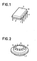
- Figure 1 shows a hybrid circuit box, seen in space, with its adaptation to withstand external pressure.
- the hybrid circuit proper is deposited on a substrate wafer 1 and is protected by a first cover 2 on one side of the substrate wafer and by a second cover 3, on the other side of the substrate wafer, the covers 2 and 3 being opposite.
- the external connections are taken by pins of a known type 4.
- the most common hybrid circuits are square or rectangular, which naturally led to the design of covers 2 and 3 which themselves have a square shape or rectangular suitable for the hybrid circuit.
- Figure 2 shows another hybrid circuit package in an attempt to find a solution to the problems of high pressures.
- This type of case is inspired by metallic power transistor cases and it consists of two half-shells 6 and 7 made of a resistant metal such as stainless steel or titanium, which half-shells are welded on their periphery.
- One of the half-shells, 6 in FIG. 2 corresponds to the base of a power transistor: it is in its central part 8 that the hybrid circuit is soldered, hidden in the figure since it is located inside the housing.
- the other half-shell, 7 in FIG. 2 corresponds to the cover of the power transistor housing.
- the electrical connections with the outside are made via output terminals which are electrically insulated and sealed in the half-shell 6 by means of glass beads.
- this adaptation of a known housing has the industrial disadvantage of requiring machining of the half-shells, polishing of the surfaces in contact for welding and to be made in materials and by means of expensive processes, which makes it, in many cases, prohibitively expensive.
- FIG. 3 represents a view in space of the hybrid circuit encapsulation box according to the invention.
- the hybrid circuit which is intended to operate under high pressures, is produced on a substrate wafer 10 conforming to the rules of the art.
- the connection pads of the hybrid circuit proper are joined to the external connection pins 11 by means which will be developed later, which means use metal strips deposited on the substrate 10.
- the encapsulation box according to the invention consists , inter alia, to be attached to the two main faces of the substrate 10, two identical half-shells or covers, 13 and 14, which have a convex shape devoid of sharp angles, these covers being fixed on either side of the substrate , so that the pressure exerted on the substrate, at the joint, by one of the covers is canceled by the pressure exerted by the other cover, and so that the central part of the substrate is thus inside the housing , outside the high pressure area.
- each of the covers 13 and 14 is that which is best suited to the resistance to pressure, since all the forces are equally distributed and perpendicular. to the wall of the cover. Furthermore, the radius of the bulge of each of the covers is adapted to the pressure to be supported: this bulge can be light enough for pressures, for example of the order of 50 bars, and reach a semi-spherical shape for much higher pressures. .
- the substrate of a hybrid circuit being conventionally made of alumina or a ceramic material
- the two covers 13 and 14 are also and advantageously made of alumina or of a ceramic homogeneous with that of substrate so that the mechanical and thermal characteristics are identical.
- each of the two parts which serve as covers is adapted to the pressure to be supported: it is in any case sufficient on the edge of the covers which come into contact with the substrate 10 to allow sealing, either directly by means of an adhesive, either by means of sealing by welding, which then requires insulating joints to prevent the welding from short-circuiting between them the connection tracks 12.
- each of the covers calls for the substrate to be square.
- the square shape which is possible, is not happy, because the substrate then has four curvilinear triangles which are fragile, which is why it has been found that an octagonal shape is particularly advantageous: on the one hand , it makes it possible to fix output pins 11 on one to eight sides if necessary, these output pins being aligned on each of the sides, which corresponds to the traditional layout of the output pins.
- the octagonal shape allows easier production of the substrates which are cut, either by laser or by striping, in the form of a square, in an alumina plate, and the four corners of which are then cut again so as to give octagons. This octagonal shape is therefore industrially more interesting than a square or round shape which is difficult to produce and the octagon inscribed fairly well inside its sides, the round shape of the covers.
- Figure 4 shows an exploded view of the same hybrid circuit as that of Figure 3 in its housing resistant to high pressures.
- Figure 4 also has the advantage of showing, thanks to a half-shell 13 which is shown in cutaway, the shape of the half-shells which serve as upper and lower covers for the housing resistant to high pressures according to the invention .
- the half-shell 13 highlights on the one hand its internal concavity, which corresponds to the volume of the hybrid circuit which it is necessary to protect against pressure, and on the other hand, the thickness of the edge of this half-shell . Indeed, the thickness of each half-shell 13 and 14 has a double function in the invention.
- the sealing of the half-shells 13 and 14 on the substrate 10 is done by the edge of the half-shells and the sealing is ensured by means of a seal with a certain surface of glue, surface necessary for the glue can withstand the effect of external pressure.
- the two half-shells work in force opposition on either side of the substrate and, if they were too thin, there could be, for example following a bad bonding of two half-shells shells which are not exactly in opposition, shearing effect and breakage of the substrate.
- the adhesive tape by which they adhere to the substrate would not be sufficient to withstand the external pressure exerted on the adhesive joint.
- the metal strips conductive 12 being thin, a very small thickness of adhesive is sufficient to ensure the sealing and bonding of the half-shells on the substrate and a thickness of a few tens of microns is largely sufficient and withstands pressure tests.
- the external connection terminals 11 shown in FIGS. 3 and 4 are metal pins of a known model frequent in hybrid circuits. However, they are outside the realm of the invention and they can be replaced by any other system suitable for the use requested for the hybrid circuit such as a wire connection directly welded to the metal strips 12, or by a taken by multiple connector.
- FIG. 4 shows only a single hybrid circuit mounted on one face of the substrate 10. However, if the number of external connections allows it and if necessary, two hybrid circuits can be mounted respectively on each of the faces of the substrate, and the external pins are shared between those which are joined to a first hybrid circuit on a first face of the substrate, by means of a certain number of metal strips J2 on this first face of the substrate and those which are joined to a second hybrid circuit on the second face of the substrate by means of other metal strips 12 situated on the other face of the substrate.
Landscapes
- Casings For Electric Apparatus (AREA)
Applications Claiming Priority (2)
| Application Number | Priority Date | Filing Date | Title |
|---|---|---|---|
| FR8013596A FR2485262A1 (fr) | 1980-06-19 | 1980-06-19 | Boitier d'encapsulation resistant a de fortes pressions externes |
| FR8013596 | 1980-06-19 |
Publications (3)
| Publication Number | Publication Date |
|---|---|
| EP0044755A2 true EP0044755A2 (de) | 1982-01-27 |
| EP0044755A3 EP0044755A3 (en) | 1982-02-10 |
| EP0044755B1 EP0044755B1 (de) | 1984-06-13 |
Family
ID=9243259
Family Applications (1)
| Application Number | Title | Priority Date | Filing Date |
|---|---|---|---|
| EP81400904A Expired EP0044755B1 (de) | 1980-06-19 | 1981-06-05 | Gegen hohe auswendige Drucke widerstandsfähiges Verkapselungsgehäuse für hybride Schaltung |
Country Status (4)
| Country | Link |
|---|---|
| US (1) | US4518818A (de) |
| EP (1) | EP0044755B1 (de) |
| DE (1) | DE3164131D1 (de) |
| FR (1) | FR2485262A1 (de) |
Families Citing this family (15)
| Publication number | Priority date | Publication date | Assignee | Title |
|---|---|---|---|---|
| FR2591801B1 (fr) * | 1985-12-17 | 1988-10-14 | Inf Milit Spatiale Aeronaut | Boitier d'encapsulation d'un circuit electronique |
| FR2688629A1 (fr) * | 1992-03-10 | 1993-09-17 | Thomson Csf | Procede et dispositif d'encapsulation en trois dimensions de pastilles semi-conductrices. |
| FR2709020B1 (fr) * | 1993-08-13 | 1995-09-08 | Thomson Csf | Procédé d'interconnexion de pastilles semi-conductrices en trois dimensions, et composant en résultant. |
| FR2719967B1 (fr) * | 1994-05-10 | 1996-06-07 | Thomson Csf | Interconnexion en trois dimensions de boîtiers de composants électroniques utilisant des circuits imprimés. |
| FR2802706B1 (fr) * | 1999-12-15 | 2002-03-01 | 3D Plus Sa | Procede et dispositif d'interconnexion en trois dimensions de composants electroniques |
| FR2832136B1 (fr) * | 2001-11-09 | 2005-02-18 | 3D Plus Sa | Dispositif d'encapsulation hermetique de composant devant etre protege de toute contrainte |
| FR2875672B1 (fr) * | 2004-09-21 | 2007-05-11 | 3D Plus Sa Sa | Dispositif electronique avec repartiteur de chaleur integre |
| FR2884049B1 (fr) * | 2005-04-01 | 2007-06-22 | 3D Plus Sa Sa | Module electronique de faible epaisseur comprenant un empilement de boitiers electroniques a billes de connexion |
| FR2894070B1 (fr) * | 2005-11-30 | 2008-04-11 | 3D Plus Sa Sa | Module electronique 3d |
| FR2895568B1 (fr) * | 2005-12-23 | 2008-02-08 | 3D Plus Sa Sa | Procede de fabrication collective de modules electroniques 3d |
| FR2905198B1 (fr) * | 2006-08-22 | 2008-10-17 | 3D Plus Sa Sa | Procede de fabrication collective de modules electroniques 3d |
| FR2911995B1 (fr) * | 2007-01-30 | 2009-03-06 | 3D Plus Sa Sa | Procede d'interconnexion de tranches electroniques |
| FR2923081B1 (fr) * | 2007-10-26 | 2009-12-11 | 3D Plus | Procede d'interconnexion verticale de modules electroniques 3d par des vias. |
| FR2940521B1 (fr) | 2008-12-19 | 2011-11-11 | 3D Plus | Procede de fabrication collective de modules electroniques pour montage en surface |
| FR2943176B1 (fr) | 2009-03-10 | 2011-08-05 | 3D Plus | Procede de positionnement des puces lors de la fabrication d'une plaque reconstituee |
Family Cites Families (6)
| Publication number | Priority date | Publication date | Assignee | Title |
|---|---|---|---|---|
| US3404215A (en) * | 1966-04-14 | 1968-10-01 | Sprague Electric Co | Hermetically sealed electronic module |
| US3436775A (en) * | 1966-12-28 | 1969-04-08 | Arthur J Schlosser | Deep submersible instrumentation package assembly |
| US3450082A (en) * | 1968-01-29 | 1969-06-17 | Ppg Industries Inc | Load-bearing member for curved ceramic segments subjected to high compressive loads |
| DE1764263A1 (de) * | 1968-05-06 | 1971-06-16 | Siemens Ag | Gut waermeableitendes Flachgehaeuse fuer Halbleitersysteme |
| CA1032276A (en) * | 1973-12-03 | 1978-05-30 | Andrew Koutalides | Package for semiconductor beam lead devices |
| US4208698A (en) * | 1977-10-26 | 1980-06-17 | Ilc Data Device Corporation | Novel hybrid packaging scheme for high density component circuits |
-
1980
- 1980-06-19 FR FR8013596A patent/FR2485262A1/fr active Granted
-
1981
- 1981-06-05 EP EP81400904A patent/EP0044755B1/de not_active Expired
- 1981-06-05 DE DE8181400904T patent/DE3164131D1/de not_active Expired
-
1984
- 1984-01-04 US US06/557,256 patent/US4518818A/en not_active Expired - Lifetime
Also Published As
| Publication number | Publication date |
|---|---|
| FR2485262A1 (fr) | 1981-12-24 |
| US4518818A (en) | 1985-05-21 |
| DE3164131D1 (en) | 1984-07-19 |
| EP0044755A3 (en) | 1982-02-10 |
| EP0044755B1 (de) | 1984-06-13 |
| FR2485262B1 (de) | 1984-10-26 |
Similar Documents
| Publication | Publication Date | Title |
|---|---|---|
| EP0044755B1 (de) | Gegen hohe auswendige Drucke widerstandsfähiges Verkapselungsgehäuse für hybride Schaltung | |
| EP0321340B1 (de) | Halter für elektronische Komponenten, insbesondere für Speicherkarten und auf solche Weise hergestelltes Produkt | |
| EP0310463A1 (de) | Gehäuse für einen hochintegrierten Schaltkreis | |
| FR2518811A1 (fr) | Dispositif a circuit integre en conteneur de ceramique | |
| FR2700416A1 (fr) | Dispositif à semiconducteurs comportant un élément semiconducteur sur un élément de montage. | |
| FR2563049A1 (fr) | Boitier pour circuit integre | |
| CH632870A5 (fr) | Boitier plat contenant un dispositif a circuits integres. | |
| EP1093159A1 (de) | Verfahren zum Einkapseln von elektronischen Komponenten | |
| EP1586122B1 (de) | Photovoltaisches modul mit aussenanschlussklemmen | |
| FR2720190A1 (fr) | Procédé de raccordement des plages de sortie d'une puce à circuit intégré, et module multipuces ainsi obtenu. | |
| CN101175978B (zh) | 红外线传感器及其制造方法 | |
| EP0226480A1 (de) | Verfahren zur Herstellung eines Mikrogehäuses mit Kontaktflecken und dessen Anwendung für Karten mit elektronischen Bauelementen | |
| EP1792526B1 (de) | Mit integriertem wärmeverteiler ausgestattete elektronische einrichtung | |
| FR2849346A1 (fr) | Boitier hyperfrequence a montage de surface et montage correspondant avec un circuit multicouche. | |
| EP0336859A1 (de) | Piezoelektrische Kapsel mit lateralen elektrischen Verbindungszangen | |
| FR3085576A1 (fr) | Couvercle pour boitier de circuit integre | |
| FR2495837A1 (fr) | Embase de microboitier d'encapsulation et microboitier comportant une telle embase | |
| EP0334747A1 (de) | Vorrichtung zur Verbindung und für den Schutz eines unbedeckten Chips eines Hochfrequenzbauteils | |
| EP3368865B1 (de) | Vorrichtung zur messung der eigenschaften einer flüssigkeit | |
| EP0079265A1 (de) | Verfahren zum Herstellen eines Sockels zum Montieren eines Halbleiterchips auf die Basis eines Verkapselungsgehäuses | |
| EP0778666A1 (de) | Piezoelektrischer Resonator | |
| FR2789822A1 (fr) | Dispositif a ondes de surface connecte a une embase avec un adhesif conducteur | |
| FR2620275A1 (fr) | Boitier pour le montage en surface d'un composant fonctionnant en hyperfrequences | |
| FR2758908A1 (fr) | Boitier d'encapsulation hyperfrequences bas cout | |
| EP0484853A1 (de) | Verfahren zum Schützen der elektronischen Bausteine einer Schaltung gegen die Strahlungen und Vorrichtung nach dem Verfahren |
Legal Events
| Date | Code | Title | Description |
|---|---|---|---|
| PUAI | Public reference made under article 153(3) epc to a published international application that has entered the european phase |
Free format text: ORIGINAL CODE: 0009012 |
|
| PUAL | Search report despatched |
Free format text: ORIGINAL CODE: 0009013 |
|
| AK | Designated contracting states |
Designated state(s): DE GB IT SE |
|
| AK | Designated contracting states |
Designated state(s): DE GB IT SE |
|
| 17P | Request for examination filed |
Effective date: 19820222 |
|
| ITF | It: translation for a ep patent filed | ||
| GRAA | (expected) grant |
Free format text: ORIGINAL CODE: 0009210 |
|
| AK | Designated contracting states |
Designated state(s): DE GB IT SE |
|
| REF | Corresponds to: |
Ref document number: 3164131 Country of ref document: DE Date of ref document: 19840719 |
|
| PLBE | No opposition filed within time limit |
Free format text: ORIGINAL CODE: 0009261 |
|
| STAA | Information on the status of an ep patent application or granted ep patent |
Free format text: STATUS: NO OPPOSITION FILED WITHIN TIME LIMIT |
|
| 26N | No opposition filed | ||
| ITTA | It: last paid annual fee | ||
| EAL | Se: european patent in force in sweden |
Ref document number: 81400904.9 |
|
| PGFP | Annual fee paid to national office [announced via postgrant information from national office to epo] |
Ref country code: GB Payment date: 19970521 Year of fee payment: 17 |
|
| PGFP | Annual fee paid to national office [announced via postgrant information from national office to epo] |
Ref country code: DE Payment date: 19970522 Year of fee payment: 17 |
|
| PGFP | Annual fee paid to national office [announced via postgrant information from national office to epo] |
Ref country code: SE Payment date: 19970523 Year of fee payment: 17 |
|
| PG25 | Lapsed in a contracting state [announced via postgrant information from national office to epo] |
Ref country code: GB Free format text: LAPSE BECAUSE OF NON-PAYMENT OF DUE FEES Effective date: 19980605 |
|
| PG25 | Lapsed in a contracting state [announced via postgrant information from national office to epo] |
Ref country code: SE Free format text: LAPSE BECAUSE OF NON-PAYMENT OF DUE FEES Effective date: 19980606 |
|
| GBPC | Gb: european patent ceased through non-payment of renewal fee |
Effective date: 19980605 |
|
| EUG | Se: european patent has lapsed |
Ref document number: 81400904.9 |
|
| PG25 | Lapsed in a contracting state [announced via postgrant information from national office to epo] |
Ref country code: DE Free format text: LAPSE BECAUSE OF NON-PAYMENT OF DUE FEES Effective date: 19990401 |