EP0334747A1 - Vorrichtung zur Verbindung und für den Schutz eines unbedeckten Chips eines Hochfrequenzbauteils - Google Patents
Vorrichtung zur Verbindung und für den Schutz eines unbedeckten Chips eines Hochfrequenzbauteils Download PDFInfo
- Publication number
- EP0334747A1 EP0334747A1 EP89400787A EP89400787A EP0334747A1 EP 0334747 A1 EP0334747 A1 EP 0334747A1 EP 89400787 A EP89400787 A EP 89400787A EP 89400787 A EP89400787 A EP 89400787A EP 0334747 A1 EP0334747 A1 EP 0334747A1
- Authority
- EP
- European Patent Office
- Prior art keywords
- substrate
- face
- interconnection
- microwave
- circuit
- Prior art date
- Legal status (The legal status is an assumption and is not a legal conclusion. Google has not performed a legal analysis and makes no representation as to the accuracy of the status listed.)
- Withdrawn
Links
Images
Classifications
-
- H—ELECTRICITY
- H10—SEMICONDUCTOR DEVICES; ELECTRIC SOLID-STATE DEVICES NOT OTHERWISE PROVIDED FOR
- H10W—GENERIC PACKAGES, INTERCONNECTIONS, CONNECTORS OR OTHER CONSTRUCTIONAL DETAILS OF DEVICES COVERED BY CLASS H10
- H10W70/00—Package substrates; Interposers; Redistribution layers [RDL]
- H10W70/60—Insulating or insulated package substrates; Interposers; Redistribution layers
- H10W70/62—Insulating or insulated package substrates; Interposers; Redistribution layers characterised by their interconnections
- H10W70/63—Vias, e.g. via plugs
- H10W70/635—Through-vias
-
- H—ELECTRICITY
- H10—SEMICONDUCTOR DEVICES; ELECTRIC SOLID-STATE DEVICES NOT OTHERWISE PROVIDED FOR
- H10W—GENERIC PACKAGES, INTERCONNECTIONS, CONNECTORS OR OTHER CONSTRUCTIONAL DETAILS OF DEVICES COVERED BY CLASS H10
- H10W44/00—Electrical arrangements for controlling or matching impedance
- H10W44/20—Electrical arrangements for controlling or matching impedance at high-frequency [HF] or radio frequency [RF]
-
- H—ELECTRICITY
- H10—SEMICONDUCTOR DEVICES; ELECTRIC SOLID-STATE DEVICES NOT OTHERWISE PROVIDED FOR
- H10W—GENERIC PACKAGES, INTERCONNECTIONS, CONNECTORS OR OTHER CONSTRUCTIONAL DETAILS OF DEVICES COVERED BY CLASS H10
- H10W72/00—Interconnections or connectors in packages
- H10W72/50—Bond wires
- H10W72/531—Shapes of wire connectors
- H10W72/533—Cross-sectional shape
- H10W72/534—Cross-sectional shape being rectangular
-
- H—ELECTRICITY
- H10—SEMICONDUCTOR DEVICES; ELECTRIC SOLID-STATE DEVICES NOT OTHERWISE PROVIDED FOR
- H10W—GENERIC PACKAGES, INTERCONNECTIONS, CONNECTORS OR OTHER CONSTRUCTIONAL DETAILS OF DEVICES COVERED BY CLASS H10
- H10W72/00—Interconnections or connectors in packages
- H10W72/50—Bond wires
- H10W72/551—Materials of bond wires
- H10W72/552—Materials of bond wires comprising metals or metalloids, e.g. silver
-
- H—ELECTRICITY
- H10—SEMICONDUCTOR DEVICES; ELECTRIC SOLID-STATE DEVICES NOT OTHERWISE PROVIDED FOR
- H10W—GENERIC PACKAGES, INTERCONNECTIONS, CONNECTORS OR OTHER CONSTRUCTIONAL DETAILS OF DEVICES COVERED BY CLASS H10
- H10W90/00—Package configurations
- H10W90/701—Package configurations characterised by the relative positions of pads or connectors relative to package parts
- H10W90/751—Package configurations characterised by the relative positions of pads or connectors relative to package parts of bond wires
- H10W90/754—Package configurations characterised by the relative positions of pads or connectors relative to package parts of bond wires between a chip and a stacked insulating package substrate, interposer or RDL
Definitions
- the present invention relates to an interconnection and protection device for a microwave integrated circuit chip made of III-V materials, such as GaAs.
- a microwave integrated circuit mounted in this device does not see its performance reduced by the device, in a frequency range from continuous to at least 40 GHz, and 60 GHz if the substrate is suitable.
- MMIC Microwave Monolithic Integrated Circuit
- these integrated circuits are very generally made of GaAs, or comparable materials such as AlGaAs, InP, etc., whose surface protection Si3 N4 is not optimal, as for a silicon circuit. It is therefore necessary to protect them from climatic-mechanical constraints by an encapsulation box.
- an MMIC which functions well in the state of a bare chip sees its characteristics greatly degraded when it is encapsulated in a case.
- Many parameters are involved, including the volume of the housing cavity and the passage of access connections through the walls of the housing. These are either coaxial connections, made of glass pearls, which is illogical since the circuit associated with an MMIC is very generally in microstrips, or flat connections which pass through the case, in the plane of bonding of the cover on the base, in the thickness of a layer of glass, but which has microwave leaks.
- the device according to the invention provides a solution to these environmental problems of an MMIC chip, by taking as a starting element a thin ceramic substrate which alone constitutes a part of a microstrip circuit. That is to say that this ceramic substrate supports the MMIC chip and the microstrip lines which make it possible to interconnect this element with other comparable elements - cascade mounting - or with an external circuit in microstrips.
- the MMIC chip cannot be protected by a layer of glass or a drop of polymer, it is arranged, no longer as in the known art on the face of the substrate which carries the interconnection in microstrips, and which constitutes normally the upper face of a microwave circuit, but on the contrary under this substrate, and it is protected by the fixing plate of the device, which also serves as a radiator, in which a local thinning provides a cell for housing the MMIC chip and possibly other components, such as capacitors.
- the MMIC chip, and the other possible components, are joined to the network of microstrips on the upper face by means of metallized holes, which are hermetically sealed.
- the device according to the invention essentially consists of a double-sided etched substrate, which carries on its underside at least one microwave component in bare chip, protected by the fixing soleplate in which a cell is formed, and on its upper face at least one network of microstrips and possibly components such as capacitors, inductors and chips in glassivated silicon, the two faces being interconnected by means of metallized holes blocked by solder.
- the sole is hermetically brazed on the double-sided substrate.
- the invention which has been developed more specifically for integrated circuits, also applies to microwave transistors.
- the invention relates to a device for interconnection and protection of a bare wafer of microwave semiconductor component, made of group III-V materials, characterized in that it comprises: a thin substrate of dielectric material, a first face of which supports an array of microstrip lines and a second face of which supports a ground plane metallization for the microstrip lines of the first face, at least one chip of microwave semiconductor component, fixed to the ground plane metallization of the second face of the substrate, electrically connected to the microstrip lines of the first face of the substrate by means of plugged metallized holes, - a metallic sole, in which a cell releases a housing for the semiconductor component fixed on the second face of the substrate, the ground plane metallization of which is soldered to the sole by means of a solder preform.
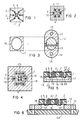
- Figures 1 and 2 show the substrate of the device of the invention. It is a ceramic plate, square or rectangular, about 5 mm side by 0.25 to 0.75 mm thick. It is preferably in alumina at 99.6% purity.
- the substrate 1 supports a network of microstrip lines 2, which run from a central range towards the periphery of the substrate.
- microstrips 2 shown in the figures in no way limits the scope of the invention: there are as many as required by the MMIC chip or transistor associated with this substrate.
- These microstrips are preferably produced by sputtering or evaporation of metal under vacuum, or by screen printing. Similarly, they can terminate on the four sides of the substrate 1, as will be seen later, but the usual microwave assemblies require that they terminate on at least two sides.
- microbands have two particularities: - they both have metallization areas 3 and 4 at their two ends, - Their "central" end with respect to the substrate 1 surrounds a hole 5 which passes through the ceramic plate.
- the metallized area 3, at the end on the periphery of the substrate 1, makes it possible to wire by conventional techniques or metallic ribbon connecting with the external circuit, in microstrip environment.
- the metallized area 4, at the "central" end with respect to the substrate 1, is pierced by a hole 5 and provides electrical contact with this metallized hole to which we will return later.
- This microstrip face also includes a central metallization area 6, connected by at least one metallized hole 7 to the other face of the substrate 1.
- the second face of the substrate 1 or lower face, in FIG. 2, is of the coplanar type: it simply comprises a metallization 8 which constitutes the ground plane for the microstrip lines 2 of the first face.
- An etching in the metallization 8 creates reserves 9 which isolate small metallization areas 10 around the holes 5.
- the holes 7 are in electrical contact with the metallization 8.
- the central area 11, on the ground plane 8, lying between the reserves 9, is of sufficient dimensions to be able to fix thereon, by solder or conductive adhesive, an MMIC chip, the substrate of which is therefore grounded to the ground plane 8.
- All of the holes 5 and 7 which pass through the ceramic substrate 1 are metallized during the metallization operation of the two faces, before etching, then are plugged with a gold-tin or gold-germanium solder paste; a reflow at an appropriate temperature according to the solder paste forms a hermetic seal in each hole.
- the circuit elements such as that described, comprising a small ceramic substrate, are most often fixed on a metal soleplate, which has a double objective: to transmit the heat released in operation, and to manipulate for the electrical measurement and to fix this microwave circuit element.
- FIG. 3 represents a plan view of the sole of the interconnection device according to the invention, and, next to it, of the solder preform of the sole.
- the metal soleplate of the device comprises at least one central part 12 whose dimensions are the same as those of the substrate 1. It has a thickness of between 0.5 and 1 mm, and, in order to be able to braze it on the ground plane 8 of the substrate 1, it has in its central part a thinning at 13, thus creating a cell of about 0.25 - 0.30 mm in depth, sufficient to accommodate the MMIC chip. In order to better show the profile of the sole, its cut is superimposed on its plane, in Figure 3.
- the sole 12 may also include, on two opposite sides, two metal end pieces 14, each pierced with a hole 15, which allow the device to be fixed on a support.
- a brazing preform 16 enables the sole 12 to be hermetically fixed to the ground plane 8 of the interconnection device.
- This preform 16 also has the same dimensions as the substrate 1, and it is perforated with a central hole 17 to make room for the MMIC chip and its connections and associated components.
- FIG. 4 A plan view, enlarged with respect to FIG. 2, shows in FIG. 4 the arrangement of the circuit on the underside of the interconnection circuit.
- At least one MMIC or transistor chip 18 is soldered on the central area 11 of the ground plane 8.
- it is connected by wires or metallic ribbons 19 to an environment circuit, which may include inductors - by the length of the wires 19 - capacities 20, or other chips of semiconductors - not shown -.
- this face of the ceramic substrate 1 comprises at least one bare chip made of III-V material and all of its environment for which the bond lengths are crucial.
- the output of this circuit is made by connection to the plugged metallized holes 5, which are in contact with the microstrip circuit on the other face of the substrate.
- the object of Figure 5 which gives a sectional view of the device according to the invention, is to highlight the double-sided appearance of the circuit.
- This chip is protected from climato-mechanical constraints by the cell hollowed out in the sole 12.
- On the upper face there is at least the network of microstrips 2 but there can also be a complementary electronic circuit, such as for example a voltage regulator chip 21 - in glassivated silicon or protected by a drop of varnish - one or more capacitances 22, or a heat radiator 23 - shown in FIG.
- the device according to the invention corresponds to the case where the sole is limited to its central part 12, without the end caps 14.
- This device can be glued or brazed to a support.
- the double-sided circuit ensures the interconnection of the MMIC, and the sole provides protection: it is not, however, an encapsulation box.
- the cell in the sole 12 may have a thickness equal to that of the sole, which is then pierced.
- This type of device makes it possible to reach the microwave circuit of the MMIC on the underside of the substrate 1, to make measurements there, and to adjust it, for example.
- the sole is preferably fitted with end caps 14: in normal service, it will be brazed and / or screwed onto a support 24, which replaces the membrane 13 of the cell to protect the MMIC chip: the interconnection device is in this case closed on itself by the support 24, ceramic or metallic.
- FIG. 7 gives an exploded view in space of an interconnection device according to the invention.
- the upper face of the substrate 1 is shown there intentionally devoid of any component other than the microstrips 2, with their areas 3 and 4, and the plugged metallized holes 5 and 7: this in order not to introduce confusion, since the integrated circuit MMIC 18 - shown in dotted lines - and its immediate environment are placed on the underside of the substrate 1.
- the upper face of this interconnection circuit may also include, near the microstrips 2, small metallized studs 25 which are used, as is known, to adjust the line impedance. This is also defined, according to known laws, by the width of a microstrip line 2 and by the thickness and the dielectric constant of the substrate 1. It is therefore possible, by playing on these three data, to obtain a interconnection network whose line impedances are perfectly adapted to the frequency.
- the device according to the invention achieves the following performances: - transmission losses: 1 dB from 0 to 40 GHz - losses by reflection: ⁇ 10 dB from 0 to 40 GHz, these two values including the losses in transmission and by reflection of the measurement assembly, - isolation between each pair of microstrips:> 30 dB from 0 to 20 GHz - airtightness: 10-7 atm./cm3/s for helium, for a circuit in which the sole is dimpled.
- the interconnection network being of microstrip type is perfectly suited to a microstrip environment, without passing through coaxial connectors, and it is cascadable, as shown in Figures 8 and 9.
- the first interconnection circuit is provided on its upper face with a voltage regulator circuit 21, which supplies in parallel the MMICs 18 fixed on the lower faces of the substrates, double face, and the two following interconnection circuits are each provided with a heat sink 23.
- a voltage regulator circuit 21 which supplies in parallel the MMICs 18 fixed on the lower faces of the substrates, double face, and the two following interconnection circuits are each provided with a heat sink 23.
- the interconnection and protection device for a bare chip of microwave component is used for amplifiers, oscillators or other microwave circuits, in a range between 0 and 60 GHz.
Landscapes
- Waveguides (AREA)
- Microwave Amplifiers (AREA)
- Junction Field-Effect Transistors (AREA)
Applications Claiming Priority (2)
| Application Number | Priority Date | Filing Date | Title |
|---|---|---|---|
| FR8803950 | 1988-03-25 | ||
| FR8803950A FR2629271B1 (fr) | 1988-03-25 | 1988-03-25 | Dispositif d'interconnexion et de protection d'une pastille nue de composant hyperfrequence |
Publications (1)
| Publication Number | Publication Date |
|---|---|
| EP0334747A1 true EP0334747A1 (de) | 1989-09-27 |
Family
ID=9364652
Family Applications (1)
| Application Number | Title | Priority Date | Filing Date |
|---|---|---|---|
| EP89400787A Withdrawn EP0334747A1 (de) | 1988-03-25 | 1989-03-21 | Vorrichtung zur Verbindung und für den Schutz eines unbedeckten Chips eines Hochfrequenzbauteils |
Country Status (5)
| Country | Link |
|---|---|
| US (1) | US4996588A (de) |
| EP (1) | EP0334747A1 (de) |
| JP (1) | JPH0210756A (de) |
| CA (1) | CA1301949C (de) |
| FR (1) | FR2629271B1 (de) |
Cited By (5)
| Publication number | Priority date | Publication date | Assignee | Title |
|---|---|---|---|---|
| EP0446125A1 (de) * | 1990-03-09 | 1991-09-11 | Thomson-Csf Semiconducteurs Specifiques | Leistungshalbleiteranordnung |
| EP0438056A3 (en) * | 1990-01-17 | 1991-12-11 | Sony Corporation | High-frequency circuit package |
| EP0527468A1 (de) * | 1991-08-12 | 1993-02-17 | Hitachi, Ltd. | Hochfrequenzmodul |
| US5319237A (en) * | 1990-03-09 | 1994-06-07 | Thomson Composants Microondes | Power semiconductor component |
| FR2699330A1 (fr) * | 1992-12-11 | 1994-06-17 | Mitsubishi Electric Corp | Boîtier pour circuit intégré à haute fréquence. |
Families Citing this family (5)
| Publication number | Priority date | Publication date | Assignee | Title |
|---|---|---|---|---|
| US6261872B1 (en) * | 1997-09-18 | 2001-07-17 | Trw Inc. | Method of producing an advanced RF electronic package |
| US5945897A (en) * | 1998-04-30 | 1999-08-31 | Lockheed Martin Corporation | Compliant RF coaxial interconnect |
| US6081988A (en) * | 1998-04-30 | 2000-07-04 | Lockheed Martin Corp. | Fabrication of a circuit module with a coaxial transmission line |
| US6031188A (en) * | 1998-04-30 | 2000-02-29 | Lockheed Martin Corp. | Multi-circuit RF connections using molded and compliant RF coaxial interconnects |
| WO2012135406A2 (en) * | 2011-04-01 | 2012-10-04 | Schlumberger Canada Limited | High density microelectronics packaging |
Citations (4)
| Publication number | Priority date | Publication date | Assignee | Title |
|---|---|---|---|---|
| US4276558A (en) * | 1979-06-15 | 1981-06-30 | Ford Aerospace & Communications Corp. | Hermetically sealed active microwave integrated circuit |
| FR2507409A1 (fr) * | 1981-06-03 | 1982-12-10 | Radiotechnique Compelec | Circuit hyperfrequence, notamment amplificateur a transistor a effet de champ |
| EP0177943A2 (de) * | 1984-10-08 | 1986-04-16 | Fujitsu Limited | Packung für Hochfrequenzhalbleiterbauelemente |
| EP0187580A1 (de) * | 1984-12-11 | 1986-07-16 | Thomson-Csf | Gehäuse für ein mit einem Wasserumlauf gekühltes Hochfrequenzleistungselement |
Family Cites Families (8)
| Publication number | Priority date | Publication date | Assignee | Title |
|---|---|---|---|---|
| US3290564A (en) * | 1963-02-26 | 1966-12-06 | Texas Instruments Inc | Semiconductor device |
| US3927815A (en) * | 1971-11-22 | 1975-12-23 | Ngk Insulators Ltd | Method for producing multilayer metallized beryllia ceramics |
| JPS55166941A (en) * | 1979-06-13 | 1980-12-26 | Nec Corp | Semiconductor device |
| US4423468A (en) * | 1980-10-01 | 1983-12-27 | Motorola, Inc. | Dual electronic component assembly |
| JPS5756953A (en) * | 1981-08-10 | 1982-04-05 | Nec Corp | Transistor |
| JPS58182250A (ja) * | 1982-04-16 | 1983-10-25 | Mitsubishi Electric Corp | 半導体装置 |
| JPS6189653A (ja) * | 1984-10-09 | 1986-05-07 | Fujitsu Ltd | リ−ドピンの装着方法 |
| JPS62269349A (ja) * | 1986-05-19 | 1987-11-21 | Nec Corp | 半導体装置 |
-
1988
- 1988-03-25 FR FR8803950A patent/FR2629271B1/fr not_active Expired - Fee Related
-
1989
- 1989-03-21 EP EP89400787A patent/EP0334747A1/de not_active Withdrawn
- 1989-03-21 US US07/326,646 patent/US4996588A/en not_active Expired - Fee Related
- 1989-03-23 CA CA000594548A patent/CA1301949C/en not_active Expired - Fee Related
- 1989-03-27 JP JP1072019A patent/JPH0210756A/ja active Pending
Patent Citations (4)
| Publication number | Priority date | Publication date | Assignee | Title |
|---|---|---|---|---|
| US4276558A (en) * | 1979-06-15 | 1981-06-30 | Ford Aerospace & Communications Corp. | Hermetically sealed active microwave integrated circuit |
| FR2507409A1 (fr) * | 1981-06-03 | 1982-12-10 | Radiotechnique Compelec | Circuit hyperfrequence, notamment amplificateur a transistor a effet de champ |
| EP0177943A2 (de) * | 1984-10-08 | 1986-04-16 | Fujitsu Limited | Packung für Hochfrequenzhalbleiterbauelemente |
| EP0187580A1 (de) * | 1984-12-11 | 1986-07-16 | Thomson-Csf | Gehäuse für ein mit einem Wasserumlauf gekühltes Hochfrequenzleistungselement |
Non-Patent Citations (3)
| Title |
|---|
| PATENT ABSTRACTS OF JAPAN, vol. 5, no. 44 (E-50)[716], 24 mars 1981, page 96 E 50; & JP-A-55 166 941 (NIPPON DENKI K.K.) 26-12-1980 * |
| PATENT ABSTRACTS OF JAPAN, vol. 5, no. 8 (E-223)[1454], 25 janvier 1984, page 148 E 223; & JP-A-58 182 251 (MITSUBISHI DENKI K.K.) 25-10-1983 * |
| PATENT ABSTRACTS OF JAPAN, vol. 6, no. 132 (E-119)[1010], 17 juillet 1982, page 15 E 119; & JP-A-57 056 953 (NIPPON DENKI K.K.) 05-04-1982 * |
Cited By (7)
| Publication number | Priority date | Publication date | Assignee | Title |
|---|---|---|---|---|
| EP0438056A3 (en) * | 1990-01-17 | 1991-12-11 | Sony Corporation | High-frequency circuit package |
| EP0446125A1 (de) * | 1990-03-09 | 1991-09-11 | Thomson-Csf Semiconducteurs Specifiques | Leistungshalbleiteranordnung |
| FR2659494A1 (fr) * | 1990-03-09 | 1991-09-13 | Thomson Composants Microondes | Composant semiconducteur de puissance, dont la puce est montee a l'envers. |
| US5319237A (en) * | 1990-03-09 | 1994-06-07 | Thomson Composants Microondes | Power semiconductor component |
| EP0527468A1 (de) * | 1991-08-12 | 1993-02-17 | Hitachi, Ltd. | Hochfrequenzmodul |
| US5438305A (en) * | 1991-08-12 | 1995-08-01 | Hitachi, Ltd. | High frequency module including a flexible substrate |
| FR2699330A1 (fr) * | 1992-12-11 | 1994-06-17 | Mitsubishi Electric Corp | Boîtier pour circuit intégré à haute fréquence. |
Also Published As
| Publication number | Publication date |
|---|---|
| US4996588A (en) | 1991-02-26 |
| CA1301949C (en) | 1992-05-26 |
| JPH0210756A (ja) | 1990-01-16 |
| FR2629271B1 (fr) | 1991-03-29 |
| FR2629271A1 (fr) | 1989-09-29 |
Similar Documents
| Publication | Publication Date | Title |
|---|---|---|
| EP0113273B1 (de) | Verkapselungsgehäuse für Leistungshalbleiter mit Eingangs-/Ausgangs-Isolierung | |
| EP0228953B1 (de) | Verkapselungsgehäuse für eine elektronische Schaltung | |
| EP0310463A1 (de) | Gehäuse für einen hochintegrierten Schaltkreis | |
| EP0133125A1 (de) | Gehäuse für einen elektronischen Baustein mit einem Kondensator | |
| FR2665574A1 (fr) | Procede d'interconnexion entre un circuit integre et un circuit support, et circuit integre adapte a ce procede. | |
| EP0334747A1 (de) | Vorrichtung zur Verbindung und für den Schutz eines unbedeckten Chips eines Hochfrequenzbauteils | |
| FR2645681A1 (fr) | Dispositif d'interconnexion verticale de pastilles de circuits integres et son procede de fabrication | |
| EP1573809A1 (de) | An der oberfläche angebrachte mikrowellenkapselung und entsprechende anbringung mit mehrschichtiger schaltung | |
| WO2006067045A1 (fr) | Boitier miniature hyperfrequence et procede de fabrication du boitier | |
| EP0387955A1 (de) | Gehäuse für eine integrierte Hyperfrequenzschaltung | |
| EP0044755A2 (de) | Gegen hohe auswendige Drucke widerstandsfähiges Verkapselungsgehäuse für hybride Schaltung | |
| EP0079265B1 (de) | Verfahren zum Herstellen eines Sockels zum Montieren eines Halbleiterchips auf die Basis eines Verkapselungsgehäuses | |
| FR2693031A1 (fr) | Dispositif à semiconducteurs, substrat et cadre de montage pour ce dispositif. | |
| FR2565030A1 (fr) | Structure de metallisations de reprise de contacts d'un dispositif semi-conducteur et dispositif dote d'une telle structure | |
| FR2618944A1 (fr) | Dispositif a semi-conducteur encapsule dans un boitier comprenant un support metallique et un corps en resine synthetique | |
| EP0101335A1 (de) | Mikrogehaüse-Verkapselung für logische integrierte Schaltungen, funktionierend bei sehr hoher Frequenz | |
| FR2847726A1 (fr) | Module radiofrequence | |
| EP1657749B1 (de) | Mehrlagiges Mikroelektronik-Gehäuse mit interner Abschirmung | |
| FR2620275A1 (fr) | Boitier pour le montage en surface d'un composant fonctionnant en hyperfrequences | |
| EP0158550A1 (de) | Hyperfrequenz-Halbleiteranordnung mit äusseren Balkenleiter-Verbindungen | |
| EP0983616B1 (de) | Verfahren und vorrichtung zum verbinden zweier millimeterelemente | |
| EP0962980B1 (de) | Mikroelektronisches Hyperfrequenzmodul mit zwei verschiedenen Substratmaterialen und Herstellungsverfahren eines solchen Moduls | |
| FR2874127A1 (fr) | Boitier miniature hyperfrequence pour montage en surface et procede de fabrication du boitier | |
| FR2758417A1 (fr) | Boitier d'encapsulation de composant hyperfrequence, et procede d'obtention | |
| FR2745119A1 (fr) | Boitier d'encapsulation de circuit integre pour applications hyperfrequences et son procede de fabrication |
Legal Events
| Date | Code | Title | Description |
|---|---|---|---|
| PUAI | Public reference made under article 153(3) epc to a published international application that has entered the european phase |
Free format text: ORIGINAL CODE: 0009012 |
|
| AK | Designated contracting states |
Kind code of ref document: A1 Designated state(s): DE GB IT NL SE |
|
| 17P | Request for examination filed |
Effective date: 19891019 |
|
| 17Q | First examination report despatched |
Effective date: 19910705 |
|
| STAA | Information on the status of an ep patent application or granted ep patent |
Free format text: STATUS: THE APPLICATION IS DEEMED TO BE WITHDRAWN |
|
| 18D | Application deemed to be withdrawn |
Effective date: 19920825 |