EP0045561A2 - Dispositif semiconducteur comprenant des circuits à mémoire - Google Patents
Dispositif semiconducteur comprenant des circuits à mémoire Download PDFInfo
- Publication number
- EP0045561A2 EP0045561A2 EP81302676A EP81302676A EP0045561A2 EP 0045561 A2 EP0045561 A2 EP 0045561A2 EP 81302676 A EP81302676 A EP 81302676A EP 81302676 A EP81302676 A EP 81302676A EP 0045561 A2 EP0045561 A2 EP 0045561A2
- Authority
- EP
- European Patent Office
- Prior art keywords
- semiconductor device
- resinous film
- memory cells
- resinous
- substrate
- Prior art date
- Legal status (The legal status is an assumption and is not a legal conclusion. Google has not performed a legal analysis and makes no representation as to the accuracy of the status listed.)
- Granted
Links
Images

Classifications
-
- H—ELECTRICITY
- H10—SEMICONDUCTOR DEVICES; ELECTRIC SOLID-STATE DEVICES NOT OTHERWISE PROVIDED FOR
- H10W—GENERIC PACKAGES, INTERCONNECTIONS, CONNECTORS OR OTHER CONSTRUCTIONAL DETAILS OF DEVICES COVERED BY CLASS H10
- H10W74/00—Encapsulations, e.g. protective coatings
- H10W74/10—Encapsulations, e.g. protective coatings characterised by their shape or disposition
- H10W74/131—Encapsulations, e.g. protective coatings characterised by their shape or disposition the semiconductor body being only partially enclosed
- H10W74/137—Encapsulations, e.g. protective coatings characterised by their shape or disposition the semiconductor body being only partially enclosed the encapsulations being directly on the semiconductor body
-
- H—ELECTRICITY
- H10—SEMICONDUCTOR DEVICES; ELECTRIC SOLID-STATE DEVICES NOT OTHERWISE PROVIDED FOR
- H10B—ELECTRONIC MEMORY DEVICES
- H10B12/00—Dynamic random access memory [DRAM] devices
-
- H—ELECTRICITY
- H10—SEMICONDUCTOR DEVICES; ELECTRIC SOLID-STATE DEVICES NOT OTHERWISE PROVIDED FOR
- H10W—GENERIC PACKAGES, INTERCONNECTIONS, CONNECTORS OR OTHER CONSTRUCTIONAL DETAILS OF DEVICES COVERED BY CLASS H10
- H10W42/00—Arrangements for protection of devices
- H10W42/20—Arrangements for protection of devices protecting against electromagnetic or particle radiation, e.g. light, X-rays, gamma-rays or electrons
- H10W42/25—Arrangements for protection of devices protecting against electromagnetic or particle radiation, e.g. light, X-rays, gamma-rays or electrons against alpha rays, e.g. for outer space applications
Definitions
- This invention relates to a semiconductor device, particularly a semiconductor device comprising memory circuits coated with a protective resinous film in order to eliminate soft errors by shielding radioactive rays.
- a semiconductor device, on ' which memory cells etc. are fabricated, is usually enclosed within a ceramic or plastic package. It is known that the ceramic materials are contaminated with uranium and thorium in an amount of several parts per million and the plastic package materials include ceramic fillers which are also contaminated with radioactive materials.
- the radioactive materials emit radioactive rays.
- a protective film made of a radiation shielding resin such as polyimide and silicone, is generally applied on the surface of a semiconductor chip.
- the resinous film When the energy of the emitting a-particle is assumed to be 5 MeV, the resinous film must have a thickness of from 30 to 50 pm in order to inhibit the penetration of a-particles.
- This protective film is thicker than other films applied on a semiconductor device, such as silicon oxide film, phospho-silicate glass and so on.
- the resinous material suffers from a large strain due to the contraction of its volume when it is cured on the substrate. Furthermore, the difference of thermal expansion between the protective resinous material and the substrate material, e.g., polyimide and silicon, affects mechanical strain, especially when the chip is enclosed in a ceramic package at a temperature of about 450°C. Because the coefficients of thermal expansion of polyimide, silicone and silicon are 27 x 1O -6 /°C, 50 x 10 JOC and 2.3 x 10 -6 /°C, respectively, the expansion of the coating resin is ten times larger than that of the substrate. This strain is emphasized by the thickness and coating area of the protective film.
- Japanese Patent Application Laid-open No: 55-128851 of J. Shirasu et al. discloses a semiconductor device prepared from a silicon wafer which is coated by a protective resinous film except for the bonding pads region and the scribing region.
- this patent application does not teach to divide the protective resinous film into several portions so as to decrease the area of a single coating portion and, consequently, reduce the amount of the strain caused between the protective film and the substrate.
- a semiconductor device comprising a chip of a semiconductor substrate in which memory circuits including memory cells and sense amplifiers are fabricated, characterized in that a resinous film formed on said chip for shielding radioactive rays is divided into a plurality of portions, said portions being separated from one another and coating at least said memory cells and sense amplifiers.
- a semiconductor device comprising a chip of semiconductor substrate in which memory cells and sense amplifiers are fabricated, characterized in that a resinous film is formed on said chip and coating at least said memory cells and sense amplifiers, a part of said resinous film is removed at the portion other than said memory cells and sense amplifers, whereby the strain between said resinous film and substrate becomes small.
- said resinous film is made of polyimide or silicone.
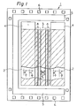
- the areas of memory cells 2 or sense amplifiers 3 are covered by individual portions of the protective resinous film (shown as hatched portions) which are separated from one another by the areas where decoders 4 are fabricated. Therefore, each portion of the resinous film which covers the region 2 or 3 has relatively small area. And the resinous film does not cover the areas where decoders 4 and peripheral circuits, such as clock generators and I/O buffers 5 and pads 6 are fabricated. ,
- portions of the resinous film may be easily formed by a usual method, such as masked screen printing and photolithography followed by etching using hydrazine N 2 H 4
- the chip sizes of the semiconductor devices are 5.3 mm x 2.8 mm and 6.5 mm x 3.4 mm, respectively.
- the sizes of individual portions of the resinous films are as small as 3.9 mm x 0.8 mm and 1.2 mm x 1.2 mm, respectively.
- the thickness of the resinous film is relatively large as 50 pm, the contraction by curing and the thermal expansion of the coating resin cause relatively small strain between the coating resinous film and the substrate and, consequently, the reliability of the semiconductor device is improved.
- the resinous film (shown as hatched portion) is not divided into a plurality of portions. But a part of the resinous film is removed at the portion 7 where circuits, such as decoders 4, other than memory cells 2 and sense amplifiers 3 are fabricated. In this embodiment, a strain between the resinous film and substrate becomes small.
- the semiconductor devices according to the present invention can inhibit the penetration of radioactive ray to irradiation sensitive members, such as memory cells and sense amplifiers, so that they do not suffer from the so-called soft errors during its operation.
Landscapes
- Structures Or Materials For Encapsulating Or Coating Semiconductor Devices Or Solid State Devices (AREA)
- Semiconductor Memories (AREA)
- Formation Of Insulating Films (AREA)
Applications Claiming Priority (2)
| Application Number | Priority Date | Filing Date | Title |
|---|---|---|---|
| JP81953/80 | 1980-06-17 | ||
| JP8195380A JPS577144A (en) | 1980-06-17 | 1980-06-17 | Semiconductor device |
Publications (3)
| Publication Number | Publication Date |
|---|---|
| EP0045561A2 true EP0045561A2 (fr) | 1982-02-10 |
| EP0045561A3 EP0045561A3 (en) | 1984-07-18 |
| EP0045561B1 EP0045561B1 (fr) | 1987-03-11 |
Family
ID=13760858
Family Applications (1)
| Application Number | Title | Priority Date | Filing Date |
|---|---|---|---|
| EP81302676A Expired EP0045561B1 (fr) | 1980-06-17 | 1981-06-16 | Dispositif semiconducteur comprenant des circuits à mémoire |
Country Status (5)
| Country | Link |
|---|---|
| US (1) | US4481526A (fr) |
| EP (1) | EP0045561B1 (fr) |
| JP (1) | JPS577144A (fr) |
| DE (1) | DE3175993D1 (fr) |
| IE (1) | IE52491B1 (fr) |
Cited By (2)
| Publication number | Priority date | Publication date | Assignee | Title |
|---|---|---|---|---|
| EP0102525A3 (en) * | 1982-08-23 | 1986-01-15 | Burroughs Corporation (A Michigan Corporation) | Alpha-particle protection in integrated circuit packages |
| EP0152334A3 (en) * | 1984-02-09 | 1986-02-05 | Fairchild Camera & Instrument Corporation | Semiconductor structure having alpha particle resistant film and method of making the same |
Families Citing this family (7)
| Publication number | Priority date | Publication date | Assignee | Title |
|---|---|---|---|---|
| US4653175A (en) * | 1984-02-09 | 1987-03-31 | Fairchild Semiconductor Corporation | Semiconductor structure having alpha particle resistant film and method of making the same |
| JPH0697555B2 (ja) * | 1985-05-27 | 1994-11-30 | 株式会社日立製作所 | 磁気バブルメモリ |
| JPH02234085A (ja) * | 1989-03-08 | 1990-09-17 | Mitsubishi Electric Corp | 半導体装置 |
| US5187558A (en) * | 1989-05-08 | 1993-02-16 | Mitsubishi Denki Kabushiki Kaisha | Stress reduction structure for a resin sealed semiconductor device |
| US8159043B2 (en) | 2004-03-12 | 2012-04-17 | Semiconductor Energy Laboratory Co., Ltd. | Semiconductor device |
| CN101101882A (zh) * | 2006-07-05 | 2008-01-09 | 阎跃军 | 基板树脂封装方法 |
| US10109609B2 (en) | 2014-01-13 | 2018-10-23 | Infineon Technologies Austria Ag | Connection structure and electronic component |
Family Cites Families (3)
| Publication number | Priority date | Publication date | Assignee | Title |
|---|---|---|---|---|
| JPS5568659A (en) * | 1978-11-20 | 1980-05-23 | Hitachi Ltd | Semiconductor device and manufacturing method thereof |
| JPS55128851A (en) * | 1979-03-28 | 1980-10-06 | Hitachi Ltd | Semiconductor memory device |
| JPS6015152B2 (ja) * | 1980-01-09 | 1985-04-17 | 株式会社日立製作所 | 樹脂封止半導体メモリ装置 |
-
1980
- 1980-06-17 JP JP8195380A patent/JPS577144A/ja active Pending
-
1981
- 1981-06-16 EP EP81302676A patent/EP0045561B1/fr not_active Expired
- 1981-06-16 DE DE8181302676T patent/DE3175993D1/de not_active Expired
- 1981-06-16 IE IE1337/81A patent/IE52491B1/en not_active IP Right Cessation
- 1981-06-17 US US06/274,542 patent/US4481526A/en not_active Expired - Fee Related
Cited By (2)
| Publication number | Priority date | Publication date | Assignee | Title |
|---|---|---|---|---|
| EP0102525A3 (en) * | 1982-08-23 | 1986-01-15 | Burroughs Corporation (A Michigan Corporation) | Alpha-particle protection in integrated circuit packages |
| EP0152334A3 (en) * | 1984-02-09 | 1986-02-05 | Fairchild Camera & Instrument Corporation | Semiconductor structure having alpha particle resistant film and method of making the same |
Also Published As
| Publication number | Publication date |
|---|---|
| EP0045561A3 (en) | 1984-07-18 |
| IE811337L (en) | 1981-12-17 |
| EP0045561B1 (fr) | 1987-03-11 |
| IE52491B1 (en) | 1987-11-25 |
| JPS577144A (en) | 1982-01-14 |
| US4481526A (en) | 1984-11-06 |
| DE3175993D1 (en) | 1987-04-16 |
Similar Documents
| Publication | Publication Date | Title |
|---|---|---|
| US4541003A (en) | Semiconductor device including an alpha-particle shield | |
| FR2473772B1 (fr) | Dispositif de memoire a semi-conducteurs et procede pour le fabriquer | |
| EP0045561B1 (fr) | Dispositif semiconducteur comprenant des circuits à mémoire | |
| JP2000195891A (ja) | 半導体素子の製造方法 | |
| EP0029858B1 (fr) | Dispositif a semi-conducteur | |
| US4423548A (en) | Method for protecting a semiconductor device from radiation indirect failures | |
| EP0021643B1 (fr) | Dispositif semiconducteur comprenant une structure préventive contre une erreur du type "soft-error" | |
| US5264726A (en) | Chip-carrier | |
| JPS60106150A (ja) | 耐放射線パツケ−ジ | |
| JPS5636136A (en) | Semiconductor device | |
| CA2021682C (fr) | Porte-puce avec ecran contre les rayons alpha | |
| JPS58107657A (ja) | 半導体装置 | |
| JP2837488B2 (ja) | 半導体装置 | |
| EP0028490B1 (fr) | Circuit intégré comportant des moyens de protection contre les rayonnements alpha | |
| JPS6136709B2 (fr) | ||
| JP2576496B2 (ja) | 半導体記憶装置 | |
| JP3087158B2 (ja) | 半導体装置 | |
| JPS6054444A (ja) | 半導体装置の製造方法 | |
| JPS5817642A (ja) | 半導体デバイス用保護装置 | |
| JPS5736847A (en) | Semiconductor integrated circuit mounting device | |
| JP2836165B2 (ja) | チツプキヤリア | |
| JPS6138861B2 (fr) | ||
| JPS5891663A (ja) | 半導体装置およびその製造方法 | |
| KR100192434B1 (ko) | 반도체 소자의 제조방법 | |
| JPS6332267B2 (fr) |
Legal Events
| Date | Code | Title | Description |
|---|---|---|---|
| PUAI | Public reference made under article 153(3) epc to a published international application that has entered the european phase |
Free format text: ORIGINAL CODE: 0009012 |
|
| AK | Designated contracting states |
Designated state(s): DE FR GB IT NL |
|
| RBV | Designated contracting states (corrected) |
Designated state(s): DE FR GB IT NL |
|
| PUAL | Search report despatched |
Free format text: ORIGINAL CODE: 0009013 |
|
| AK | Designated contracting states |
Designated state(s): DE FR GB IT NL |
|
| RHK1 | Main classification (correction) |
Ipc: H01L 23/54 |
|
| 17P | Request for examination filed |
Effective date: 19840702 |
|
| GRAA | (expected) grant |
Free format text: ORIGINAL CODE: 0009210 |
|
| AK | Designated contracting states |
Kind code of ref document: B1 Designated state(s): DE FR GB |
|
| REF | Corresponds to: |
Ref document number: 3175993 Country of ref document: DE Date of ref document: 19870416 |
|
| ET | Fr: translation filed | ||
| PLBE | No opposition filed within time limit |
Free format text: ORIGINAL CODE: 0009261 |
|
| STAA | Information on the status of an ep patent application or granted ep patent |
Free format text: STATUS: NO OPPOSITION FILED WITHIN TIME LIMIT |
|
| 26N | No opposition filed | ||
| PGFP | Annual fee paid to national office [announced via postgrant information from national office to epo] |
Ref country code: GB Payment date: 19930408 Year of fee payment: 13 |
|
| PGFP | Annual fee paid to national office [announced via postgrant information from national office to epo] |
Ref country code: FR Payment date: 19930629 Year of fee payment: 13 |
|
| PGFP | Annual fee paid to national office [announced via postgrant information from national office to epo] |
Ref country code: DE Payment date: 19930830 Year of fee payment: 13 |
|
| PG25 | Lapsed in a contracting state [announced via postgrant information from national office to epo] |
Ref country code: GB Effective date: 19940616 |
|
| GBPC | Gb: european patent ceased through non-payment of renewal fee |
Effective date: 19940616 |
|
| PG25 | Lapsed in a contracting state [announced via postgrant information from national office to epo] |
Ref country code: FR Effective date: 19950228 |
|
| PG25 | Lapsed in a contracting state [announced via postgrant information from national office to epo] |
Ref country code: DE Effective date: 19950301 |
|
| REG | Reference to a national code |
Ref country code: FR Ref legal event code: ST |