EP0045678A2 - Laserquelle mit Halbleiterübergang, die Schottky-Dioden verwendet, und Herstellungsverfahren - Google Patents
Laserquelle mit Halbleiterübergang, die Schottky-Dioden verwendet, und Herstellungsverfahren Download PDFInfo
- Publication number
- EP0045678A2 EP0045678A2 EP81401160A EP81401160A EP0045678A2 EP 0045678 A2 EP0045678 A2 EP 0045678A2 EP 81401160 A EP81401160 A EP 81401160A EP 81401160 A EP81401160 A EP 81401160A EP 0045678 A2 EP0045678 A2 EP 0045678A2
- Authority
- EP
- European Patent Office
- Prior art keywords
- layer
- contact
- source
- metal
- semiconductor
- Prior art date
- Legal status (The legal status is an assumption and is not a legal conclusion. Google has not performed a legal analysis and makes no representation as to the accuracy of the status listed.)
- Granted
Links
Images
Classifications
-
- H—ELECTRICITY
- H10—SEMICONDUCTOR DEVICES; ELECTRIC SOLID-STATE DEVICES NOT OTHERWISE PROVIDED FOR
- H10H—INORGANIC LIGHT-EMITTING SEMICONDUCTOR DEVICES HAVING POTENTIAL BARRIERS
- H10H20/00—Individual inorganic light-emitting semiconductor devices having potential barriers, e.g. light-emitting diodes [LED]
- H10H20/80—Constructional details
- H10H20/83—Electrodes
- H10H20/832—Electrodes characterised by their material
-
- H—ELECTRICITY
- H01—ELECTRIC ELEMENTS
- H01S—DEVICES USING THE PROCESS OF LIGHT AMPLIFICATION BY STIMULATED EMISSION OF RADIATION [LASER] TO AMPLIFY OR GENERATE LIGHT; DEVICES USING STIMULATED EMISSION OF ELECTROMAGNETIC RADIATION IN WAVE RANGES OTHER THAN OPTICAL
- H01S5/00—Semiconductor lasers
- H01S5/04—Processes or apparatus for excitation, e.g. pumping, e.g. by electron beams
- H01S5/042—Electrical excitation ; Circuits therefor
- H01S5/0425—Electrodes, e.g. characterised by the structure
- H01S5/04252—Electrodes, e.g. characterised by the structure characterised by the material
-
- H—ELECTRICITY
- H01—ELECTRIC ELEMENTS
- H01S—DEVICES USING THE PROCESS OF LIGHT AMPLIFICATION BY STIMULATED EMISSION OF RADIATION [LASER] TO AMPLIFY OR GENERATE LIGHT; DEVICES USING STIMULATED EMISSION OF ELECTROMAGNETIC RADIATION IN WAVE RANGES OTHER THAN OPTICAL
- H01S5/00—Semiconductor lasers
- H01S5/20—Structure or shape of the semiconductor body to guide the optical wave ; Confining structures perpendicular to the optical axis, e.g. index or gain guiding, stripe geometry, broad area lasers, gain tailoring, transverse or lateral reflectors, special cladding structures, MQW barrier reflection layers
-
- H—ELECTRICITY
- H01—ELECTRIC ELEMENTS
- H01S—DEVICES USING THE PROCESS OF LIGHT AMPLIFICATION BY STIMULATED EMISSION OF RADIATION [LASER] TO AMPLIFY OR GENERATE LIGHT; DEVICES USING STIMULATED EMISSION OF ELECTROMAGNETIC RADIATION IN WAVE RANGES OTHER THAN OPTICAL
- H01S5/00—Semiconductor lasers
- H01S5/20—Structure or shape of the semiconductor body to guide the optical wave ; Confining structures perpendicular to the optical axis, e.g. index or gain guiding, stripe geometry, broad area lasers, gain tailoring, transverse or lateral reflectors, special cladding structures, MQW barrier reflection layers
- H01S5/22—Structure or shape of the semiconductor body to guide the optical wave ; Confining structures perpendicular to the optical axis, e.g. index or gain guiding, stripe geometry, broad area lasers, gain tailoring, transverse or lateral reflectors, special cladding structures, MQW barrier reflection layers having a ridge or stripe structure
-
- H—ELECTRICITY
- H10—SEMICONDUCTOR DEVICES; ELECTRIC SOLID-STATE DEVICES NOT OTHERWISE PROVIDED FOR
- H10H—INORGANIC LIGHT-EMITTING SEMICONDUCTOR DEVICES HAVING POTENTIAL BARRIERS
- H10H20/00—Individual inorganic light-emitting semiconductor devices having potential barriers, e.g. light-emitting diodes [LED]
- H10H20/80—Constructional details
- H10H20/81—Bodies
- H10H20/811—Bodies having quantum effect structures or superlattices, e.g. tunnel junctions
-
- H—ELECTRICITY
- H10—SEMICONDUCTOR DEVICES; ELECTRIC SOLID-STATE DEVICES NOT OTHERWISE PROVIDED FOR
- H10H—INORGANIC LIGHT-EMITTING SEMICONDUCTOR DEVICES HAVING POTENTIAL BARRIERS
- H10H20/00—Individual inorganic light-emitting semiconductor devices having potential barriers, e.g. light-emitting diodes [LED]
- H10H20/80—Constructional details
- H10H20/81—Bodies
- H10H20/822—Materials of the light-emitting regions
- H10H20/824—Materials of the light-emitting regions comprising only Group III-V materials, e.g. GaP
-
- H—ELECTRICITY
- H01—ELECTRIC ELEMENTS
- H01S—DEVICES USING THE PROCESS OF LIGHT AMPLIFICATION BY STIMULATED EMISSION OF RADIATION [LASER] TO AMPLIFY OR GENERATE LIGHT; DEVICES USING STIMULATED EMISSION OF ELECTROMAGNETIC RADIATION IN WAVE RANGES OTHER THAN OPTICAL
- H01S5/00—Semiconductor lasers
- H01S5/30—Structure or shape of the active region; Materials used for the active region
- H01S5/32—Structure or shape of the active region; Materials used for the active region comprising PN junctions, e.g. hetero- or double- heterostructures
- H01S5/323—Structure or shape of the active region; Materials used for the active region comprising PN junctions, e.g. hetero- or double- heterostructures in AIIIBV compounds, e.g. AlGaAs-laser, InP-based laser
- H01S5/3235—Structure or shape of the active region; Materials used for the active region comprising PN junctions, e.g. hetero- or double- heterostructures in AIIIBV compounds, e.g. AlGaAs-laser, InP-based laser emitting light at a wavelength longer than 1000 nm, e.g. InP-based 1300 nm and 1500 nm lasers
-
- H—ELECTRICITY
- H10—SEMICONDUCTOR DEVICES; ELECTRIC SOLID-STATE DEVICES NOT OTHERWISE PROVIDED FOR
- H10H—INORGANIC LIGHT-EMITTING SEMICONDUCTOR DEVICES HAVING POTENTIAL BARRIERS
- H10H20/00—Individual inorganic light-emitting semiconductor devices having potential barriers, e.g. light-emitting diodes [LED]
- H10H20/80—Constructional details
- H10H20/83—Electrodes
- H10H20/831—Electrodes characterised by their shape
Definitions
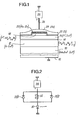
- This drop is of the order of 0.5 V for an Au-Zn contact and for a threshold current of 0.25 A and a series resistance of the order of 2 ⁇ . This drop is significantly lower than the breakdown voltage of the Schottky diode, which is of the order of a few volts.
- the two lateral Ti-Au contacts therefore create very effective electrical isolation.
Landscapes
- Physics & Mathematics (AREA)
- Condensed Matter Physics & Semiconductors (AREA)
- General Physics & Mathematics (AREA)
- Electromagnetism (AREA)
- Optics & Photonics (AREA)
- Geometry (AREA)
- Semiconductor Lasers (AREA)
Applications Claiming Priority (2)
| Application Number | Priority Date | Filing Date | Title |
|---|---|---|---|
| FR8016947 | 1980-07-31 | ||
| FR8016947A FR2488049A1 (fr) | 1980-07-31 | 1980-07-31 | Source lumineuse a jonction semiconductrice, notamment source-laser, utilisant des diodes schottky, et procede de fabrication |
Publications (3)
| Publication Number | Publication Date |
|---|---|
| EP0045678A2 true EP0045678A2 (de) | 1982-02-10 |
| EP0045678A3 EP0045678A3 (en) | 1982-02-24 |
| EP0045678B1 EP0045678B1 (de) | 1985-01-23 |
Family
ID=9244763
Family Applications (1)
| Application Number | Title | Priority Date | Filing Date |
|---|---|---|---|
| EP81401160A Expired EP0045678B1 (de) | 1980-07-31 | 1981-07-21 | Laserquelle mit Halbleiterübergang, die Schottky-Dioden verwendet, und Herstellungsverfahren |
Country Status (6)
| Country | Link |
|---|---|
| US (1) | US4441187A (de) |
| EP (1) | EP0045678B1 (de) |
| JP (1) | JPS5753990A (de) |
| CA (1) | CA1177149A (de) |
| DE (1) | DE3168477D1 (de) |
| FR (1) | FR2488049A1 (de) |
Cited By (4)
| Publication number | Priority date | Publication date | Assignee | Title |
|---|---|---|---|---|
| GB2146489A (en) * | 1983-09-08 | 1985-04-17 | Int Standard Electric Corp | Multimode laser |
| EP0170481A3 (en) * | 1984-07-24 | 1987-05-13 | Nec Corporation | Semiconductor light emitting device |
| EP0544512A1 (de) * | 1991-11-25 | 1993-06-02 | Sharp Kabushiki Kaisha | Lichtemittierende Diode mit baumartiger Oberflächenelektrode |
| EP0589727A3 (en) * | 1992-09-25 | 1994-08-10 | Furukawa Electric Co Ltd | Semiconductor laser device |
Families Citing this family (12)
| Publication number | Priority date | Publication date | Assignee | Title |
|---|---|---|---|---|
| DE3838016A1 (de) * | 1988-11-09 | 1990-05-10 | Siemens Ag | Halbleiterlaser im system gaa1inas |
| JP4189610B2 (ja) | 1998-05-08 | 2008-12-03 | ソニー株式会社 | 光電変換素子およびその製造方法 |
| US6228673B1 (en) * | 1999-05-13 | 2001-05-08 | Hughes Electronics Corporation | Method of fabricating a surface coupled InGaAs photodetector |
| US6791119B2 (en) * | 2001-02-01 | 2004-09-14 | Cree, Inc. | Light emitting diodes including modifications for light extraction |
| US6740906B2 (en) * | 2001-07-23 | 2004-05-25 | Cree, Inc. | Light emitting diodes including modifications for submount bonding |
| US7211833B2 (en) * | 2001-07-23 | 2007-05-01 | Cree, Inc. | Light emitting diodes including barrier layers/sublayers |
| US20030090103A1 (en) * | 2001-11-09 | 2003-05-15 | Thomas Becker | Direct mailing device |
| RU2230411C2 (ru) * | 2002-04-16 | 2004-06-10 | Федеральное государственное унитарное предприятие "Научно-исследовательский институт "Полюс" им.М.Ф.Стельмаха | Инжекционный лазер |
| AU2003263779A1 (en) * | 2002-07-22 | 2004-02-09 | Cree, Inc. | Light emitting diode including barrier layers and manufacturing methods therefor |
| JP2009158550A (ja) * | 2007-12-25 | 2009-07-16 | Sony Corp | 半導体発光素子及びこれを用いた表示装置 |
| DE102008014092A1 (de) * | 2007-12-27 | 2009-07-02 | Osram Opto Semiconductors Gmbh | Kantenemittierender Halbleiterlaserchip mit einem strukturierten Kontaktstreifen |
| DE102016125857B4 (de) | 2016-12-29 | 2022-05-05 | OSRAM Opto Semiconductors Gesellschaft mit beschränkter Haftung | Halbleiterlaserdiode |
Family Cites Families (6)
| Publication number | Priority date | Publication date | Assignee | Title |
|---|---|---|---|---|
| US4149175A (en) * | 1975-06-20 | 1979-04-10 | Matsushita Electric Industrial Co., Ltd. | Solidstate light-emitting device |
| US4048627A (en) * | 1975-11-17 | 1977-09-13 | Rca Corporation | Electroluminescent semiconductor device having a restricted current flow |
| US4206468A (en) * | 1976-05-11 | 1980-06-03 | Thomson-Csf | Contacting structure on a semiconductor arrangement |
| FR2394894A1 (fr) * | 1977-06-17 | 1979-01-12 | Thomson Csf | Dispositif de prise de contact sur un element semiconducteur |
| US4182995A (en) * | 1978-03-16 | 1980-01-08 | Rca Corporation | Laser diode with thermal conducting, current confining film |
| DE2856507A1 (de) * | 1978-12-28 | 1980-07-17 | Amann Markus Christian Dipl In | Halbleiter-laserdiode |
-
1980
- 1980-07-31 FR FR8016947A patent/FR2488049A1/fr active Granted
-
1981
- 1981-07-15 US US06/283,631 patent/US4441187A/en not_active Expired - Lifetime
- 1981-07-21 CA CA000382143A patent/CA1177149A/en not_active Expired
- 1981-07-21 EP EP81401160A patent/EP0045678B1/de not_active Expired
- 1981-07-21 DE DE8181401160T patent/DE3168477D1/de not_active Expired
- 1981-07-30 JP JP56120001A patent/JPS5753990A/ja active Pending
Cited By (6)
| Publication number | Priority date | Publication date | Assignee | Title |
|---|---|---|---|---|
| GB2146489A (en) * | 1983-09-08 | 1985-04-17 | Int Standard Electric Corp | Multimode laser |
| EP0170481A3 (en) * | 1984-07-24 | 1987-05-13 | Nec Corporation | Semiconductor light emitting device |
| EP0544512A1 (de) * | 1991-11-25 | 1993-06-02 | Sharp Kabushiki Kaisha | Lichtemittierende Diode mit baumartiger Oberflächenelektrode |
| US5309001A (en) * | 1991-11-25 | 1994-05-03 | Sharp Kabushiki Kaisha | Light-emitting diode having a surface electrode of a tree-like form |
| EP0778625A3 (de) * | 1991-11-25 | 1997-10-29 | Sharp Kk | Lichtemittierende Diode mit baumartiger Oberflächenelektrode |
| EP0589727A3 (en) * | 1992-09-25 | 1994-08-10 | Furukawa Electric Co Ltd | Semiconductor laser device |
Also Published As
| Publication number | Publication date |
|---|---|
| US4441187A (en) | 1984-04-03 |
| CA1177149A (en) | 1984-10-30 |
| FR2488049A1 (fr) | 1982-02-05 |
| EP0045678B1 (de) | 1985-01-23 |
| EP0045678A3 (en) | 1982-02-24 |
| JPS5753990A (de) | 1982-03-31 |
| FR2488049B1 (de) | 1984-01-06 |
| DE3168477D1 (en) | 1985-03-07 |
Similar Documents
| Publication | Publication Date | Title |
|---|---|---|
| EP0045678B1 (de) | Laserquelle mit Halbleiterübergang, die Schottky-Dioden verwendet, und Herstellungsverfahren | |
| EP0829934B1 (de) | Herstellungsverfahren einer optoelektrischen Halbleitervorrichtung, und Vorrichtung oder Matrix von Vorrichtungen hergestellt unter Verwendung dieses Verfahrens | |
| EP0236189B1 (de) | Monolithische Halbleiterstruktur eines Bipoltransistors mit Heteroübergängen und eines Lasers | |
| EP0782228B1 (de) | Herstellungsverfahren für einen oberflächenemittierenden Laser | |
| FR2695261A1 (fr) | Laser émetteur en surface et son procédé de fabrication. | |
| FR2784795A1 (fr) | Structure comportant une couche mince de materiau composee de zones conductrices et de zones isolantes et procede de fabrication d'une telle structure | |
| EP0566494B1 (de) | Elektronenstrahl gepumpter Laserresonator mit asymmetrischer Halbleiter-Heterostruktur | |
| FR2695761A1 (fr) | Procédé de fabrication de dispositifs électro-optiques à ruban, notamment de lasers, et dispositifs ainsi obtenus. | |
| FR2736211A1 (fr) | Procede de fabrication de dispositifs a semi-conducteur a haute resistance, pour couches d'arret de courant | |
| EP0188147B1 (de) | Verfahren zur Herstellung eines Halbleiterlasers mit vergrabener Streifenstruktur | |
| EP0232662B1 (de) | Monolithische Halbleiterstruktur bestehend aus einem Laser und einem Feldeffekttransistor und deren Herstellungsverfahren | |
| EP0437385B1 (de) | Halbleiterstruktur für optoelektronische Vorrichtung | |
| EP1764887B1 (de) | Optoelektronische Vorrichtung mit einem Laser mit integriertem Modulator und Herstellungsverfahren dafür | |
| EP0817337A1 (de) | Herstellungsverfahren für einen Oberflächenemittierenden Laser | |
| EP0358569B1 (de) | Herstellungsverfahren für einen Halbleiterlaser mit hoher Ausgangsleistung, breiter Bandpasscharakteristik und einer vergrabenen, streifenförmigen BRS-Struktur | |
| FR2716036A1 (fr) | Couche semi-conductrice composée de haute résistance et procédé pour sa croissance cristalline. | |
| FR2604828A1 (fr) | Procede de fabrication d'une diode p+nn+ et d'un transistor bipolaire comportant cette diode, utilisant l'effet de neutralisation des atomes donneurs par l'hydrogene atomique | |
| FR2724068A1 (fr) | Dispositif laser a semi-conducteur et procede de fabrication du dispositif laser a semi-conducteur | |
| EP0218518B1 (de) | Verfahren zur Herstellung eines Halbleiterlasers mit vergrabener Streifenstruktur mit oder ohne Beugungsgitter und nach diesem Verfahren hergestellter Laser | |
| US5917243A (en) | Semiconductor device having ohmic electrode and method of manufacturing the same | |
| EP0096613B1 (de) | Halbleiter-Laservorrichtung mit einem Wellenleiter, der durch einen Gradienten im Brechungsindex gebildet ist und Verfahren zur Herstellung einer solchen Vorrichtung | |
| FR2666455A1 (fr) | Dispositif optoelectronique et application a la realisation d'un laser et d'un photodetecteur. | |
| FR2485823A1 (fr) | Laser semi-conducteur | |
| EP0203848B1 (de) | Verfahren zur Herstellung eines Halbleiterlasers mit Streifengeometrie und ein nach diesem Verfahren hergestellter Laser | |
| EP0610130A1 (de) | Verfahren zur Herstellung einer Halbleiterkomponente, insbesondere eines Lasers mit vergrabener Streifenstruktur und nach diesem Verfahren hergestellte Komponente |
Legal Events
| Date | Code | Title | Description |
|---|---|---|---|
| PUAI | Public reference made under article 153(3) epc to a published international application that has entered the european phase |
Free format text: ORIGINAL CODE: 0009012 |
|
| PUAL | Search report despatched |
Free format text: ORIGINAL CODE: 0009013 |
|
| AK | Designated contracting states |
Designated state(s): DE GB NL |
|
| AK | Designated contracting states |
Designated state(s): DE GB NL |
|
| 17P | Request for examination filed |
Effective date: 19820722 |
|
| GRAA | (expected) grant |
Free format text: ORIGINAL CODE: 0009210 |
|
| AK | Designated contracting states |
Designated state(s): DE GB NL |
|
| REF | Corresponds to: |
Ref document number: 3168477 Country of ref document: DE Date of ref document: 19850307 |
|
| PLBI | Opposition filed |
Free format text: ORIGINAL CODE: 0009260 |
|
| 26 | Opposition filed |
Opponent name: SIEMENS AKTIENGESELLSCHAFT, BERLIN UND MUENCHEN Effective date: 19851022 |
|
| NLR1 | Nl: opposition has been filed with the epo |
Opponent name: SIEMENS AKTIENGESELLSCHAFT |
|
| PGFP | Annual fee paid to national office [announced via postgrant information from national office to epo] |
Ref country code: DE Payment date: 19880611 Year of fee payment: 8 |
|
| PGFP | Annual fee paid to national office [announced via postgrant information from national office to epo] |
Ref country code: NL Payment date: 19880731 Year of fee payment: 8 |
|
| RDAG | Patent revoked |
Free format text: ORIGINAL CODE: 0009271 |
|
| STAA | Information on the status of an ep patent application or granted ep patent |
Free format text: STATUS: PATENT REVOKED |
|
| GBPR | Gb: patent revoked under art. 102 of the ep convention designating the uk as contracting state | ||
| 27W | Patent revoked |
Effective date: 19880623 |
|
| NLR2 | Nl: decision of opposition | ||
| APAH | Appeal reference modified |
Free format text: ORIGINAL CODE: EPIDOSCREFNO |