EP0045895A1 - Disposition pour la modification de la configuration de circuits électriques intégrés - Google Patents
Disposition pour la modification de la configuration de circuits électriques intégrés Download PDFInfo
- Publication number
- EP0045895A1 EP0045895A1 EP81105923A EP81105923A EP0045895A1 EP 0045895 A1 EP0045895 A1 EP 0045895A1 EP 81105923 A EP81105923 A EP 81105923A EP 81105923 A EP81105923 A EP 81105923A EP 0045895 A1 EP0045895 A1 EP 0045895A1
- Authority
- EP
- European Patent Office
- Prior art keywords
- circuit
- amplifier
- arrangement according
- integrated
- electrical
- Prior art date
- Legal status (The legal status is an assumption and is not a legal conclusion. Google has not performed a legal analysis and makes no representation as to the accuracy of the status listed.)
- Withdrawn
Links
Images

Classifications
-
- H—ELECTRICITY
- H10—SEMICONDUCTOR DEVICES; ELECTRIC SOLID-STATE DEVICES NOT OTHERWISE PROVIDED FOR
- H10W—GENERIC PACKAGES, INTERCONNECTIONS, CONNECTORS OR OTHER CONSTRUCTIONAL DETAILS OF DEVICES COVERED BY CLASS H10
- H10W20/00—Interconnections in chips, wafers or substrates
- H10W20/40—Interconnections external to wafers or substrates, e.g. back-end-of-line [BEOL] metallisations or vias connecting to gate electrodes
- H10W20/49—Adaptable interconnections, e.g. fuses or antifuses
- H10W20/493—Fuses, i.e. interconnections changeable from conductive to non-conductive
-
- H—ELECTRICITY
- H01—ELECTRIC ELEMENTS
- H01C—RESISTORS
- H01C17/00—Apparatus or processes specially adapted for manufacturing resistors
- H01C17/22—Apparatus or processes specially adapted for manufacturing resistors adapted for trimming
- H01C17/23—Apparatus or processes specially adapted for manufacturing resistors adapted for trimming by opening or closing resistor geometric tracks of predetermined resistive values, e.g. snapistors
-
- H—ELECTRICITY
- H03—ELECTRONIC CIRCUITRY
- H03F—AMPLIFIERS
- H03F3/00—Amplifiers with only discharge tubes or only semiconductor devices as amplifying elements
- H03F3/45—Differential amplifiers
- H03F3/45071—Differential amplifiers with semiconductor devices only
- H03F3/45479—Differential amplifiers with semiconductor devices only characterised by the way of common mode signal rejection
- H03F3/45484—Differential amplifiers with semiconductor devices only characterised by the way of common mode signal rejection in differential amplifiers with bipolar transistors as the active amplifying circuit
- H03F3/45596—Differential amplifiers with semiconductor devices only characterised by the way of common mode signal rejection in differential amplifiers with bipolar transistors as the active amplifying circuit by offset reduction
- H03F3/45618—Differential amplifiers with semiconductor devices only characterised by the way of common mode signal rejection in differential amplifiers with bipolar transistors as the active amplifying circuit by offset reduction by using balancing means
- H03F3/45623—Differential amplifiers with semiconductor devices only characterised by the way of common mode signal rejection in differential amplifiers with bipolar transistors as the active amplifying circuit by offset reduction by using balancing means using switching means
-
- H—ELECTRICITY
- H03—ELECTRONIC CIRCUITRY
- H03F—AMPLIFIERS
- H03F2203/00—Indexing scheme relating to amplifiers with only discharge tubes or only semiconductor devices as amplifying elements covered by H03F3/00
- H03F2203/45—Indexing scheme relating to differential amplifiers
- H03F2203/45696—Indexing scheme relating to differential amplifiers the LC comprising more than two resistors
-
- H—ELECTRICITY
- H03—ELECTRONIC CIRCUITRY
- H03F—AMPLIFIERS
- H03F2203/00—Indexing scheme relating to amplifiers with only discharge tubes or only semiconductor devices as amplifying elements covered by H03F3/00
- H03F2203/45—Indexing scheme relating to differential amplifiers
- H03F2203/45702—Indexing scheme relating to differential amplifiers the LC comprising two resistors
-
- H—ELECTRICITY
- H03—ELECTRONIC CIRCUITRY
- H03F—AMPLIFIERS
- H03F2203/00—Indexing scheme relating to amplifiers with only discharge tubes or only semiconductor devices as amplifying elements covered by H03F3/00
- H03F2203/45—Indexing scheme relating to differential amplifiers
- H03F2203/45726—Indexing scheme relating to differential amplifiers the LC comprising more than one switch, which are not cross coupled
Definitions
- the present invention relates to an arrangement for changing the electrical circuit configuration of integrated semiconductor circuits for the setting and the adjustment of circuit parameters, such as references, switching thresholds, zero errors (offset voltages) or function reversal.
- Circuit system is understood to mean the semiconductor body containing the electrical functional units of a circuit with conductor tracks running thereon for the electrical connection of the individual functional units to one another, as well as connecting electrodes for the contacting of external leads.
- the circuit system is thus the finished integrated semiconductor circuit without external leads and without a housing.
- piezoresistive influences occur in the components of all semiconductor circuits, in particular integrated in silicon, due to unavoidable mechanical stresses.
- the mechanical stresses occur, for example, when the circuit systems are installed in a housing.
- Piezo effects of this type also have a particularly strong effect in the case of integrated semiconductor circuits in which Hall generators are integrated as sensors, since such Integrated semiconductor circuits are relatively large and the Hall generators emit relatively small useful signals, so that successor amplifiers are required in any case.
- the piezo effects therefore lead to very unpleasant scattering of the magnetic levels in integrated semiconductor circuits in which Hall generators are integrated. The problem is all the more serious since a perfect pre-measurement on the system is not possible because subsequent assembly steps can change the mechanical stresses.
- Such semiconductor circuits are further processed in other housings in order to create a larger assembly unit, mechanical stresses can occur again.
- An example of such further processing of an integrated circuit in another housing is e.g. the production of a magnetic barrier with a magnetic field-controlled integrated semiconductor circuit which contains a Hall generator as a magnetic sensor.
- the present invention is therefore based on the object of providing a simple possibility for setting and comparing circuit parameters in integrated circuits.
- circuit connections which are provided selectively in the circuit configuration of the integrated semiconductor circuits and are accessible outside the circuit chips and can be mechanically separated without mechanical or electrical loading or change in the circuit chips.
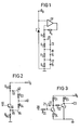
- an input of an operational amplifier OP is connected to a Zener diode Z, to which a reference potential is set via an operating voltage + U B.
- Another input of the operational amplifier OP lies across a negative feedback resistor R K at the output of the operational amplifier OP.
- the negative feedback input of the operational amplifier OP is connected to ground via a voltage divider formed from resistors R 1 to R 4 .
- the resistors R 2 , R 3 and R 4 are bridged by short-circuit bridging 10, 11 and 12, respectively.
- these short-circuit bridges 10 to 12 are accessible outside the circuit chip containing this amplifier and can be mechanically separated. These separations are schematically indicated by an "X" 13, 14 and 15, respectively.
- X 13
- the short-circuit bypasses 10-12 there are different divider ratios in the voltage divider R 1 -R 4 , as a result of which different negative feedback values can be set.
- FIG. 2 shows a transistor amplifier stage with a transistor T 60 ' which can be controlled by an input 60, a resistor R 61 connected to the operating voltage + U B in its collector circuit and a resistor R 61 in its emitter branch
- Resistance R 62 lies.
- the series connection of two resistors R 63 and R 64 ' lies between the collector and emitter of transistor T 60 via line connections 62 and 64.
- the connection point of the two resistors R 63 and R 64 forms an output 61 of the transistor amplifier stage.
- This transistor amplification stage normally works as a push-pull stage. By opening one of the two line connections 62 or 64, this transistor amplifier stage can be converted into a single-ended stage in an emitter circuit (separation at a point 65) or as an emitter follower (separation at a point (63)).
- FIG. 3 shows an embodiment of a two-stage amplifier, in which an amplifier stage is formed by a transistor T 1 with a load resistor R 21 and a transistor T 2 with a load resistor R 23 .
- the operating points of the amplifier stages are set from a voltage U B via the resistors R 21 and R 23 .
- An input signal is coupled into the amplifier from an input 20 via a resistor R2 0.
- a negative feedback resistor R 24 is located in the emitter circuit.
- the first amplifier stage is coupled from the collector of transistor T 1 via a resistor R 22 to the base of transistor T 2 of the second amplifier stage.
- An output signal of the amplifier can be taken off at an output 23.
- a short-circuit bypass 21 is provided between the collector and the base of the transistor T 1 , which is accessible and mechanically separable when the amplifier is integrated outside the circuit chip containing the amplifier. This separation possibility is indicated schematically by an "X" 22.
- phase difference 180 ° at the output of the first amplifier stage, ie at the collector of the transistor T 1 .
- This phase difference is transmitted to the output 23 via the second amplifier stage with the transistor T 2 , so that a phase reversal at the output 23 can thus be achieved by mechanically separating the short-circuit connection 21.
- FIG. 4 shows a circuit arrangement with a Hall generator 36, in the control circuit of which a control current is fed from a current source I H.
- a magnetic field to be detected can pass through the Hall generator 36 in a manner not shown, for example perpendicular to the plane of the drawing. Since the function of Hall generators is basically known, the circuitry is only shown in principle. It is therefore unnecessary to go into detail about how it works.
- the Hall path of the Hall generator 36 is coupled to inputs 37 and 38 of a differential amplifier 31 , which contains two transistors T 30 and T 31 directly coupled to their emitters, the emitters of these two transistors being connected to a current source I O.
- a trimming resistor network 30 which is formed by resistors R A1 and R A2 and bypasses 32 and 33 for these resistors.
- the trimming resistor network 30 is still connected to an operating voltage + U B for the differential amplifier 31.
- the circuit arrangement described above can now be integrated overall in a semiconductor circuit, in which case the above-mentioned piezo effects can occur due to mechanical stresses in the semiconductor circuit.
- the bridges 32 and 33 for the resistors R A1 and R A2 in the trimming resistor network 30 can be selectively separated. This is indicated schematically by crosses 34 and 35 in the bridges 32 and 33. This makes it possible to switch on either only the resistor R A1 , the resistor R A2 or both resistors in the circuit of the differential amplifier 31 in order to be able to selectively compensate for electrical interference signals or level shifts caused by mechanical tension.
- the trimming resistor network can also be constructed in a more complex manner. Such a possibility is shown in FIG. 5.
- the trimming resistor network 30 contains two resistors R A11 and R A12 or R A21 and R A22 each in a branch, each with a bypass 41-1, 41-2 or 42-1, 42-2 for each a resistor, in which case four separation options 43-1, 43-2 and 44-1, 44-2 are available.
- resistance intervals can also be selected similarly to the steps of an analog-digital converter, for example 1 R, 2 R, 4 R, etc., so that 8 stages and 16 stages can be implemented with 16 stages.
- FIG. 6 schematically shows an embodiment of an integrated semiconductor circuit mounted in a so-called micropack.
- micropack For the principle of assembling systems of integrated semiconductor circuits in micropack construction, reference is made to Siemens Components Report 16 (1978) Issue 2, pages 40 to 44.
- a semiconductor system 51 having connection electrodes 52 is applied to a micropack film 50, on which a conductor track pattern 53 with connection pads 54 is prefabricated for the integrated circuit.
- the conductor tracks 53 contact the connection electrodes 52 of the semiconductor system 51.
- the semiconductor system 51 contains a trimming resistor network (not shown) in the sense of the embodiments according to the figures explained above, which is electrically accessible via the conductor tracks 53.
- a comparison to compensate for mechanical tensions after the semiconductor system 51 has been installed in the micropack can be carried out by cutting certain conductor tracks 53 in the micropack. Such severing possibilities are represented in FIG. 6 by crosses 55-1 to 55-4, for example.
- the conductor tracks can be cut, for example, by stamping.
- a micropack of the type described above is further processed, for example installed in a plastic housing of a conventional type, then a further improvement in the compensation of mechanical stresses can be achieved, for example, also due to temperature loads, in that the semiconductor system 51 with a non-magnetic metal cap 56 is covered, for example, from aluminum or brass.
- a cap has the further advantage that it ensures an additional shielding effect against electrical fields, for example when using the circuits in the electronics of motor vehicles.
Landscapes
- Engineering & Computer Science (AREA)
- Manufacturing & Machinery (AREA)
- Microelectronics & Electronic Packaging (AREA)
- Power Engineering (AREA)
- Semiconductor Integrated Circuits (AREA)
- Hall/Mr Elements (AREA)
- Logic Circuits (AREA)
- Amplifiers (AREA)
- Design And Manufacture Of Integrated Circuits (AREA)
Applications Claiming Priority (2)
| Application Number | Priority Date | Filing Date | Title |
|---|---|---|---|
| DE19803030620 DE3030620A1 (de) | 1980-08-13 | 1980-08-13 | Anordnung zur aenderung der elektrischen schaltungskonfiguration von integrierten halbleiterschaltkreisen |
| DE3030620 | 1980-08-13 |
Publications (1)
| Publication Number | Publication Date |
|---|---|
| EP0045895A1 true EP0045895A1 (fr) | 1982-02-17 |
Family
ID=6109541
Family Applications (1)
| Application Number | Title | Priority Date | Filing Date |
|---|---|---|---|
| EP81105923A Withdrawn EP0045895A1 (fr) | 1980-08-13 | 1981-07-27 | Disposition pour la modification de la configuration de circuits électriques intégrés |
Country Status (4)
| Country | Link |
|---|---|
| US (1) | US4438347A (fr) |
| EP (1) | EP0045895A1 (fr) |
| JP (1) | JPS5759372A (fr) |
| DE (1) | DE3030620A1 (fr) |
Cited By (5)
| Publication number | Priority date | Publication date | Assignee | Title |
|---|---|---|---|---|
| GB2230625A (en) * | 1989-01-18 | 1990-10-24 | Seiko Instr Inc | Voltage regulator |
| EP0335634A3 (fr) * | 1988-03-28 | 1990-11-28 | Seiko Instruments Inc. | Circuit intégré comprenant un circuit de détection de voltage |
| EP0685887A1 (fr) * | 1994-05-30 | 1995-12-06 | STMicroelectronics S.r.l. | Circuit pour la sélection d'options de conception dans un circuit intégré |
| US6100747A (en) * | 1994-05-30 | 2000-08-08 | Stmicroelectronics, S.R.L. | Device for selecting design options in an integrated circuit |
| US6215170B1 (en) | 1996-12-31 | 2001-04-10 | Stmicroelectronics, Inc. | Structure for single conductor acting as ground and capacitor plate electrode using reduced area |
Families Citing this family (64)
| Publication number | Priority date | Publication date | Assignee | Title |
|---|---|---|---|---|
| US4792920A (en) * | 1983-06-29 | 1988-12-20 | Canon Denshi Kabushiki Kaisha | Interface providing impedance matching by selective connection of a resistor array to a power supply |
| JPS60254763A (ja) * | 1984-05-31 | 1985-12-16 | Sanken Electric Co Ltd | 集積回路の製造方法 |
| JPH0233644A (ja) * | 1988-07-15 | 1990-02-02 | Ncr Corp | フレキシブル基板を用いた固有コードの設定方法及び装置 |
| US5079442A (en) * | 1990-03-28 | 1992-01-07 | Advanced Micro Devices, Inc. | Apparatus adaptable for use as a replacement output driver in a signal generating circuit |
| DE10036283A1 (de) * | 2000-07-26 | 2002-02-07 | Bosch Gmbh Robert | Laserdiodenanordnung |
| TW573335B (en) * | 2001-08-28 | 2004-01-21 | Anachip Corp | Adjustment system, method and apparatus of using magnetic field to conduct micro-adjustment onto packaged chip |
| US9823090B2 (en) | 2014-10-31 | 2017-11-21 | Allegro Microsystems, Llc | Magnetic field sensor for sensing a movement of a target object |
| US7923996B2 (en) | 2008-02-26 | 2011-04-12 | Allegro Microsystems, Inc. | Magnetic field sensor with automatic sensitivity adjustment |
| DE112010000848B4 (de) | 2009-02-17 | 2018-04-05 | Allegro Microsystems, Llc | Schaltungen und Verfahren zum Erzeugen eines Selbsttests eines Magnetfeldsensors |
| WO2011011479A1 (fr) | 2009-07-22 | 2011-01-27 | Allegro Microsystems, Inc. | Circuits et procédés pour mettre en place un mode de fonctionnement de diagnostic dans un capteur de champ magnétique |
| JP2012168899A (ja) * | 2011-02-16 | 2012-09-06 | Seiko Instruments Inc | ボルテージレギュレータ |
| US8680846B2 (en) | 2011-04-27 | 2014-03-25 | Allegro Microsystems, Llc | Circuits and methods for self-calibrating or self-testing a magnetic field sensor |
| US8604777B2 (en) | 2011-07-13 | 2013-12-10 | Allegro Microsystems, Llc | Current sensor with calibration for a current divider configuration |
| US9201122B2 (en) | 2012-02-16 | 2015-12-01 | Allegro Microsystems, Llc | Circuits and methods using adjustable feedback for self-calibrating or self-testing a magnetic field sensor with an adjustable time constant |
| US9817078B2 (en) | 2012-05-10 | 2017-11-14 | Allegro Microsystems Llc | Methods and apparatus for magnetic sensor having integrated coil |
| US9383425B2 (en) | 2012-12-28 | 2016-07-05 | Allegro Microsystems, Llc | Methods and apparatus for a current sensor having fault detection and self test functionality |
| US10725100B2 (en) | 2013-03-15 | 2020-07-28 | Allegro Microsystems, Llc | Methods and apparatus for magnetic sensor having an externally accessible coil |
| US10495699B2 (en) | 2013-07-19 | 2019-12-03 | Allegro Microsystems, Llc | Methods and apparatus for magnetic sensor having an integrated coil or magnet to detect a non-ferromagnetic target |
| US10145908B2 (en) | 2013-07-19 | 2018-12-04 | Allegro Microsystems, Llc | Method and apparatus for magnetic sensor producing a changing magnetic field |
| US9810519B2 (en) | 2013-07-19 | 2017-11-07 | Allegro Microsystems, Llc | Arrangements for magnetic field sensors that act as tooth detectors |
| EP3080627B1 (fr) | 2013-12-26 | 2020-10-14 | Allegro MicroSystems, LLC | Procédés et appareil pour diagnostics de capteurs |
| US9645220B2 (en) | 2014-04-17 | 2017-05-09 | Allegro Microsystems, Llc | Circuits and methods for self-calibrating or self-testing a magnetic field sensor using phase discrimination |
| US9735773B2 (en) | 2014-04-29 | 2017-08-15 | Allegro Microsystems, Llc | Systems and methods for sensing current through a low-side field effect transistor |
| US9739846B2 (en) | 2014-10-03 | 2017-08-22 | Allegro Microsystems, Llc | Magnetic field sensors with self test |
| US9719806B2 (en) | 2014-10-31 | 2017-08-01 | Allegro Microsystems, Llc | Magnetic field sensor for sensing a movement of a ferromagnetic target object |
| US10712403B2 (en) | 2014-10-31 | 2020-07-14 | Allegro Microsystems, Llc | Magnetic field sensor and electronic circuit that pass amplifier current through a magnetoresistance element |
| US9823092B2 (en) | 2014-10-31 | 2017-11-21 | Allegro Microsystems, Llc | Magnetic field sensor providing a movement detector |
| US9720054B2 (en) | 2014-10-31 | 2017-08-01 | Allegro Microsystems, Llc | Magnetic field sensor and electronic circuit that pass amplifier current through a magnetoresistance element |
| US10466298B2 (en) | 2014-11-14 | 2019-11-05 | Allegro Microsystems, Llc | Magnetic field sensor with shared path amplifier and analog-to-digital-converter |
| US9804249B2 (en) | 2014-11-14 | 2017-10-31 | Allegro Microsystems, Llc | Dual-path analog to digital converter |
| US9841485B2 (en) | 2014-11-14 | 2017-12-12 | Allegro Microsystems, Llc | Magnetic field sensor having calibration circuitry and techniques |
| US9638764B2 (en) | 2015-04-08 | 2017-05-02 | Allegro Microsystems, Llc | Electronic circuit for driving a hall effect element with a current compensated for substrate stress |
| US9851417B2 (en) | 2015-07-28 | 2017-12-26 | Allegro Microsystems, Llc | Structure and system for simultaneous sensing a magnetic field and mechanical stress |
| US10107873B2 (en) | 2016-03-10 | 2018-10-23 | Allegro Microsystems, Llc | Electronic circuit for compensating a sensitivity drift of a hall effect element due to stress |
| US10132879B2 (en) | 2016-05-23 | 2018-11-20 | Allegro Microsystems, Llc | Gain equalization for multiple axis magnetic field sensing |
| US10260905B2 (en) | 2016-06-08 | 2019-04-16 | Allegro Microsystems, Llc | Arrangements for magnetic field sensors to cancel offset variations |
| US10012518B2 (en) | 2016-06-08 | 2018-07-03 | Allegro Microsystems, Llc | Magnetic field sensor for sensing a proximity of an object |
| US10041810B2 (en) | 2016-06-08 | 2018-08-07 | Allegro Microsystems, Llc | Arrangements for magnetic field sensors that act as movement detectors |
| US10162017B2 (en) | 2016-07-12 | 2018-12-25 | Allegro Microsystems, Llc | Systems and methods for reducing high order hall plate sensitivity temperature coefficients |
| US11428755B2 (en) | 2017-05-26 | 2022-08-30 | Allegro Microsystems, Llc | Coil actuated sensor with sensitivity detection |
| US10837943B2 (en) | 2017-05-26 | 2020-11-17 | Allegro Microsystems, Llc | Magnetic field sensor with error calculation |
| US10996289B2 (en) | 2017-05-26 | 2021-05-04 | Allegro Microsystems, Llc | Coil actuated position sensor with reflected magnetic field |
| US10310028B2 (en) | 2017-05-26 | 2019-06-04 | Allegro Microsystems, Llc | Coil actuated pressure sensor |
| US10324141B2 (en) | 2017-05-26 | 2019-06-18 | Allegro Microsystems, Llc | Packages for coil actuated position sensors |
| US10641842B2 (en) | 2017-05-26 | 2020-05-05 | Allegro Microsystems, Llc | Targets for coil actuated position sensors |
| US10520559B2 (en) | 2017-08-14 | 2019-12-31 | Allegro Microsystems, Llc | Arrangements for Hall effect elements and vertical epi resistors upon a substrate |
| US10866117B2 (en) | 2018-03-01 | 2020-12-15 | Allegro Microsystems, Llc | Magnetic field influence during rotation movement of magnetic target |
| US11255700B2 (en) | 2018-08-06 | 2022-02-22 | Allegro Microsystems, Llc | Magnetic field sensor |
| US10823586B2 (en) | 2018-12-26 | 2020-11-03 | Allegro Microsystems, Llc | Magnetic field sensor having unequally spaced magnetic field sensing elements |
| US11061084B2 (en) | 2019-03-07 | 2021-07-13 | Allegro Microsystems, Llc | Coil actuated pressure sensor and deflectable substrate |
| JP7297479B2 (ja) * | 2019-03-15 | 2023-06-26 | エイブリック株式会社 | 半導体装置 |
| US10955306B2 (en) | 2019-04-22 | 2021-03-23 | Allegro Microsystems, Llc | Coil actuated pressure sensor and deformable substrate |
| US11237020B2 (en) | 2019-11-14 | 2022-02-01 | Allegro Microsystems, Llc | Magnetic field sensor having two rows of magnetic field sensing elements for measuring an angle of rotation of a magnet |
| US11280637B2 (en) | 2019-11-14 | 2022-03-22 | Allegro Microsystems, Llc | High performance magnetic angle sensor |
| US11194004B2 (en) | 2020-02-12 | 2021-12-07 | Allegro Microsystems, Llc | Diagnostic circuits and methods for sensor test circuits |
| US11169223B2 (en) | 2020-03-23 | 2021-11-09 | Allegro Microsystems, Llc | Hall element signal calibrating in angle sensor |
| US11262422B2 (en) | 2020-05-08 | 2022-03-01 | Allegro Microsystems, Llc | Stray-field-immune coil-activated position sensor |
| US11493361B2 (en) | 2021-02-26 | 2022-11-08 | Allegro Microsystems, Llc | Stray field immune coil-activated sensor |
| US11630130B2 (en) | 2021-03-31 | 2023-04-18 | Allegro Microsystems, Llc | Channel sensitivity matching |
| US11578997B1 (en) | 2021-08-24 | 2023-02-14 | Allegro Microsystems, Llc | Angle sensor using eddy currents |
| US11994541B2 (en) | 2022-04-15 | 2024-05-28 | Allegro Microsystems, Llc | Current sensor assemblies for low currents |
| US12510611B2 (en) | 2023-11-07 | 2025-12-30 | Allegro Microsystems, Llc | TMR sensor having magnetic field generation for pillar stimulation |
| US12455301B2 (en) | 2023-12-11 | 2025-10-28 | Allegro Microsystems, Llc | Hall plate current sensor having stress compensation |
| US12523717B2 (en) | 2024-02-15 | 2026-01-13 | Allegro Microsystems, Llc | Closed loop magnetic field sensor with current control |
Citations (4)
| Publication number | Priority date | Publication date | Assignee | Title |
|---|---|---|---|---|
| DE1791024B1 (de) * | 1967-09-01 | 1971-05-19 | Lucas Industries Ltd | Leiterplatte und verfahren zu deren herstellung |
| GB1500394A (en) * | 1976-04-27 | 1978-02-08 | Welwyn Electric Ltd | Electrical resistor network |
| US4182024A (en) * | 1977-12-15 | 1980-01-08 | National Semiconductor Corporation | Automatic control of integrated circuit trimming |
| US4201970A (en) * | 1978-08-07 | 1980-05-06 | Rca Corporation | Method and apparatus for trimming resistors |
Family Cites Families (5)
| Publication number | Priority date | Publication date | Assignee | Title |
|---|---|---|---|---|
| US3758745A (en) | 1971-09-07 | 1973-09-11 | Microsystems Int Ltd | Substrate positioned determination structure and method |
| US3820152A (en) | 1973-04-24 | 1974-06-25 | Du Pont | Circuit package with fugitive shorting bar |
| DE2614781B2 (de) | 1976-04-06 | 1979-04-05 | Robert Bosch Gmbh, 7000 Stuttgart | Integrierte Schaltungsanordnung |
| US4100437A (en) | 1976-07-29 | 1978-07-11 | Intel Corporation | MOS reference voltage circuit |
| US4225878A (en) | 1979-03-08 | 1980-09-30 | National Semiconductor Corporation | Integrated circuit on chip trimming |
-
1980
- 1980-08-13 DE DE19803030620 patent/DE3030620A1/de not_active Withdrawn
-
1981
- 1981-07-27 EP EP81105923A patent/EP0045895A1/fr not_active Withdrawn
- 1981-08-07 US US06/291,112 patent/US4438347A/en not_active Expired - Fee Related
- 1981-08-13 JP JP56127321A patent/JPS5759372A/ja active Pending
Patent Citations (4)
| Publication number | Priority date | Publication date | Assignee | Title |
|---|---|---|---|---|
| DE1791024B1 (de) * | 1967-09-01 | 1971-05-19 | Lucas Industries Ltd | Leiterplatte und verfahren zu deren herstellung |
| GB1500394A (en) * | 1976-04-27 | 1978-02-08 | Welwyn Electric Ltd | Electrical resistor network |
| US4182024A (en) * | 1977-12-15 | 1980-01-08 | National Semiconductor Corporation | Automatic control of integrated circuit trimming |
| US4201970A (en) * | 1978-08-07 | 1980-05-06 | Rca Corporation | Method and apparatus for trimming resistors |
Non-Patent Citations (1)
| Title |
|---|
| IEEE Journal of Solid-State Circuits, Band SC-11, Nr. 6, Dezember 1976 New York J.J. PRICE "A Passive Laser-Trimming Technique to Improve the Linearity of a 10-Bit D/A Converter", seiten 789 bis 794 *seite 793, linke spalte, letzter Absatz bis seite 794, linke spalte, erster Absatz; fig. 5, 6, 7, tabelle 1* * |
Cited By (6)
| Publication number | Priority date | Publication date | Assignee | Title |
|---|---|---|---|---|
| EP0335634A3 (fr) * | 1988-03-28 | 1990-11-28 | Seiko Instruments Inc. | Circuit intégré comprenant un circuit de détection de voltage |
| GB2230625A (en) * | 1989-01-18 | 1990-10-24 | Seiko Instr Inc | Voltage regulator |
| GB2230625B (en) * | 1989-01-18 | 1993-05-12 | Seiko Instr Inc | A voltage regulator |
| EP0685887A1 (fr) * | 1994-05-30 | 1995-12-06 | STMicroelectronics S.r.l. | Circuit pour la sélection d'options de conception dans un circuit intégré |
| US6100747A (en) * | 1994-05-30 | 2000-08-08 | Stmicroelectronics, S.R.L. | Device for selecting design options in an integrated circuit |
| US6215170B1 (en) | 1996-12-31 | 2001-04-10 | Stmicroelectronics, Inc. | Structure for single conductor acting as ground and capacitor plate electrode using reduced area |
Also Published As
| Publication number | Publication date |
|---|---|
| JPS5759372A (en) | 1982-04-09 |
| DE3030620A1 (de) | 1982-03-11 |
| US4438347A (en) | 1984-03-20 |
Similar Documents
| Publication | Publication Date | Title |
|---|---|---|
| EP0045895A1 (fr) | Disposition pour la modification de la configuration de circuits électriques intégrés | |
| EP0363512B1 (fr) | Dispositif sans-contact pour établir la vitesse d'une roue dentée | |
| DE2825882C2 (de) | Schaltungsanordnung zur Reduzierung niederfrequenter Störspannung und Offsetspannung bei einer Verstärkerschaltung | |
| EP0218011B1 (fr) | Circuit détecteur d'intrusion sensible aux radiations infrarouges | |
| DE3100297C2 (fr) | ||
| EP0236525A1 (fr) | Ligne à retard intégrée pour signaux numériques utilisant des transistors à effet de champ | |
| DE19544863A1 (de) | Sensorvorrichtung | |
| DE3424052A1 (de) | Signalumformer | |
| EP0725996B1 (fr) | Circuit de commande | |
| DE2305291C3 (de) | Regelschaltung zur Regelung der Amplitude eines Signals | |
| DE102021101653A1 (de) | Spannungsversorgung | |
| DE10145655A1 (de) | Schaltungsanordnung für einen gradiometrischen Stromsensor sowie ein die Schaltungsanordnung aufweisender Sensorchip | |
| DE69528845T2 (de) | N-bit umsetzer mit n-1-grössenverstärkern und n-vergleichern | |
| DE2839459C2 (de) | Schaltungsanordnung zur Signalpegelumsetzung | |
| DE2924171C2 (fr) | ||
| DE2722581C3 (de) | Schaltungsanordnung zur Signalaufbereitung von Ausgangssignalen eines Feldplattengebers bei Raddrehzahlgebern von Fahrzeugen | |
| DE3832378C1 (fr) | ||
| DE3228785C2 (fr) | ||
| WO2006125407A1 (fr) | Dispositif pour mesurer l'intensite d'un courant | |
| EP0051578A2 (fr) | Etage de sortie pour des lignes de signaux à audio-fréquences | |
| DE102004010785B4 (de) | Konfigurierbarer Eingangsverstärker für Positionsmesseinrichtungen | |
| DE4336726A1 (de) | Schaltung zur Strommessung | |
| EP0727644A1 (fr) | Dispositif détecteur | |
| DE3432561A1 (de) | Transistor-praezisionsstromquelle mit differenzeingang | |
| WO1993011607A1 (fr) | Procede et circuit pour la mesure de courants de particules |
Legal Events
| Date | Code | Title | Description |
|---|---|---|---|
| PUAI | Public reference made under article 153(3) epc to a published international application that has entered the european phase |
Free format text: ORIGINAL CODE: 0009012 |
|
| 17P | Request for examination filed |
Effective date: 19811028 |
|
| AK | Designated contracting states |
Designated state(s): DE FR GB IT |
|
| STAA | Information on the status of an ep patent application or granted ep patent |
Free format text: STATUS: THE APPLICATION IS DEEMED TO BE WITHDRAWN |
|
| 18D | Application deemed to be withdrawn |
Effective date: 19850531 |
|
| RIN1 | Information on inventor provided before grant (corrected) |
Inventor name: GEHRING, GERHARD, DIPL.-ING. |