EP0046708A2 - Digitale Signalverarbeitungsschaltung in verteilter Arithmetik mit Verwendung eines Multiplexers am Eingang eines Speichers - Google Patents
Digitale Signalverarbeitungsschaltung in verteilter Arithmetik mit Verwendung eines Multiplexers am Eingang eines Speichers Download PDFInfo
- Publication number
- EP0046708A2 EP0046708A2 EP81401311A EP81401311A EP0046708A2 EP 0046708 A2 EP0046708 A2 EP 0046708A2 EP 81401311 A EP81401311 A EP 81401311A EP 81401311 A EP81401311 A EP 81401311A EP 0046708 A2 EP0046708 A2 EP 0046708A2
- Authority
- EP
- European Patent Office
- Prior art keywords
- memory
- counter
- outputs
- registers
- blocks
- Prior art date
- Legal status (The legal status is an assumption and is not a legal conclusion. Google has not performed a legal analysis and makes no representation as to the accuracy of the status listed.)
- Granted
Links
- 230000015654 memory Effects 0.000 title claims abstract description 82
- 238000012545 processing Methods 0.000 title claims abstract description 11
- 238000001914 filtration Methods 0.000 claims description 2
- 238000007792 addition Methods 0.000 description 5
- 238000000034 method Methods 0.000 description 5
- 238000004364 calculation method Methods 0.000 description 3
- 235000021183 entrée Nutrition 0.000 description 3
- 101000822695 Clostridium perfringens (strain 13 / Type A) Small, acid-soluble spore protein C1 Proteins 0.000 description 2
- 101000655262 Clostridium perfringens (strain 13 / Type A) Small, acid-soluble spore protein C2 Proteins 0.000 description 2
- 101000655256 Paraclostridium bifermentans Small, acid-soluble spore protein alpha Proteins 0.000 description 2
- 101000655264 Paraclostridium bifermentans Small, acid-soluble spore protein beta Proteins 0.000 description 2
- 241000287107 Passer Species 0.000 description 2
- 230000008520 organization Effects 0.000 description 2
- 230000009467 reduction Effects 0.000 description 2
- 238000012552 review Methods 0.000 description 2
- 241001529297 Coregonus peled Species 0.000 description 1
- 241001486931 Sillago burrus Species 0.000 description 1
- 238000013459 approach Methods 0.000 description 1
- 230000005540 biological transmission Effects 0.000 description 1
- 230000000295 complement effect Effects 0.000 description 1
- 230000003111 delayed effect Effects 0.000 description 1
- 230000000694 effects Effects 0.000 description 1
- 230000006870 function Effects 0.000 description 1
- 238000004519 manufacturing process Methods 0.000 description 1
- 238000012986 modification Methods 0.000 description 1
- 230000004048 modification Effects 0.000 description 1
- 230000008569 process Effects 0.000 description 1
- 230000000717 retained effect Effects 0.000 description 1
- 238000005070 sampling Methods 0.000 description 1
- 238000012546 transfer Methods 0.000 description 1
Images


Classifications
-
- H—ELECTRICITY
- H03—ELECTRONIC CIRCUITRY
- H03H—IMPEDANCE NETWORKS, e.g. RESONANT CIRCUITS; RESONATORS
- H03H17/00—Networks using digital techniques
- H03H17/02—Frequency selective networks
- H03H17/0223—Computation saving measures; Accelerating measures
- H03H17/0238—Measures concerning the arithmetic used
- H03H17/0241—Distributed arithmetic
Definitions
- the present invention relates to a digital processing circuit in distributed arithmetic. It finds an application in the production of digital filters usable in particular in telecommunications.
- the digital processing carried out by the circuit of the invention is a weighted sum which can be expressed by the relation: where u k denotes different digital signals of rank k and where a k denotes weighting coefficients.
- recursive digital filtering which is classically characterized by an expression of the form: where x nk denotes input signals of rank nk, y nk output signals of rank nk reinjected at the input of the filter, a k coefficients of the non-recursive part, whose order is p and b k of coefficients of the recursive part, whose order is q; the index n takes all the values, is an integer and characterizes the rank of the output signal.
- a recursive digital filter able to carry out such a processing comprises p + l inputs receiving the signals xk and q inputs receiving the signals y k , ie in total p + q + 1 inputs; it also includes an output delivering the sequence of signals y n .
- the invention is part of a particular digital processing technique called "distributed arithmetic". This technique is described in US Patent No. 3,777,130 issued December 4, 1973 to A. CROISIER, DJ ESTEBAN, ME LEVILION and V. RISO and entitled “Digital Filter for PCM Encoded Signals” as well as in the article by A PELED and B. LIU entitled “A new Hardware Realization of Digital Filters” published in the review “IEEE Trans. On ASSP" vol. ASSP 22, pp 456-462 in December 1974. In addition, the article by C.S. BURRUS entitled “Digital Filter Structures Described by Distributed Arithmetic” published in the review “IEEE Trans on Circuits and Systems", vol.
- u k (j) which appears in the expression in parentheses is the bit of rank j of u k and this bit can only take two values: 0 or 1.
- a 1 there are therefore only two possible values: 0 or a 1 .
- a 2 which can only take the two values 0 and a 2 ; there are therefore only 4 possible values for the sum of these two products, namely 0, a 1 , a 2 , or a l + a 2 .
- That of these 2 P values which must be retained to form w j is defined by the set of p bits of rank j of the input signals, namely u l (j), u 2 (j) ... u p (j).
- the quantities w. are written in a memory of 2 P words of m bits, if m is the number of bits necessary to express these partial sums.
- the word corresponding to a particular w is located, in this memory, at the address corresponding to the p bits of rank j of the input signals u k .
- the number m is determined from the constraints of the problem to be treated and it can be reduced in two different ways: by truncating the coefficients a k as in a conventional embodiment ,. or by direct truncation of the quantities w j (but then the treatment is no longer strictly linear).
- the latter method is described in the article by R. LAGADEC and D. PELLONI entitled "A Model for Distributed Arithmetic for Filters with Post-Quantized Look-up Table" published in "National Telecommunication Conference" 1977, pp 29: 3 -1 to 29: 3-6.
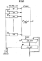
- FIG. 1 The hardware organization of such a circuit is illustrated in FIG. 1.
- the circuit represented comprises: p registers - series 10/1, 10/2, ..., 10 / p of r bits receiving the p input signals 20, a read only memory of 2 P words of m bits, an adder-subtractor 30, a register with parallel inputs and parallel outputs 40 that can be shifted and a clock circuit 50.
- the memory has p inputs connected to the outputs of the p input registers and it contains the following 2 p quantities: where ⁇ k takes the values 0 or 1; the address of each quantity is constituted by p bits applied to the p inputs.
- the circuit also includes a memory 20 with p + q + 1 inputs connected to the output of the registers, this memory containing 2 p + q + 1 words of m bits, these words being the quantities: where the ⁇ j are equal to 0 or 1, j going from 1 to p + q + l.
- the circuit finally comprises the arithmetic processing members already mentioned, namely: an adder-subtractor 30, a register-accumulator 40 with parallel inputs and parallel outputs, as well as a clock 50 ensuring the proper course of operations (shifting of registers, loading of parallel registers, resetting of the accumulator at the end of the cycle).
- the frequency of reading the memory and shifting the registers is equal to rf E if f E is the sampling frequency of the digital filter. If the data x k enter the device in serial form, low weight at the head, at the right rate and with the right number r of bits, the first register 10/0 is not essential. If it is maintained, with a sort of buffer register role, the result is delayed by a period l / f E. In some applications, the data is presented in parallel form: the first register must then be loaded in parallel.
- the size of the memory becomes large as soon as the orders p and q of the filter reach values of the order of 6, which corresponds to the templates necessary for the transmission of information by coded pulses (MIC).
- M multiplexers can be arranged at the memory output, as described in the article by CS BURRUS cited above. These multiplexers have M inputs and one output. Such a multiplexer will be symbolized subsequently by the notation M 1. It is controlled by a modulo M counter with outputs which receives clock pulses.
- the memory is then composed of M different memories, each of 2 n words of m bits, these memories having n addressing inputs and an output.
- the circuit includes a total of nM input registers divided into n groups each associated with a memory.
- the size of the storage unit is then M.2 n words of m bits, which is less than the size of 2 nM that a single memory without multiplexers should have in order to be able to process nM input signals.
- the invention retains a slightly different arrangement which consists in placing the multiplexers at the input of the memory and no longer at the output. This makes it possible to use a single memory (instead of M) and n multiplexers M ⁇ 1 instead of m.
- the corresponding circuit is shown in Figure 3. It also includes nM input registers divided into n groups respectively 10/1, 10/2, ...
- 10 / M for the first group 10 / M + l, 10 / M + 2, ..., 10 / 2M for the second, etc ..., 10 / nM-M + 1, 10 / nM-M + 2, ..., 10 / nM for the last, a set of n multiplexers M ⁇ 1, respectively 15/1 , 15/2, ..., 15 / n, each of these multiplexers having M inputs connected to the outputs of the M registers of the corresponding group and one output, a memory with 2 ⁇ + n words of m bits. This memory is partitioned into 2 R blocks of 2 n words each.
- This memory has on the one hand ⁇ inputs (f 0 , ..., f ⁇ -1 ) for addressing one of the blocks and on the other hand n inputs e l , e 2 , ..., e n d addressing a word inside a block. These latter inputs are connected to the outputs of the n multiplexers. As for the first, they are connected to the ⁇ outputs of a 25 modulo M counter, which are also connected to selection inputs 14/1, 14/2 ... 14 / n of the multiplexers. The counter receives pulses at the frequency M.rf E coming from the clock 50.
- the circuit includes another adder-subtractor 30 and an accumulator register 40.
- the object of the present invention is precisely a circuit which solves this problem of optimizing the use of memory.
- these non-significant bits are not addressed on the memory so that additional inputs are released which can then be linked to additional serial registers. Everything happens as if we had partitioned the memory into M blocks which are no longer necessarily the same size, all the blocks being now used, the increase in size of the largest blocks compared to the smallest corresponding to the additional entries freed .
- the memory can be partitioned into [M - (2 ⁇ -M)] blocks of 2 n words and into (2 5- M) blocks of 2 n + 1 words and that the number of additional registers can reach (2 -M).
- the switching of these inputs of the memory freed sometimes on additional serial registers, sometimes on the outputs of the counter, it is carried out by an appropriate switching means.
- a digital processing circuit carrying out a weighted sum of digital signals, comprising n groups of M serial registers into which the signals to be processed are introduced, n multiplexers with M inputs and one output, the M inputs of each multiplexer being connected to the outputs of the M series registers of one of the groups, a memory containing precalculated quantities characteristic of the weighted sum to be effected, this memory having a capacity of 2 ⁇ + n words divided into different blocks, a modulo M counter with ⁇ outputs, the memory having on the one hand P addressing inputs of the different blocks, connected to the ⁇ outputs of the counter and, on the other hand, n addressing inputs of a word to l inside a block connected to the outputs of the n multiplexers, an adder-subtractor connected to the memory, an accumulator register connected to the adder-subtractor, and a clock actuating the counter and the registers, this circuit is
- the multiplexing means is constituted by multiplexers with two inputs and one output.
- This memory has two address inputs e 1 and e 2 connected to the multiplexers 15/1 and 15/2 and two inputs f 0 and f 1 (the first also being designated by e 3 for reasons which will appear later) connected at the two outputs of the counter 25 modulo 3, an adder-subtractor 30, an accumulator register 40 and finally a clock 50.
- the circuit further comprises and according to a characteristic of the invention, a seventh serial register 10/7 which receives a seventh signal to be processed, a multiplexer 16 with two signal inputs 16/1 and 16/2, a control input 16/3 and an output 16/4 connected to the input f 0 of the memory.
- the counter delivers on its two outputs two bits b O (of least significant) and b 1 (of most significant).
- Bit b 1 is applied to the control input 16/3 of the multiplexer 16 and to the input f 1 of the memory.
- the bit b 0 is applied to the input 16/2 multiplexer 16.
- the bits b 0 and b 1 is a p- replicas to multiplexers 15/1 and 15/2 they control.
- the output of the multiplexer 16 is combined with the input f 0 / e 3 of the memory.
- the bit b 0 is applied to the input f 0 of the memory through the multiplexer 16 and it selects one or the other (depending on whether it is at 0 or at 1) of the two blocks- memory of 4 words and these memory blocks each work with the two inputs e 1 and e 2 .
- the 16 words in memory are therefore all used.
- bit b 0 has a meaning with regard to the selection of a memory block, only when the bit b 1 is not at 1. Otherwise, the bit b 0 does not participate in the selection of a memory block, this role being exclusively assigned to bit b l . It is in this sense that we can say that this bit is sometimes "not significant".
- the multiplexing means 14 is now constituted by 3 multiplexers 2 1, respectively 17, 18 and 19, controlled respectively by the bits b 0 , b 1 and b 2 .
- the two multiplexers 17 and 18 carry out two multiplexing stages, which makes it possible to address on the input f 2 / e 4 of the memory either the bit b 2 , or any of the outputs of the additional registers 10/12 and 10/13.
- the addresses 110 and 111 are already used in the 3 rd and the 4 th block and can not be reused in the 5th block.
- multiplexing devices than the 3 multiplexers 2 ⁇ 1 could be used to obtain the same result, for example two multiplexers 2 ⁇ 1 each arranged at the output of a registers 10/12 or 10/13, or a multiplexer with 3 inputs connected to 10/12, 10/13 and b 2 , etc ...
- a multiplexing means capable of connecting the inputs freed from the memory either to the additional registers when non-significant bits appear at the output of the counter, or to the counter in the absence of such bits .
- This filter can moreover be of the oversampling type as described in the French patent application n EN 80 18579 filed by the same applicants and entitled "Recursive oversampling filter in distributed arithmetic".
Landscapes
- Engineering & Computer Science (AREA)
- Computing Systems (AREA)
- Theoretical Computer Science (AREA)
- Physics & Mathematics (AREA)
- Computer Hardware Design (AREA)
- Mathematical Physics (AREA)
- Complex Calculations (AREA)
Applications Claiming Priority (2)
| Application Number | Priority Date | Filing Date | Title |
|---|---|---|---|
| FR8018580A FR2489554B1 (fr) | 1980-08-27 | 1980-08-27 | Circuit de traitement numerique en arithmetique distribuee utilisant des multiplexeurs a l'entree d'une memoire |
| FR8018580 | 1980-08-27 |
Publications (3)
| Publication Number | Publication Date |
|---|---|
| EP0046708A2 true EP0046708A2 (de) | 1982-03-03 |
| EP0046708A3 EP0046708A3 (en) | 1982-03-17 |
| EP0046708B1 EP0046708B1 (de) | 1984-03-28 |
Family
ID=9245424
Family Applications (1)
| Application Number | Title | Priority Date | Filing Date |
|---|---|---|---|
| EP81401311A Expired EP0046708B1 (de) | 1980-08-27 | 1981-08-17 | Digitale Signalverarbeitungsschaltung in verteilter Arithmetik mit Verwendung eines Multiplexers am Eingang eines Speichers |
Country Status (5)
| Country | Link |
|---|---|
| US (1) | US4450533A (de) |
| EP (1) | EP0046708B1 (de) |
| JP (1) | JPS5775018A (de) |
| DE (1) | DE3162886D1 (de) |
| FR (1) | FR2489554B1 (de) |
Families Citing this family (30)
| Publication number | Priority date | Publication date | Assignee | Title |
|---|---|---|---|---|
| GB2108736B (en) * | 1981-10-27 | 1984-12-12 | Standard Telephones Cables Ltd | Sum of products multiplier |
| US4561065A (en) * | 1982-02-23 | 1985-12-24 | Tokyo Shibaura Denki Kabushiki Kaisha | Arithmetic processing device using sampled input data and several previous output data |
| US4692890A (en) * | 1984-05-29 | 1987-09-08 | Siemens Gammasonics, Inc. | Method and integrator circuit for integrating signals, in particular for scintillation gamma camera |
| US4740894A (en) * | 1985-09-27 | 1988-04-26 | Schlumberger Systems And Services, Inc. | Computing processor with memoryless function units each connected to different part of a multiported memory |
| US4750144A (en) * | 1985-12-31 | 1988-06-07 | The United States Of America As Represented By The Administrator Of The National Aeronautics And Space Administration | Real time pipelined system for forming the sum of products in the processing of video data |
| WO1988001409A1 (en) * | 1986-08-20 | 1988-02-25 | Grumman Aerospace Corporation | Distributed kalman filter |
| US4811262A (en) * | 1986-09-19 | 1989-03-07 | Rockwell International Corporation | Distributed arithmetic realization of second-order normal-form digital filter |
| IT1227520B (it) * | 1988-12-06 | 1991-04-12 | Sgs Thomson Microelectronics | Filtro digitale programmabile |
| US4928258A (en) * | 1989-05-08 | 1990-05-22 | The United States Of America As Represented By The Secretary Of The Air Force | Recursive median filtering |
| US5034907A (en) * | 1989-09-12 | 1991-07-23 | North American Philips Corporation | Dynamically configurable signal processor and processor arrangement |
| US5189634A (en) * | 1991-03-28 | 1993-02-23 | Northern Telecom Limited | Digital signal processing apparatus for detecting a frequency component of digital signals |
| US5258940A (en) * | 1992-03-16 | 1993-11-02 | International Business Machines Corporation | Distributed arithmetic digital filter in a partial-response maximum-likelihood disk drive system |
| US5369606A (en) * | 1992-09-14 | 1994-11-29 | Harris Corporation | Reduced state fir filter |
| US5268848A (en) | 1992-09-30 | 1993-12-07 | International Business Machines Corporation | Equalizer adjustment for partial-response maximum-likelihood disk drive systems |
| US5841681A (en) * | 1996-04-10 | 1998-11-24 | United Microelectronics Corporation | Apparatus and method of filtering a signal utilizing recursion and decimation |
| TW302578B (en) * | 1996-04-10 | 1997-04-11 | United Microelectronics Corp | The digital filter bank structure and its application method |
| AU3360401A (en) * | 1999-12-29 | 2001-07-16 | Systemonic Ag | Device and method for control of the data stream |
| US20050201457A1 (en) * | 2004-03-10 | 2005-09-15 | Allred Daniel J. | Distributed arithmetic adaptive filter and method |
| US11238334B2 (en) | 2017-04-04 | 2022-02-01 | Hailo Technologies Ltd. | System and method of input alignment for efficient vector operations in an artificial neural network |
| US10387298B2 (en) | 2017-04-04 | 2019-08-20 | Hailo Technologies Ltd | Artificial neural network incorporating emphasis and focus techniques |
| US11551028B2 (en) | 2017-04-04 | 2023-01-10 | Hailo Technologies Ltd. | Structured weight based sparsity in an artificial neural network |
| US12430543B2 (en) | 2017-04-04 | 2025-09-30 | Hailo Technologies Ltd. | Structured sparsity guided training in an artificial neural network |
| US11544545B2 (en) | 2017-04-04 | 2023-01-03 | Hailo Technologies Ltd. | Structured activation based sparsity in an artificial neural network |
| US11615297B2 (en) | 2017-04-04 | 2023-03-28 | Hailo Technologies Ltd. | Structured weight based sparsity in an artificial neural network compiler |
| US11237894B1 (en) | 2020-09-29 | 2022-02-01 | Hailo Technologies Ltd. | Layer control unit instruction addressing safety mechanism in an artificial neural network processor |
| US11221929B1 (en) | 2020-09-29 | 2022-01-11 | Hailo Technologies Ltd. | Data stream fault detection mechanism in an artificial neural network processor |
| US11263077B1 (en) | 2020-09-29 | 2022-03-01 | Hailo Technologies Ltd. | Neural network intermediate results safety mechanism in an artificial neural network processor |
| US11811421B2 (en) | 2020-09-29 | 2023-11-07 | Hailo Technologies Ltd. | Weights safety mechanism in an artificial neural network processor |
| US11874900B2 (en) | 2020-09-29 | 2024-01-16 | Hailo Technologies Ltd. | Cluster interlayer safety mechanism in an artificial neural network processor |
| US12248367B2 (en) | 2020-09-29 | 2025-03-11 | Hailo Technologies Ltd. | Software defined redundant allocation safety mechanism in an artificial neural network processor |
Family Cites Families (3)
| Publication number | Priority date | Publication date | Assignee | Title |
|---|---|---|---|---|
| FR2118410A5 (de) * | 1970-12-17 | 1972-07-28 | Ibm France | |
| FR2379946A1 (fr) * | 1977-02-04 | 1978-09-01 | Labo Cent Telecommunicat | Filtre numerique |
| JPS6034853B2 (ja) * | 1978-02-15 | 1985-08-10 | 株式会社日立製作所 | デジタルフイルタ |
-
1980
- 1980-08-27 FR FR8018580A patent/FR2489554B1/fr not_active Expired
-
1981
- 1981-08-17 DE DE8181401311T patent/DE3162886D1/de not_active Expired
- 1981-08-17 EP EP81401311A patent/EP0046708B1/de not_active Expired
- 1981-08-17 US US06/293,367 patent/US4450533A/en not_active Expired - Fee Related
- 1981-08-26 JP JP56133910A patent/JPS5775018A/ja active Pending
Also Published As
| Publication number | Publication date |
|---|---|
| FR2489554B1 (fr) | 1986-10-31 |
| EP0046708B1 (de) | 1984-03-28 |
| US4450533A (en) | 1984-05-22 |
| JPS5775018A (en) | 1982-05-11 |
| EP0046708A3 (en) | 1982-03-17 |
| FR2489554A1 (fr) | 1982-03-05 |
| DE3162886D1 (en) | 1984-05-03 |
Similar Documents
| Publication | Publication Date | Title |
|---|---|---|
| EP0046708B1 (de) | Digitale Signalverarbeitungsschaltung in verteilter Arithmetik mit Verwendung eines Multiplexers am Eingang eines Speichers | |
| EP0047199A2 (de) | Rekursives, interpolierendes Digitalfilter mit verteilter Arithmetik | |
| EP0204603B1 (de) | Schnelle Rechnerschaltung für die direkte oder umgekehrte Cosinustransformation eines diskreten Signals | |
| EP0154341B1 (de) | Rechner für die diskrete Cosinus-Transformation | |
| EP0942530B1 (de) | Programmierbare Verarbeitungsschaltung mit einem rekonfigurierbaren Speicher zur Darstellung eines digitalen Filters | |
| EP0558125B1 (de) | Neuronaler Prozessor mit verteilten synaptischen Zellen | |
| CA1142604A (fr) | Filtre numerique transversal pour traitement en temps partage sur plusieurs canaux | |
| EP0926823B1 (de) | Programmierbare Schaltung zur Realisierung eines digitalen Filters | |
| FR2754366A1 (fr) | Coprocesseur de filtre | |
| EP0437876B1 (de) | Programmierbarer serieller Multiplikator | |
| EP0259231B1 (de) | Vorrichtung zur Ermittlung der digitalen Transformation eines Signals | |
| EP0171305B1 (de) | Rechenschaltung für die diskrete Fouriertransformation | |
| CA1091774A (en) | Non-recursive in-phase and quadrature discrete filter | |
| EP0939363B1 (de) | Verfahren zur Ausführung der modularen Multiplikation nach der Montgomery-Methode | |
| EP0020185B1 (de) | Verfahren und Vorrichtung zur seriell-parallelen Addition einer grossen Anzahl von Wörtern | |
| EP0476592A2 (de) | Adressengenerator für den Datenspeicher eines Prozessors | |
| FR2741977A1 (fr) | Appareil pour la transformation d'un cosinus discret bidimensionnel | |
| EP1125205A1 (de) | Speicher mit vektorzugriff | |
| EP0327445A1 (de) | Allgemeiner digitaler Multiplizierer und digitaler Filter mit diesem Multiplizierer | |
| EP1038236B1 (de) | Verfahren zur berechnung der schnellen fourier-transformation und der schnellen invers-fourier-transformation | |
| EP0254628B1 (de) | Digitale Signalverarbeitungseinrichtung zur Ausführung einer Kosinustransformation | |
| EP0175623A1 (de) | Einrichtung zur Echtzeitdigitalsignalverarbeitung durch Faltung | |
| EP0125156B1 (de) | Kaskadierter Multiplizierer mit einer Anordnung von elementären Operatoren | |
| EP0046105B1 (de) | Schnelles digitales Operatorgerät | |
| FR2491652A1 (fr) | Dispositif pour l'execution d'une operation mathematique et differentes applications de ce dispositif |
Legal Events
| Date | Code | Title | Description |
|---|---|---|---|
| PUAI | Public reference made under article 153(3) epc to a published international application that has entered the european phase |
Free format text: ORIGINAL CODE: 0009012 |
|
| PUAL | Search report despatched |
Free format text: ORIGINAL CODE: 0009013 |
|
| AK | Designated contracting states |
Designated state(s): DE GB NL SE |
|
| AK | Designated contracting states |
Designated state(s): DE GB NL SE |
|
| 17P | Request for examination filed |
Effective date: 19820809 |
|
| GRAA | (expected) grant |
Free format text: ORIGINAL CODE: 0009210 |
|
| AK | Designated contracting states |
Designated state(s): DE GB NL SE |
|
| REF | Corresponds to: |
Ref document number: 3162886 Country of ref document: DE Date of ref document: 19840503 |
|
| PLBE | No opposition filed within time limit |
Free format text: ORIGINAL CODE: 0009261 |
|
| STAA | Information on the status of an ep patent application or granted ep patent |
Free format text: STATUS: NO OPPOSITION FILED WITHIN TIME LIMIT |
|
| 26N | No opposition filed | ||
| PGFP | Annual fee paid to national office [announced via postgrant information from national office to epo] |
Ref country code: SE Payment date: 19920730 Year of fee payment: 12 |
|
| PGFP | Annual fee paid to national office [announced via postgrant information from national office to epo] |
Ref country code: DE Payment date: 19920731 Year of fee payment: 12 |
|
| PGFP | Annual fee paid to national office [announced via postgrant information from national office to epo] |
Ref country code: GB Payment date: 19920810 Year of fee payment: 12 |
|
| PGFP | Annual fee paid to national office [announced via postgrant information from national office to epo] |
Ref country code: NL Payment date: 19920831 Year of fee payment: 12 |
|
| PG25 | Lapsed in a contracting state [announced via postgrant information from national office to epo] |
Ref country code: GB Effective date: 19930817 |
|
| PG25 | Lapsed in a contracting state [announced via postgrant information from national office to epo] |
Ref country code: SE Effective date: 19930818 |
|
| PG25 | Lapsed in a contracting state [announced via postgrant information from national office to epo] |
Ref country code: NL Effective date: 19940301 |
|
| GBPC | Gb: european patent ceased through non-payment of renewal fee |
Effective date: 19930817 |
|
| NLV4 | Nl: lapsed or anulled due to non-payment of the annual fee | ||
| PG25 | Lapsed in a contracting state [announced via postgrant information from national office to epo] |
Ref country code: DE Effective date: 19940503 |
|
| EUG | Se: european patent has lapsed |
Ref document number: 81401311.6 Effective date: 19940310 |