EP0046857A2 - Procédé de fabrication d'une structure de contact sans marge pour zones diffusées - Google Patents
Procédé de fabrication d'une structure de contact sans marge pour zones diffusées Download PDFInfo
- Publication number
- EP0046857A2 EP0046857A2 EP81105495A EP81105495A EP0046857A2 EP 0046857 A2 EP0046857 A2 EP 0046857A2 EP 81105495 A EP81105495 A EP 81105495A EP 81105495 A EP81105495 A EP 81105495A EP 0046857 A2 EP0046857 A2 EP 0046857A2
- Authority
- EP
- European Patent Office
- Prior art keywords
- layer
- substrate
- silicon dioxide
- contact
- conductive material
- Prior art date
- Legal status (The legal status is an assumption and is not a legal conclusion. Google has not performed a legal analysis and makes no representation as to the accuracy of the status listed.)
- Granted
Links
Images


Classifications
-
- H—ELECTRICITY
- H10—SEMICONDUCTOR DEVICES; ELECTRIC SOLID-STATE DEVICES NOT OTHERWISE PROVIDED FOR
- H10W—GENERIC PACKAGES, INTERCONNECTIONS, CONNECTORS OR OTHER CONSTRUCTIONAL DETAILS OF DEVICES COVERED BY CLASS H10
- H10W20/00—Interconnections in chips, wafers or substrates
- H10W20/01—Manufacture or treatment
- H10W20/031—Manufacture or treatment of conductive parts of the interconnections
- H10W20/069—Manufacture or treatment of conductive parts of the interconnections by forming self-aligned vias or self-aligned contact plugs
-
- H—ELECTRICITY
- H10—SEMICONDUCTOR DEVICES; ELECTRIC SOLID-STATE DEVICES NOT OTHERWISE PROVIDED FOR
- H10B—ELECTRONIC MEMORY DEVICES
- H10B12/00—Dynamic random access memory [DRAM] devices
- H10B12/01—Manufacture or treatment
-
- H—ELECTRICITY
- H10—SEMICONDUCTOR DEVICES; ELECTRIC SOLID-STATE DEVICES NOT OTHERWISE PROVIDED FOR
- H10P—GENERIC PROCESSES OR APPARATUS FOR THE MANUFACTURE OR TREATMENT OF DEVICES COVERED BY CLASS H10
- H10P95/00—Generic processes or apparatus for manufacture or treatments not covered by the other groups of this subclass
-
- Y—GENERAL TAGGING OF NEW TECHNOLOGICAL DEVELOPMENTS; GENERAL TAGGING OF CROSS-SECTIONAL TECHNOLOGIES SPANNING OVER SEVERAL SECTIONS OF THE IPC; TECHNICAL SUBJECTS COVERED BY FORMER USPC CROSS-REFERENCE ART COLLECTIONS [XRACs] AND DIGESTS
- Y10—TECHNICAL SUBJECTS COVERED BY FORMER USPC
- Y10S—TECHNICAL SUBJECTS COVERED BY FORMER USPC CROSS-REFERENCE ART COLLECTIONS [XRACs] AND DIGESTS
- Y10S438/00—Semiconductor device manufacturing: process
- Y10S438/981—Utilizing varying dielectric thickness
Definitions
- This invention relates generally to the fabrication of integrated circuits and more particularly to a borderless contact structure and its method of manufacture.
- decreased cell size is a goal in order to obtain better performance and to permit more. cells per chip.
- One constraint in decreasing memory cell size relates to the formation of electrical contacts to the device areas where lithographic overlay tolerances must be allowed in order to avoid shorting between the contacts and adjacent structures.
- the spacing between the gate electrodes of adjacent cells and the diffused region must allow for the inability to precisely align a contact mask with the device areas in order to open contact holes through an insulating layer.
- a border is required around any contact area to assure the separation of the contacts from the edges of gate electrodes or word lines and the edges of field oxide regions. Any borders, having a width of about 1.5 pm, for example, represent wasted chip surface area.
- U.S. Patent 4 160 991 in which a polysilicon layer is used to contact the base area.
- the polysilicon layer is separated from a metal emitter contact layer by an insulating layer.
- the polysilicon layer overlays the field oxide and a metal contact to the polysilicon layer is formed through the insulating layer.
- U.S. Patent 4 157 219 also concerns a process to permit smaller emitter-base spacing in which contact to a polysilicon layer is made which is remote from the device regions.
- This invention provides a solution to this problem since it provides for borderless contacts for FET cells resulting in decreased cell size and performance advantages.
- this method comprises the steps of providing a gate structure with an insulating layer and a gate electrode of polycrystalline silicon and sub-. jecting the device to a thermal oxidation which results in a thicker silicon dioxide layer on the gate electrode than on the surface of the substrate where the contact is to be made.
- the silicon dioxide layer is etched from the surface of the substrate, but only a portion of the thicker silicon dioxide layer, and an electrical contact layer of conductive material is formed on the surface of the substrate and over the thicker silicon dioxide layer, which remains on the gate electrode in a manner that the electrical contact layer is above at least a portion of the gate electrode.
- the electrical contact layer can be extended to connect similar diffused regions of a series of, for example, memory cells in a memory array on a semiconductor chip or an insulating layer can be formed over the contact layer and contacts formed through the layer to the gate electrode and to the source and/or drain regions of a field effect transistor.
- the electrical contact layer is doped polysilicon, it can be used as a diffusion source to torm the source and/or drain regions. These regions can also be formed prior to applying the electrical contact layer by diffusion or ion implantation.
- a borderless electrical contact structure for an FET device which is formed on a silicon semiconductor substrate.
- the device has a gate structure with an insulating layer on the substrate and a gate electrode of polycrystalline silicon on the insulating layer.
- a diffused region is formed in the substrate adjacent to the gate.
- a silicon dioxide layer covers the top and sides of the gate electrode.
- An electrical contact layer of conductive material is in contact with the surface of the silicon substrate.
- the contact area on the substrate is substantially coextensive with, but smaller than the diffused source region so that it does not extend over the junction.
- the contact layer also extends over the silicon dioxide layer such that it is above at least a portion of the gate electrode.
- the term diffused region as used herein includes regions formed by ion implantation.
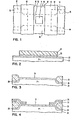
- FIG. 1 a prior art FET memory cell is shown.
- a border 10 is required around contact area 11 to assure the separation of the contact from the edges 12 of gate electrodes or word lines 13 and the edges 14 of field oxide regions 15.
- the edges 17 of electrodes 16 are also illustrated which are vertically separated from lines 13 by a dielectric layer.
- a FET inversion storage memory cell having a borderless contact is formed.
- a P-type monocrystalline silicon semiconductor substrate 21 Onto a P-type monocrystalline silicon semiconductor substrate 21 is formed a thermal silicon dioxide layer 23 of about 300 to 400 A in 0 thickness followed by a 1000 A thick layer 25 of chemical vapor deposited (CVD) silicon nitride.
- Silicon nitride layer 25 is patterned by standard lithography and etching techniques, using resist layer 27, to provide the structure shown in Fig. 2.
- a channel stop implant 28 is performed during which the resist layer 27 masks the boron implant.
- Resist layer 27 is stripped and field oxide regions 29 of about 6000 A in thickness are grown in steam at a temperature of about 1000°C.
- nitride layer 25 is stripped in hot phosphoric acid, oxide layer 23 is removed in buffered hydrofluoric acid and silicon dioxide layer 31 is grown in dry oxygen at a temperature of about 950°C to a thickness ° of about 500 A to produce the structure shown in Fig. 3.
- a CVD polysilicon layer 33 is then deposited over the struc- ° ture to a thickness of about 4000 A and a layer of phosphosilicate glass (PSG) is formed at the surface of layer 33 by an oxidation in an atmosphere of POC13.
- PSG phosphosilicate glass
- a CVD silicon dioxide layer 35 is then deposited to a thickness ° of about 3000 A and patterned using a resist layer and etching with buffered HF.
- the exposed portions of polysilicon layer 33 are then etched through the opening in. layer 35 by dry etching in a CF 4 + 0 2 plasma atmosphere or by wet etching with pyrocatechol to produce the structure of Fig. 4.
- the exposed portion of silicon dioxide layer 31 is etched through the opening in layer 33 with buffered HF and ° a 500 A thick gate silicon dioxide layer 37 is grown on the exposed surface of substrate 21 and also on the sidewalls 39 and top of polysilicon layer 33 (Fig. 5).
- a second layer of doped polysilicon, to provide gate electrodes 41, is formed and patterned by repeating the above steps with the polysilicon layer being .etched by reactive ion etching through overlying oxide layer 43 to give straight sidewalls as shown in Fig. 5.
- the portion of silicon dioxide layer 37 between gate electrodes 41 is then etched from the surface of substrate 21 and the resulting structure is reoxidized in steam 0 at a temperature of 800°C to grow 500 A of silicon dioxide on substrate 21 and 2000 A of silicon dioxide on the sidewalls 45 of the gate electrodes 41. This result is achieved due to the more rapid oxidation rate of the phosphorus doped polysilicon compared to the oxidation rate of the silicon substrate.
- the thin portion of this silicon dioxide layer is then removed from the surface portion 49 of the substrate while leaving at least about 1500 A of sidewall oxide 47 (Fig. 6) by using buffered HF or preferably by directional reactive ion etching in an atmosphere containing a mixture of CF 4 and hydrogen.
- a third polysilicon layer 51 having a thickness of 4000 to 8000 A is then blanket deposited by CVD and doped with phosphorus by oxidation in an atmosphere of POC1 3 followed by an anneal at a temperature of 950°C for 45 minutes in nitrogen.
- the anneal also diffuses phosphorous into the surface of substrate 21 to form a self-aligned N+ diffused region 53 which is in electrical contact with polysilicon layer 51 with the junction 52 being under the oxide layer 47 due to lateral diffusion of the phosphorus (Fig. 7).
- the function of the diffused region 53 in a Dennard type memory cell is to operate as the bit line in a memory cell array as is well known in the art.
- Layer 51 is then patterned by standard lithographic techniques and dry or wet etching.
- Thermal silicon dioxide layer 55 is next grown in steam at a temperature of 800°C.
- Contact hole 57 is opened through layer 55 to polysili.con layer 51 using a resist mask. The resist is stripped and a layer 59 of metal, such as aluminum is deposited and patterned to form the electrical connection to layer 51. Because the edge 50 of layer 51 overlaps the edges 40 of layer 41 and the edges 30 of the field oxide 29, the contact hole 57 can be misaligned so that it also overlaps layer 41 and field oxide 29 as shown in Fig. 9 without causing shorting of the contact to either the substrate or to the gate electrode.
- the contact structure of the invention is borderless in two dimensions. This results in a much more compact memory cell with the lithographic overlay tolerances being absorbed in the conductive polysilicon contact layer 51.
- the spacing between the edges of the gate electrodes and similarly the edges of the field oxide regions need be only about 2 pm rather than the 6 pm required previously to account for overlay tolerances.
- Figs. 10 and 11 illustrate alternate embodiments of the invention.
- the polysilicon contact- layer 51 can be used to connect adjacent bit diffusion N + regions 53 thus providing a polysilicon bit line in a memory array of cells of the type described, for example, by Dennard in U.S. Patent No. 3 387 286.
- the region can be formed by the ion implantation of arsenic or phosphorus after the growth of silicon dioxide layer 47 (Fig. 6) and the removal of this thin oxide from the surface 49 of substrate 21.
- a polysilicon or a metal layer 61 (Fig. 11) metal such as aluminum is then deposited to provide electrical contact to region 53.
Landscapes
- Engineering & Computer Science (AREA)
- Manufacturing & Machinery (AREA)
- Electrodes Of Semiconductors (AREA)
- Internal Circuitry In Semiconductor Integrated Circuit Devices (AREA)
- Semiconductor Memories (AREA)
Applications Claiming Priority (2)
| Application Number | Priority Date | Filing Date | Title |
|---|---|---|---|
| US182722 | 1980-08-29 | ||
| US06/182,722 US4409722A (en) | 1980-08-29 | 1980-08-29 | Borderless diffusion contact process and structure |
Publications (3)
| Publication Number | Publication Date |
|---|---|
| EP0046857A2 true EP0046857A2 (fr) | 1982-03-10 |
| EP0046857A3 EP0046857A3 (en) | 1982-09-08 |
| EP0046857B1 EP0046857B1 (fr) | 1985-02-13 |
Family
ID=22669728
Family Applications (1)
| Application Number | Title | Priority Date | Filing Date |
|---|---|---|---|
| EP81105495A Expired EP0046857B1 (fr) | 1980-08-29 | 1981-07-14 | Procédé de fabrication d'une structure de contact sans marge pour zones diffusées |
Country Status (4)
| Country | Link |
|---|---|
| US (1) | US4409722A (fr) |
| EP (1) | EP0046857B1 (fr) |
| JP (1) | JPS5750441A (fr) |
| DE (1) | DE3168886D1 (fr) |
Cited By (1)
| Publication number | Priority date | Publication date | Assignee | Title |
|---|---|---|---|---|
| EP0696060A3 (fr) * | 1994-08-04 | 1997-07-09 | Nec Corp | Procédé de fabrication d'un câblage et d'une structure de contact d'un dispositif semi-conducteur |
Families Citing this family (11)
| Publication number | Priority date | Publication date | Assignee | Title |
|---|---|---|---|---|
| JPS58209156A (ja) * | 1982-05-31 | 1983-12-06 | Nippon Telegr & Teleph Corp <Ntt> | 半導体装置の製造方法 |
| US4488348A (en) * | 1983-06-15 | 1984-12-18 | Hewlett-Packard Company | Method for making a self-aligned vertically stacked gate MOS device |
| JP2503621B2 (ja) * | 1989-01-23 | 1996-06-05 | 日本電気株式会社 | 半導体装置の製造方法 |
| US5541427A (en) * | 1993-12-03 | 1996-07-30 | International Business Machines Corporation | SRAM cell with capacitor |
| JP3396286B2 (ja) * | 1994-02-28 | 2003-04-14 | 三菱電機株式会社 | 半導体集積回路装置およびその製造方法 |
| US5641708A (en) * | 1994-06-07 | 1997-06-24 | Sgs-Thomson Microelectronics, Inc. | Method for fabricating conductive structures in integrated circuits |
| US5960318A (en) * | 1995-10-27 | 1999-09-28 | Siemens Aktiengesellschaft | Borderless contact etch process with sidewall spacer and selective isotropic etch process |
| US5792703A (en) * | 1996-03-20 | 1998-08-11 | International Business Machines Corporation | Self-aligned contact wiring process for SI devices |
| US5804485A (en) * | 1997-02-25 | 1998-09-08 | Miracle Technology Co Ltd | High density metal gate MOS fabrication process |
| US5970340A (en) | 1997-06-24 | 1999-10-19 | Micron Technology, Inc. | Method for making semiconductor device incorporating an electrical contact to an internal conductive layer |
| JP5339972B2 (ja) * | 2009-03-10 | 2013-11-13 | 株式会社ジャパンディスプレイ | 画像表示装置 |
Family Cites Families (12)
| Publication number | Priority date | Publication date | Assignee | Title |
|---|---|---|---|---|
| US3387286A (en) * | 1967-07-14 | 1968-06-04 | Ibm | Field-effect transistor memory |
| US3967981A (en) * | 1971-01-14 | 1976-07-06 | Shumpei Yamazaki | Method for manufacturing a semiconductor field effort transistor |
| US4074304A (en) * | 1974-10-04 | 1978-02-14 | Nippon Electric Company, Ltd. | Semiconductor device having a miniature junction area and process for fabricating same |
| JPS543480A (en) * | 1977-06-09 | 1979-01-11 | Fujitsu Ltd | Manufacture of semiconductor device |
| US4160991A (en) * | 1977-10-25 | 1979-07-10 | International Business Machines Corporation | High performance bipolar device and method for making same |
| US4251571A (en) * | 1978-05-02 | 1981-02-17 | International Business Machines Corporation | Method for forming semiconductor structure with improved isolation between two layers of polycrystalline silicon |
| US4157269A (en) * | 1978-06-06 | 1979-06-05 | International Business Machines Corporation | Utilizing polysilicon diffusion sources and special masking techniques |
| US4234362A (en) * | 1978-11-03 | 1980-11-18 | International Business Machines Corporation | Method for forming an insulator between layers of conductive material |
| US4240196A (en) * | 1978-12-29 | 1980-12-23 | Bell Telephone Laboratories, Incorporated | Fabrication of two-level polysilicon devices |
| CA1131796A (fr) * | 1979-01-08 | 1982-09-14 | Tarsaim L. Batra | Methode de fabrication de dispositif mos a contacts auto-alignes |
| JPS6055988B2 (ja) * | 1979-01-26 | 1985-12-07 | 株式会社日立製作所 | 半導体装置の製法 |
| JPS5650532A (en) * | 1979-10-01 | 1981-05-07 | Hitachi Ltd | Manufacture of semiconductor device |
-
1980
- 1980-08-29 US US06/182,722 patent/US4409722A/en not_active Expired - Lifetime
-
1981
- 1981-07-03 JP JP56103454A patent/JPS5750441A/ja active Granted
- 1981-07-14 EP EP81105495A patent/EP0046857B1/fr not_active Expired
- 1981-07-14 DE DE8181105495T patent/DE3168886D1/de not_active Expired
Cited By (1)
| Publication number | Priority date | Publication date | Assignee | Title |
|---|---|---|---|---|
| EP0696060A3 (fr) * | 1994-08-04 | 1997-07-09 | Nec Corp | Procédé de fabrication d'un câblage et d'une structure de contact d'un dispositif semi-conducteur |
Also Published As
| Publication number | Publication date |
|---|---|
| JPS5750441A (en) | 1982-03-24 |
| JPH0147020B2 (fr) | 1989-10-12 |
| DE3168886D1 (en) | 1985-03-28 |
| US4409722A (en) | 1983-10-18 |
| EP0046857A3 (en) | 1982-09-08 |
| EP0046857B1 (fr) | 1985-02-13 |
Similar Documents
| Publication | Publication Date | Title |
|---|---|---|
| US4803176A (en) | Integrated circuit structure with active device in merged slot and method of making same | |
| US4978629A (en) | Method of making a metal-oxide-semiconductor device having shallow source and drain diffused regions | |
| EP0088922B1 (fr) | Procédé pour fabriquer des électrodes et bandes d'interconnexion sur un dispositif semi-conducteur | |
| US4466172A (en) | Method for fabricating MOS device with self-aligned contacts | |
| US5545586A (en) | Method of making a transistor having easily controllable impurity profile | |
| US6852597B2 (en) | Method for fabricating power semiconductor device having trench gate structure | |
| US5270232A (en) | Process for fabricating field effect transistor | |
| EP0066081B1 (fr) | Transistor à effet de champ vertical à grande densité et procédé pour sa fabrication | |
| EP0164829A1 (fr) | Dispositif de mémoire à semi-conducteurs et procédé de fabrication | |
| US4374454A (en) | Method of manufacturing a semiconductor device | |
| US6534365B2 (en) | Method of fabricating TDMOS device using self-align technique | |
| KR100289474B1 (ko) | Dmos 트랜지스터를 제조하기 위한 방법 | |
| US4379001A (en) | Method of making semiconductor devices | |
| EP0162774B1 (fr) | Améliorations dans les procédés de fabrication d'une puce à circuit intégré et d'une puce réalisée selon ces procédés | |
| US4409722A (en) | Borderless diffusion contact process and structure | |
| KR870006673A (ko) | 자기정열된 쌍극성트랜지스터 구조의 제조공정 | |
| EP0009910A1 (fr) | Dispositif de mémoire à semiconducteurs et procédé de fabrication de ce dispositif | |
| EP0326211A1 (fr) | Dispositif semi-conducteur et procédé de fabrication de ce dispositif | |
| US4317690A (en) | Self-aligned double polysilicon MOS fabrication | |
| US4175317A (en) | Method for manufacturing junction type field-effect transistors | |
| KR920004366B1 (ko) | 반도체 장치의 자기 정렬 콘택 제조방법 | |
| US4219925A (en) | Method of manufacturing a device in a silicon wafer | |
| JPS5947468B2 (ja) | バイポ−ラ・トランジスタの製造方法 | |
| KR940003379B1 (ko) | 반도체장치의 제조방법 | |
| JPH05226655A (ja) | 半導体装置の製造方法 |
Legal Events
| Date | Code | Title | Description |
|---|---|---|---|
| PUAI | Public reference made under article 153(3) epc to a published international application that has entered the european phase |
Free format text: ORIGINAL CODE: 0009012 |
|
| 17P | Request for examination filed |
Effective date: 19811029 |
|
| AK | Designated contracting states |
Designated state(s): DE FR GB |
|
| PUAL | Search report despatched |
Free format text: ORIGINAL CODE: 0009013 |
|
| AK | Designated contracting states |
Designated state(s): DE FR GB |
|
| GRAA | (expected) grant |
Free format text: ORIGINAL CODE: 0009210 |
|
| AK | Designated contracting states |
Designated state(s): DE FR GB |
|
| REF | Corresponds to: |
Ref document number: 3168886 Country of ref document: DE Date of ref document: 19850328 |
|
| ET | Fr: translation filed | ||
| PLBE | No opposition filed within time limit |
Free format text: ORIGINAL CODE: 0009261 |
|
| STAA | Information on the status of an ep patent application or granted ep patent |
Free format text: STATUS: NO OPPOSITION FILED WITHIN TIME LIMIT |
|
| 26N | No opposition filed | ||
| PGFP | Annual fee paid to national office [announced via postgrant information from national office to epo] |
Ref country code: GB Payment date: 19910621 Year of fee payment: 11 |
|
| PGFP | Annual fee paid to national office [announced via postgrant information from national office to epo] |
Ref country code: FR Payment date: 19910625 Year of fee payment: 11 |
|
| PGFP | Annual fee paid to national office [announced via postgrant information from national office to epo] |
Ref country code: DE Payment date: 19910723 Year of fee payment: 11 |
|
| PG25 | Lapsed in a contracting state [announced via postgrant information from national office to epo] |
Ref country code: GB Effective date: 19920714 |
|
| GBPC | Gb: european patent ceased through non-payment of renewal fee |
Effective date: 19920714 |
|
| PG25 | Lapsed in a contracting state [announced via postgrant information from national office to epo] |
Ref country code: FR Effective date: 19930331 |
|
| PG25 | Lapsed in a contracting state [announced via postgrant information from national office to epo] |
Ref country code: DE Effective date: 19930401 |
|
| REG | Reference to a national code |
Ref country code: FR Ref legal event code: ST |