EP0047140A2 - Verfahren zum Umwandeln von Halbleiterzonen in monokristalline Zonen - Google Patents
Verfahren zum Umwandeln von Halbleiterzonen in monokristalline Zonen Download PDFInfo
- Publication number
- EP0047140A2 EP0047140A2 EP81303924A EP81303924A EP0047140A2 EP 0047140 A2 EP0047140 A2 EP 0047140A2 EP 81303924 A EP81303924 A EP 81303924A EP 81303924 A EP81303924 A EP 81303924A EP 0047140 A2 EP0047140 A2 EP 0047140A2
- Authority
- EP
- European Patent Office
- Prior art keywords
- optical energy
- providing
- areas
- area
- depositing
- Prior art date
- Legal status (The legal status is an assumption and is not a legal conclusion. Google has not performed a legal analysis and makes no representation as to the accuracy of the status listed.)
- Granted
Links
Images


Classifications
-
- H—ELECTRICITY
- H10—SEMICONDUCTOR DEVICES; ELECTRIC SOLID-STATE DEVICES NOT OTHERWISE PROVIDED FOR
- H10P—GENERIC PROCESSES OR APPARATUS FOR THE MANUFACTURE OR TREATMENT OF DEVICES COVERED BY CLASS H10
- H10P14/00—Formation of materials, e.g. in the shape of layers or pillars
- H10P14/20—Formation of materials, e.g. in the shape of layers or pillars of semiconductor materials
- H10P14/38—Formation of materials, e.g. in the shape of layers or pillars of semiconductor materials characterised by treatments done after the formation of the materials
- H10P14/3802—Crystallisation or recrystallisation of non-monocrystalline semiconductor materials, e.g. regrowth
- H10P14/3808—Crystallisation or recrystallisation of non-monocrystalline semiconductor materials, e.g. regrowth using laser beams
-
- H—ELECTRICITY
- H10—SEMICONDUCTOR DEVICES; ELECTRIC SOLID-STATE DEVICES NOT OTHERWISE PROVIDED FOR
- H10F—INORGANIC SEMICONDUCTOR DEVICES SENSITIVE TO INFRARED RADIATION, LIGHT, ELECTROMAGNETIC RADIATION OF SHORTER WAVELENGTH OR CORPUSCULAR RADIATION
- H10F71/00—Manufacture or treatment of devices covered by this subclass
- H10F71/131—Recrystallisation; Crystallization of amorphous or microcrystalline semiconductors
-
- H—ELECTRICITY
- H10—SEMICONDUCTOR DEVICES; ELECTRIC SOLID-STATE DEVICES NOT OTHERWISE PROVIDED FOR
- H10P—GENERIC PROCESSES OR APPARATUS FOR THE MANUFACTURE OR TREATMENT OF DEVICES COVERED BY CLASS H10
- H10P14/00—Formation of materials, e.g. in the shape of layers or pillars
- H10P14/20—Formation of materials, e.g. in the shape of layers or pillars of semiconductor materials
- H10P14/29—Formation of materials, e.g. in the shape of layers or pillars of semiconductor materials characterised by the substrates
- H10P14/2901—Materials
- H10P14/2922—Materials being non-crystalline insulating materials, e.g. glass or polymers
-
- H—ELECTRICITY
- H10—SEMICONDUCTOR DEVICES; ELECTRIC SOLID-STATE DEVICES NOT OTHERWISE PROVIDED FOR
- H10P—GENERIC PROCESSES OR APPARATUS FOR THE MANUFACTURE OR TREATMENT OF DEVICES COVERED BY CLASS H10
- H10P14/00—Formation of materials, e.g. in the shape of layers or pillars
- H10P14/20—Formation of materials, e.g. in the shape of layers or pillars of semiconductor materials
- H10P14/32—Formation of materials, e.g. in the shape of layers or pillars of semiconductor materials characterised by intermediate layers between substrates and deposited layers
- H10P14/3202—Materials thereof
- H10P14/3238—Materials thereof being insulating materials
-
- H—ELECTRICITY
- H10—SEMICONDUCTOR DEVICES; ELECTRIC SOLID-STATE DEVICES NOT OTHERWISE PROVIDED FOR
- H10P—GENERIC PROCESSES OR APPARATUS FOR THE MANUFACTURE OR TREATMENT OF DEVICES COVERED BY CLASS H10
- H10P14/00—Formation of materials, e.g. in the shape of layers or pillars
- H10P14/20—Formation of materials, e.g. in the shape of layers or pillars of semiconductor materials
- H10P14/32—Formation of materials, e.g. in the shape of layers or pillars of semiconductor materials characterised by intermediate layers between substrates and deposited layers
- H10P14/3242—Structure
- H10P14/3244—Layer structure
- H10P14/3251—Layer structure consisting of three or more layers
-
- H—ELECTRICITY
- H10—SEMICONDUCTOR DEVICES; ELECTRIC SOLID-STATE DEVICES NOT OTHERWISE PROVIDED FOR
- H10P—GENERIC PROCESSES OR APPARATUS FOR THE MANUFACTURE OR TREATMENT OF DEVICES COVERED BY CLASS H10
- H10P14/00—Formation of materials, e.g. in the shape of layers or pillars
- H10P14/20—Formation of materials, e.g. in the shape of layers or pillars of semiconductor materials
- H10P14/34—Deposited materials, e.g. layers
- H10P14/3402—Deposited materials, e.g. layers characterised by the chemical composition
- H10P14/3404—Deposited materials, e.g. layers characterised by the chemical composition being Group IVA materials
- H10P14/3411—Silicon, silicon germanium or germanium
-
- H—ELECTRICITY
- H10—SEMICONDUCTOR DEVICES; ELECTRIC SOLID-STATE DEVICES NOT OTHERWISE PROVIDED FOR
- H10P—GENERIC PROCESSES OR APPARATUS FOR THE MANUFACTURE OR TREATMENT OF DEVICES COVERED BY CLASS H10
- H10P14/00—Formation of materials, e.g. in the shape of layers or pillars
- H10P14/20—Formation of materials, e.g. in the shape of layers or pillars of semiconductor materials
- H10P14/34—Deposited materials, e.g. layers
- H10P14/3451—Structure
-
- H—ELECTRICITY
- H10—SEMICONDUCTOR DEVICES; ELECTRIC SOLID-STATE DEVICES NOT OTHERWISE PROVIDED FOR
- H10P—GENERIC PROCESSES OR APPARATUS FOR THE MANUFACTURE OR TREATMENT OF DEVICES COVERED BY CLASS H10
- H10P14/00—Formation of materials, e.g. in the shape of layers or pillars
- H10P14/20—Formation of materials, e.g. in the shape of layers or pillars of semiconductor materials
- H10P14/38—Formation of materials, e.g. in the shape of layers or pillars of semiconductor materials characterised by treatments done after the formation of the materials
- H10P14/3802—Crystallisation or recrystallisation of non-monocrystalline semiconductor materials, e.g. regrowth
- H10P14/3808—Crystallisation or recrystallisation of non-monocrystalline semiconductor materials, e.g. regrowth using laser beams
- H10P14/381—Beam shaping, e.g. using a mask
-
- H—ELECTRICITY
- H10—SEMICONDUCTOR DEVICES; ELECTRIC SOLID-STATE DEVICES NOT OTHERWISE PROVIDED FOR
- H10P—GENERIC PROCESSES OR APPARATUS FOR THE MANUFACTURE OR TREATMENT OF DEVICES COVERED BY CLASS H10
- H10P14/00—Formation of materials, e.g. in the shape of layers or pillars
- H10P14/20—Formation of materials, e.g. in the shape of layers or pillars of semiconductor materials
- H10P14/38—Formation of materials, e.g. in the shape of layers or pillars of semiconductor materials characterised by treatments done after the formation of the materials
- H10P14/3802—Crystallisation or recrystallisation of non-monocrystalline semiconductor materials, e.g. regrowth
- H10P14/382—Scanning of a beam
-
- H—ELECTRICITY
- H10—SEMICONDUCTOR DEVICES; ELECTRIC SOLID-STATE DEVICES NOT OTHERWISE PROVIDED FOR
- H10P—GENERIC PROCESSES OR APPARATUS FOR THE MANUFACTURE OR TREATMENT OF DEVICES COVERED BY CLASS H10
- H10P34/00—Irradiation with electromagnetic or particle radiation of wafers, substrates or parts of devices
- H10P34/40—Irradiation with electromagnetic or particle radiation of wafers, substrates or parts of devices with high-energy radiation
- H10P34/42—Irradiation with electromagnetic or particle radiation of wafers, substrates or parts of devices with high-energy radiation with electromagnetic radiation, e.g. laser annealing
-
- Y—GENERAL TAGGING OF NEW TECHNOLOGICAL DEVELOPMENTS; GENERAL TAGGING OF CROSS-SECTIONAL TECHNOLOGIES SPANNING OVER SEVERAL SECTIONS OF THE IPC; TECHNICAL SUBJECTS COVERED BY FORMER USPC CROSS-REFERENCE ART COLLECTIONS [XRACs] AND DIGESTS
- Y02—TECHNOLOGIES OR APPLICATIONS FOR MITIGATION OR ADAPTATION AGAINST CLIMATE CHANGE
- Y02E—REDUCTION OF GREENHOUSE GAS [GHG] EMISSIONS, RELATED TO ENERGY GENERATION, TRANSMISSION OR DISTRIBUTION
- Y02E10/00—Energy generation through renewable energy sources
- Y02E10/50—Photovoltaic [PV] energy
-
- Y—GENERAL TAGGING OF NEW TECHNOLOGICAL DEVELOPMENTS; GENERAL TAGGING OF CROSS-SECTIONAL TECHNOLOGIES SPANNING OVER SEVERAL SECTIONS OF THE IPC; TECHNICAL SUBJECTS COVERED BY FORMER USPC CROSS-REFERENCE ART COLLECTIONS [XRACs] AND DIGESTS
- Y02—TECHNOLOGIES OR APPLICATIONS FOR MITIGATION OR ADAPTATION AGAINST CLIMATE CHANGE
- Y02P—CLIMATE CHANGE MITIGATION TECHNOLOGIES IN THE PRODUCTION OR PROCESSING OF GOODS
- Y02P70/00—Climate change mitigation technologies in the production process for final industrial or consumer products
- Y02P70/50—Manufacturing or production processes characterised by the final manufactured product
-
- Y—GENERAL TAGGING OF NEW TECHNOLOGICAL DEVELOPMENTS; GENERAL TAGGING OF CROSS-SECTIONAL TECHNOLOGIES SPANNING OVER SEVERAL SECTIONS OF THE IPC; TECHNICAL SUBJECTS COVERED BY FORMER USPC CROSS-REFERENCE ART COLLECTIONS [XRACs] AND DIGESTS
- Y10—TECHNICAL SUBJECTS COVERED BY FORMER USPC
- Y10S—TECHNICAL SUBJECTS COVERED BY FORMER USPC CROSS-REFERENCE ART COLLECTIONS [XRACs] AND DIGESTS
- Y10S117/00—Single-crystal, oriented-crystal, and epitaxy growth processes; non-coating apparatus therefor
- Y10S117/903—Dendrite or web or cage technique
- Y10S117/904—Laser beam
Definitions
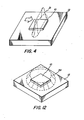
- the substrate will be hotter in the region of the lateral edges, resulting in a reduced rate of heat loss from the edges as compared to the central portion of the island.
- FIG. 9 An improved island configuration 10' is shown in Figure 9 wherein a tapered shape at the leading edge enhances self-seeding from a single point 38. This substantially eliminates the possibility of plural nucleation sites at the leading edge.
Landscapes
- Recrystallisation Techniques (AREA)
Applications Claiming Priority (2)
| Application Number | Priority Date | Filing Date | Title |
|---|---|---|---|
| US182195 | 1980-08-28 | ||
| US06/182,195 US4330363A (en) | 1980-08-28 | 1980-08-28 | Thermal gradient control for enhanced laser induced crystallization of predefined semiconductor areas |
Publications (3)
| Publication Number | Publication Date |
|---|---|
| EP0047140A2 true EP0047140A2 (de) | 1982-03-10 |
| EP0047140A3 EP0047140A3 (en) | 1984-10-17 |
| EP0047140B1 EP0047140B1 (de) | 1986-11-05 |
Family
ID=22667420
Family Applications (1)
| Application Number | Title | Priority Date | Filing Date |
|---|---|---|---|
| EP81303924A Expired EP0047140B1 (de) | 1980-08-28 | 1981-08-27 | Verfahren zum Umwandeln von Halbleiterzonen in monokristalline Zonen |
Country Status (5)
| Country | Link |
|---|---|
| US (1) | US4330363A (de) |
| EP (1) | EP0047140B1 (de) |
| JP (1) | JPS5772319A (de) |
| CA (1) | CA1157167A (de) |
| DE (1) | DE3175577D1 (de) |
Cited By (10)
| Publication number | Priority date | Publication date | Assignee | Title |
|---|---|---|---|---|
| EP0127323A1 (de) * | 1983-04-30 | 1984-12-05 | Fujitsu Limited | Verfahren zum Herstellen einer einkristallinen Halbleiterinsel auf einem Isolator |
| EP0154373A1 (de) * | 1984-02-21 | 1985-09-11 | Koninklijke Philips Electronics N.V. | Verfahren zum Herstellen von Einkristallen auf Isolatoren |
| EP0178447A3 (en) * | 1984-10-09 | 1988-02-03 | Fujitsu Limited | A manufacturing method of an integrated circuit based on the semiconductor-on-insulator technology and a device so manufactured |
| DE3921038A1 (de) * | 1988-06-28 | 1990-01-04 | Ricoh Kk | Halbleitersubstrat und verfahren zu dessen herstellung |
| US5173446A (en) * | 1988-06-28 | 1992-12-22 | Ricoh Company, Ltd. | Semiconductor substrate manufacturing by recrystallization using a cooling medium |
| US5310446A (en) * | 1990-01-10 | 1994-05-10 | Ricoh Company, Ltd. | Method for producing semiconductor film |
| US5459346A (en) * | 1988-06-28 | 1995-10-17 | Ricoh Co., Ltd. | Semiconductor substrate with electrical contact in groove |
| US7229861B2 (en) | 1994-09-16 | 2007-06-12 | Semiconductor Energy Laboratory Co., Ltd. | Method for producing semiconductor device |
| US7279372B2 (en) | 2001-12-11 | 2007-10-09 | Semiconductor Energy Laboratory Co., Ltd. | Manufacturing method of semiconductor device |
| US7393729B2 (en) | 2001-08-17 | 2008-07-01 | Semiconductor Energy Laboratory Co., Ltd. | Method for fabricating semiconductor device |
Families Citing this family (135)
| Publication number | Priority date | Publication date | Assignee | Title |
|---|---|---|---|---|
| US5302230A (en) * | 1980-02-27 | 1994-04-12 | Ricoh Company, Ltd. | Heat treatment by light irradiation |
| JPS5734331A (en) * | 1980-08-11 | 1982-02-24 | Toshiba Corp | Manufacture of semiconductor device |
| JPS58500048A (ja) * | 1981-02-04 | 1983-01-06 | ウエスタ−ン エレクトリツク カムパニ−,インコ−ポレ−テツド | 4族半導体材料を基礎とした構造の成長 |
| US4406709A (en) * | 1981-06-24 | 1983-09-27 | Bell Telephone Laboratories, Incorporated | Method of increasing the grain size of polycrystalline materials by directed energy-beams |
| JPS5821319A (ja) * | 1981-07-30 | 1983-02-08 | Fujitsu Ltd | レ−ザアニ−ル方法 |
| JPS5861622A (ja) * | 1981-10-09 | 1983-04-12 | Hitachi Ltd | 単結晶薄膜の製造方法 |
| US4388145A (en) * | 1981-10-29 | 1983-06-14 | Xerox Corporation | Laser annealing for growth of single crystal semiconductor areas |
| JPS58115832A (ja) * | 1981-12-28 | 1983-07-09 | Fujitsu Ltd | 半導体装置の製造方法 |
| JPS58164219A (ja) * | 1982-03-25 | 1983-09-29 | Agency Of Ind Science & Technol | 積層型半導体装置の製造方法 |
| JPS58194799A (ja) * | 1982-05-07 | 1983-11-12 | Hitachi Ltd | 単結晶シリコンの製造方法 |
| US4562106A (en) * | 1982-06-23 | 1985-12-31 | Massachusetts Institute Of Technology | Product made by method of entraining dislocations and other crystalline defects |
| US4479846A (en) * | 1982-06-23 | 1984-10-30 | Massachusetts Institute Of Technology | Method of entraining dislocations and other crystalline defects in heated film contacting patterned region |
| US4536231A (en) * | 1982-10-19 | 1985-08-20 | Harris Corporation | Polysilicon thin films of improved electrical uniformity |
| JPS59119718A (ja) * | 1982-12-27 | 1984-07-11 | Toshiba Corp | 薄膜単結晶の成長方法 |
| US4592799A (en) * | 1983-05-09 | 1986-06-03 | Sony Corporation | Method of recrystallizing a polycrystalline, amorphous or small grain material |
| JPS59229815A (ja) * | 1983-06-13 | 1984-12-24 | Hitachi Ltd | 半導体基板の製造方法 |
| US4853076A (en) * | 1983-12-29 | 1989-08-01 | Massachusetts Institute Of Technology | Semiconductor thin films |
| US4585512A (en) * | 1984-01-27 | 1986-04-29 | Sony Corporation | Method for making seed crystals for single-crystal semiconductor devices |
| JPS60213018A (ja) * | 1984-04-09 | 1985-10-25 | Hitachi Ltd | 半導体基板 |
| US4536251A (en) * | 1984-06-04 | 1985-08-20 | Xerox Corporation | Method for eliminating laser-induced substrate fissures associated with crystallized silicon areas |
| US4598305A (en) * | 1984-06-18 | 1986-07-01 | Xerox Corporation | Depletion mode thin film semiconductor photodetectors |
| US4737233A (en) * | 1984-10-22 | 1988-04-12 | American Telephone And Telegraph Company, At&T Bell Laboratories | Method for making semiconductor crystal films |
| US5753542A (en) * | 1985-08-02 | 1998-05-19 | Semiconductor Energy Laboratory Co., Ltd. | Method for crystallizing semiconductor material without exposing it to air |
| USRE33274E (en) * | 1985-09-13 | 1990-07-24 | Xerox Corporation | Selective disordering of well structures by laser annealing |
| US4654090A (en) * | 1985-09-13 | 1987-03-31 | Xerox Corporation | Selective disordering of well structures by laser annealing |
| JPH084067B2 (ja) * | 1985-10-07 | 1996-01-17 | 工業技術院長 | 半導体装置の製造方法 |
| EP0235819B1 (de) * | 1986-03-07 | 1992-06-10 | Iizuka, Kozo | Verfahren zum Herstellen einer monokristallinen Halbleiterschicht |
| US4771010A (en) * | 1986-11-21 | 1988-09-13 | Xerox Corporation | Energy beam induced layer disordering (EBILD) |
| US4743567A (en) * | 1987-08-11 | 1988-05-10 | North American Philips Corp. | Method of forming thin, defect-free, monocrystalline layers of semiconductor materials on insulators |
| US5453153A (en) * | 1987-11-13 | 1995-09-26 | Kopin Corporation | Zone-melting recrystallization process |
| US5021119A (en) * | 1987-11-13 | 1991-06-04 | Kopin Corporation | Zone-melting recrystallization process |
| US4885052A (en) * | 1987-11-13 | 1989-12-05 | Kopin Corporation | Zone-melting recrystallization process |
| US4888302A (en) * | 1987-11-25 | 1989-12-19 | North American Philips Corporation | Method of reduced stress recrystallization |
| JPH0633218B2 (ja) * | 1987-12-08 | 1994-05-02 | 日本鋼管株式会社 | シリコン単結晶の製造装置 |
| EP0459763B1 (de) * | 1990-05-29 | 1997-05-02 | Semiconductor Energy Laboratory Co., Ltd. | Dünnfilmtransistoren |
| JP3213338B2 (ja) * | 1991-05-15 | 2001-10-02 | 株式会社リコー | 薄膜半導体装置の製法 |
| US6975296B1 (en) * | 1991-06-14 | 2005-12-13 | Semiconductor Energy Laboratory Co., Ltd. | Electro-optical device and method of driving the same |
| US5329207A (en) * | 1992-05-13 | 1994-07-12 | Micron Technology, Inc. | Field emission structures produced on macro-grain polysilicon substrates |
| TW369686B (en) * | 1993-07-27 | 1999-09-11 | Semiconductor Energy Lab Corp | Semiconductor device and process for fabricating the same |
| US6884698B1 (en) | 1994-02-23 | 2005-04-26 | Semiconductor Energy Laboratory Co., Ltd. | Method for manufacturing semiconductor device with crystallization of amorphous silicon |
| KR100321541B1 (ko) | 1994-03-09 | 2002-06-20 | 야마자끼 순페이 | 능동 매트릭스 디스플레이 장치의 작동 방법 |
| US6723590B1 (en) * | 1994-03-09 | 2004-04-20 | Semiconductor Energy Laboratory Co., Ltd. | Method for laser-processing semiconductor device |
| TW280037B (en) * | 1994-04-22 | 1996-07-01 | Handotai Energy Kenkyusho Kk | Drive circuit of active matrix type display device and manufacturing method |
| JP3897826B2 (ja) * | 1994-08-19 | 2007-03-28 | 株式会社半導体エネルギー研究所 | アクティブマトリクス型の表示装置 |
| US5712191A (en) * | 1994-09-16 | 1998-01-27 | Semiconductor Energy Laboratory Co., Ltd. | Method for producing semiconductor device |
| JP3469337B2 (ja) * | 1994-12-16 | 2003-11-25 | 株式会社半導体エネルギー研究所 | 半導体装置の作製方法 |
| JP3778456B2 (ja) | 1995-02-21 | 2006-05-24 | 株式会社半導体エネルギー研究所 | 絶縁ゲイト型薄膜半導体装置の作製方法 |
| TW297138B (de) * | 1995-05-31 | 1997-02-01 | Handotai Energy Kenkyusho Kk | |
| US6790714B2 (en) * | 1995-07-03 | 2004-09-14 | Sanyo Electric Co., Ltd. | Semiconductor device, display device and method of fabricating the same |
| US6444506B1 (en) * | 1995-10-25 | 2002-09-03 | Semiconductor Energy Laboratory Co., Ltd. | Method of manufacturing silicon thin film devices using laser annealing in a hydrogen mixture gas followed by nitride formation |
| JP3870420B2 (ja) * | 1995-12-26 | 2007-01-17 | セイコーエプソン株式会社 | アクティブマトリクス基板の製造方法、エレクトロルミネッセンス装置の製造方法、表示装置の製造方法、及び電子機器の製造方法 |
| JP3729955B2 (ja) * | 1996-01-19 | 2005-12-21 | 株式会社半導体エネルギー研究所 | 半導体装置の作製方法 |
| JP3645380B2 (ja) | 1996-01-19 | 2005-05-11 | 株式会社半導体エネルギー研究所 | 半導体装置の作製方法、情報端末、ヘッドマウントディスプレイ、ナビゲーションシステム、携帯電話、ビデオカメラ、投射型表示装置 |
| US6478263B1 (en) * | 1997-01-17 | 2002-11-12 | Semiconductor Energy Laboratory Co., Ltd. | Semiconductor device and its manufacturing method |
| JP3645378B2 (ja) | 1996-01-19 | 2005-05-11 | 株式会社半導体エネルギー研究所 | 半導体装置の作製方法 |
| JP3645379B2 (ja) | 1996-01-19 | 2005-05-11 | 株式会社半導体エネルギー研究所 | 半導体装置の作製方法 |
| US5888858A (en) | 1996-01-20 | 1999-03-30 | Semiconductor Energy Laboratory Co., Ltd. | Semiconductor device and fabrication method thereof |
| US7056381B1 (en) | 1996-01-26 | 2006-06-06 | Semiconductor Energy Laboratory Co., Ltd. | Fabrication method of semiconductor device |
| US6180439B1 (en) * | 1996-01-26 | 2001-01-30 | Semiconductor Energy Laboratory Co., Ltd. | Method for fabricating a semiconductor device |
| US6465287B1 (en) | 1996-01-27 | 2002-10-15 | Semiconductor Energy Laboratory Co., Ltd. | Method for fabricating a semiconductor device using a metal catalyst and high temperature crystallization |
| US6100562A (en) | 1996-03-17 | 2000-08-08 | Semiconductor Energy Laboratory Co., Ltd. | Method of manufacturing a semiconductor device |
| US5893948A (en) * | 1996-04-05 | 1999-04-13 | Xerox Corporation | Method for forming single silicon crystals using nucleation sites |
| DE19651003C2 (de) * | 1996-11-29 | 2001-10-25 | Hahn Meitner Inst Berlin Gmbh | Verfahren zur Herstellung eines flächigen Einkristalls auf einem Fremdsubstrat |
| JP4112655B2 (ja) * | 1997-09-25 | 2008-07-02 | 東芝松下ディスプレイテクノロジー株式会社 | 多結晶薄膜の製造方法 |
| KR100269312B1 (ko) * | 1997-10-14 | 2000-10-16 | 윤종용 | 실리콘막의결정화방법및이를이용한박막트랜지스터-액정표시장치(tft-lcd)의제조방법 |
| JPH11214700A (ja) | 1998-01-23 | 1999-08-06 | Semiconductor Energy Lab Co Ltd | 半導体表示装置 |
| JPH11338439A (ja) | 1998-03-27 | 1999-12-10 | Semiconductor Energy Lab Co Ltd | 半導体表示装置の駆動回路および半導体表示装置 |
| JP3844613B2 (ja) | 1998-04-28 | 2006-11-15 | 株式会社半導体エネルギー研究所 | 薄膜トランジスタ回路およびそれを用いた表示装置 |
| GB9819338D0 (en) * | 1998-09-04 | 1998-10-28 | Philips Electronics Nv | Laser crystallisation of thin films |
| JP2000111950A (ja) * | 1998-10-06 | 2000-04-21 | Toshiba Corp | 多結晶シリコンの製造方法 |
| JP4748836B2 (ja) * | 1999-08-13 | 2011-08-17 | 株式会社半導体エネルギー研究所 | レーザ照射装置 |
| US6573162B2 (en) * | 1999-12-24 | 2003-06-03 | Semiconductor Energy Laboratory Co., Ltd. | Laser irradiation apparatus and method of fabricating a semiconductor device |
| US6780687B2 (en) * | 2000-01-28 | 2004-08-24 | Semiconductor Energy Laboratory Co., Ltd. | Method of manufacturing a semiconductor device having a heat absorbing layer |
| US6856630B2 (en) * | 2000-02-02 | 2005-02-15 | Semiconductor Energy Laboratory Co., Ltd. | Beam homogenizer, laser irradiation apparatus, semiconductor device, and method of fabricating the semiconductor device |
| US6872607B2 (en) * | 2000-03-21 | 2005-03-29 | Semiconductor Energy Laboratory Co., Ltd. | Method of manufacturing a semiconductor device |
| DE10042733A1 (de) * | 2000-08-31 | 2002-03-28 | Inst Physikalische Hochtech Ev | Multikristalline laserkristallisierte Silicium-Dünnschicht-Solarzelle auf transparentem Substrat |
| US6831299B2 (en) | 2000-11-09 | 2004-12-14 | Semiconductor Energy Laboratory Co., Ltd. | Semiconductor device |
| TWI313059B (de) * | 2000-12-08 | 2009-08-01 | Sony Corporatio | |
| SG113399A1 (en) * | 2000-12-27 | 2005-08-29 | Semiconductor Energy Lab | Laser annealing method and semiconductor device fabricating method |
| SG160191A1 (en) | 2001-02-28 | 2010-04-29 | Semiconductor Energy Lab | Semiconductor device and manufacturing method thereof |
| TW558861B (en) * | 2001-06-15 | 2003-10-21 | Semiconductor Energy Lab | Laser irradiation stage, laser irradiation optical system, laser irradiation apparatus, laser irradiation method, and method of manufacturing semiconductor device |
| US6692999B2 (en) * | 2001-06-26 | 2004-02-17 | Fujitsu Limited | Polysilicon film forming method |
| US6770546B2 (en) * | 2001-07-30 | 2004-08-03 | Semiconductor Energy Laboratory Co., Ltd. | Method of manufacturing semiconductor device |
| US6596077B2 (en) | 2001-07-31 | 2003-07-22 | Illinois Institute Of Technology | Controlled nucleation of protein crystals |
| US6733586B2 (en) | 2001-07-31 | 2004-05-11 | Illinois Institute Of Technology | High throughput non-photochemical laser induced nucleation |
| TW552645B (en) * | 2001-08-03 | 2003-09-11 | Semiconductor Energy Lab | Laser irradiating device, laser irradiating method and manufacturing method of semiconductor device |
| KR100885904B1 (ko) * | 2001-08-10 | 2009-02-26 | 가부시키가이샤 한도오따이 에네루기 켄큐쇼 | 레이저 어닐링장치 및 반도체장치의 제작방법 |
| TWI282126B (en) * | 2001-08-30 | 2007-06-01 | Semiconductor Energy Lab | Method for manufacturing semiconductor device |
| US7112517B2 (en) | 2001-09-10 | 2006-09-26 | Semiconductor Energy Laboratory Co., Ltd. | Laser treatment device, laser treatment method, and semiconductor device fabrication method |
| US7317205B2 (en) * | 2001-09-10 | 2008-01-08 | Semiconductor Energy Laboratory Co., Ltd. | Light emitting device and method of manufacturing a semiconductor device |
| JP4397571B2 (ja) | 2001-09-25 | 2010-01-13 | 株式会社半導体エネルギー研究所 | レーザ照射方法およびレーザ照射装置、並びに半導体装置の作製方法 |
| US6700096B2 (en) * | 2001-10-30 | 2004-03-02 | Semiconductor Energy Laboratory Co., Ltd. | Laser apparatus, laser irradiation method, manufacturing method for semiconductor device, semiconductor device, production system for semiconductor device using the laser apparatus, and electronic equipment |
| SG108878A1 (en) * | 2001-10-30 | 2005-02-28 | Semiconductor Energy Lab | Laser irradiation method and laser irradiation apparatus, and method for fabricating semiconductor device |
| TWI289896B (en) * | 2001-11-09 | 2007-11-11 | Semiconductor Energy Lab | Laser irradiation apparatus, laser irradiation method, and method of manufacturing a semiconductor device |
| JP3980465B2 (ja) * | 2001-11-09 | 2007-09-26 | 株式会社半導体エネルギー研究所 | 半導体装置の作製方法 |
| TWI291729B (en) | 2001-11-22 | 2007-12-21 | Semiconductor Energy Lab | A semiconductor fabricating apparatus |
| JP2003224070A (ja) * | 2001-11-26 | 2003-08-08 | Semiconductor Energy Lab Co Ltd | 半導体装置の作製方法 |
| US7105048B2 (en) * | 2001-11-30 | 2006-09-12 | Semiconductor Energy Laboratory Co., Ltd. | Laser irradiation apparatus |
| US7133737B2 (en) * | 2001-11-30 | 2006-11-07 | Semiconductor Energy Laboratory Co., Ltd. | Program for controlling laser apparatus and recording medium for recording program for controlling laser apparatus and capable of being read out by computer |
| US6979605B2 (en) * | 2001-11-30 | 2005-12-27 | Semiconductor Energy Laboratory Co., Ltd. | Manufacturing method for a semiconductor device using a marker on an amorphous semiconductor film to selectively crystallize a region with a laser light |
| JP3949564B2 (ja) * | 2001-11-30 | 2007-07-25 | 株式会社半導体エネルギー研究所 | レーザ照射装置及び半導体装置の作製方法 |
| US7214573B2 (en) * | 2001-12-11 | 2007-05-08 | Semiconductor Energy Laboratory Co., Ltd. | Method of manufacturing a semiconductor device that includes patterning sub-islands |
| US7135389B2 (en) * | 2001-12-20 | 2006-11-14 | Semiconductor Energy Laboratory Co., Ltd. | Irradiation method of laser beam |
| JP3992976B2 (ja) * | 2001-12-21 | 2007-10-17 | 株式会社半導体エネルギー研究所 | 半導体装置の作製方法 |
| JP4141138B2 (ja) * | 2001-12-21 | 2008-08-27 | 株式会社半導体エネルギー研究所 | 半導体装置の作製方法 |
| EP1326273B1 (de) * | 2001-12-28 | 2012-01-18 | Semiconductor Energy Laboratory Co., Ltd. | Halbleitervorrichtung |
| JP4011344B2 (ja) * | 2001-12-28 | 2007-11-21 | 株式会社半導体エネルギー研究所 | 半導体装置の作製方法 |
| JP4030758B2 (ja) * | 2001-12-28 | 2008-01-09 | 株式会社半導体エネルギー研究所 | 半導体装置の作製方法 |
| JP2003204067A (ja) * | 2001-12-28 | 2003-07-18 | Semiconductor Energy Lab Co Ltd | 表示装置およびそれを用いた電子機器 |
| US6933527B2 (en) | 2001-12-28 | 2005-08-23 | Semiconductor Energy Laboratory Co., Ltd. | Semiconductor device and semiconductor device production system |
| US6841797B2 (en) | 2002-01-17 | 2005-01-11 | Semiconductor Energy Laboratory Co., Ltd. | Semiconductor device formed over a surface with a drepession portion and a projection portion |
| US7749818B2 (en) * | 2002-01-28 | 2010-07-06 | Semiconductor Energy Laboratory Co., Ltd. | Semiconductor device and method of manufacturing the same |
| TW200302511A (en) * | 2002-01-28 | 2003-08-01 | Semiconductor Energy Lab | Semiconductor device and method of manufacturing the same |
| TWI261358B (en) * | 2002-01-28 | 2006-09-01 | Semiconductor Energy Lab | Semiconductor device and method of manufacturing the same |
| JP4137460B2 (ja) * | 2002-02-08 | 2008-08-20 | 株式会社半導体エネルギー研究所 | 半導体装置の作製方法 |
| KR100979926B1 (ko) * | 2002-03-05 | 2010-09-03 | 가부시키가이샤 한도오따이 에네루기 켄큐쇼 | 반도체소자 및 그것을 사용한 반도체장치 |
| US6847050B2 (en) * | 2002-03-15 | 2005-01-25 | Semiconductor Energy Laboratory Co., Ltd. | Semiconductor element and semiconductor device comprising the same |
| US6930326B2 (en) * | 2002-03-26 | 2005-08-16 | Semiconductor Energy Laboratory Co., Ltd. | Semiconductor circuit and method of fabricating the same |
| US6841434B2 (en) * | 2002-03-26 | 2005-01-11 | Semiconductor Energy Laboratory Co., Ltd. | Method of fabricating semiconductor device |
| US6984573B2 (en) * | 2002-06-14 | 2006-01-10 | Semiconductor Energy Laboratory Co., Ltd. | Laser irradiation method and apparatus |
| JP4532058B2 (ja) * | 2002-08-26 | 2010-08-25 | 日本発條株式会社 | 修正方法、修正装置及び修正プログラム |
| JP4282985B2 (ja) * | 2002-12-27 | 2009-06-24 | 株式会社半導体エネルギー研究所 | 表示装置の作製方法 |
| US7220627B2 (en) * | 2003-04-21 | 2007-05-22 | Semiconductor Energy Laboratory Co., Ltd. | Method for manufacturing a semiconductor device where the scanning direction changes between regions during crystallization and process |
| US7476629B2 (en) * | 2003-04-21 | 2009-01-13 | Semiconductor Energy Laboratory Co., Ltd. | Beam irradiation apparatus, beam irradiation method, and method for manufacturing thin film transistor |
| US7397592B2 (en) * | 2003-04-21 | 2008-07-08 | Semiconductor Energy Laboratory Co., Ltd. | Beam irradiation apparatus, beam irradiation method, and method for manufacturing a thin film transistor |
| TW594884B (en) * | 2003-05-29 | 2004-06-21 | Univ Nat Chiao Tung | Laser re-crystallization method of low temperature polysilicon thin film transistor |
| US7115449B2 (en) * | 2003-06-24 | 2006-10-03 | National Chiao Tung University | Method for fabrication of polycrystalline silicon thin film transistors |
| AU2004269196B2 (en) * | 2003-09-03 | 2010-03-04 | Shmuel Bukshpan | Methods and apparatus for rapid crystallization of biomolecules |
| JP2009135453A (ja) * | 2007-10-30 | 2009-06-18 | Semiconductor Energy Lab Co Ltd | 半導体装置の作製方法、半導体装置及び電子機器 |
| US8334194B2 (en) * | 2008-02-06 | 2012-12-18 | Motech Americas, Llc | Methods and apparatus for manufacturing semiconductor wafers |
| JP5091730B2 (ja) * | 2008-03-14 | 2012-12-05 | 株式会社日立製作所 | 薄膜半導体装置を用いた画像表示装置の製造方法 |
| US20090280336A1 (en) * | 2008-05-08 | 2009-11-12 | Ralf Jonczyk | Semiconductor sheets and methods of fabricating the same |
| US10115654B2 (en) | 2010-06-18 | 2018-10-30 | Palo Alto Research Center Incorporated | Buried thermally conductive layers for heat extraction and shielding |
| US9356171B2 (en) * | 2012-01-25 | 2016-05-31 | The Trustees Of Dartmouth College | Method of forming single-crystal semiconductor layers and photovaltaic cell thereon |
| US9065009B2 (en) | 2012-04-10 | 2015-06-23 | First Solar, Inc. | Apparatus and method for forming a transparent conductive oxide layer over a substrate using a laser |
Family Cites Families (8)
| Publication number | Priority date | Publication date | Assignee | Title |
|---|---|---|---|---|
| US3335038A (en) * | 1964-03-30 | 1967-08-08 | Ibm | Methods of producing single crystals on polycrystalline substrates and devices using same |
| US3348962A (en) * | 1964-08-13 | 1967-10-24 | Hughes Aircraft Co | Method and apparatus for preparing single crystal thin films |
| US3549432A (en) * | 1968-07-15 | 1970-12-22 | Texas Instruments Inc | Multilayer microelectronic circuitry techniques |
| US3585088A (en) * | 1968-10-18 | 1971-06-15 | Ibm | Methods of producing single crystals on supporting substrates |
| US3600237A (en) * | 1969-12-17 | 1971-08-17 | Us Navy | Controlled nucleation in zone recrystallized insb films |
| US3737739A (en) * | 1971-02-22 | 1973-06-05 | Ibm | Single crystal regions in dielectric substrate |
| US3764776A (en) * | 1972-02-28 | 1973-10-09 | Emerson Electric Co | Method of making coherent shape of silicon carbide |
| US4199397A (en) * | 1976-02-09 | 1980-04-22 | Motorola, Inc. | Spontaneous growth of large crystal semiconductor material by controlled melt perturbation |
-
1980
- 1980-08-28 US US06/182,195 patent/US4330363A/en not_active Expired - Lifetime
-
1981
- 1981-06-22 CA CA000380341A patent/CA1157167A/en not_active Expired
- 1981-08-20 JP JP56130836A patent/JPS5772319A/ja active Pending
- 1981-08-27 DE DE8181303924T patent/DE3175577D1/de not_active Expired
- 1981-08-27 EP EP81303924A patent/EP0047140B1/de not_active Expired
Non-Patent Citations (3)
| Title |
|---|
| APPLIED PHYSICS LETTERS, vol. 36, no. 11, 1st June 1980, pages 914-915, American Institute of Physics, New York, US; A.B. FOWLER et al.: "Selective laser annealing" * |
| APPLIED PHYSICS LETTERS, vol. 38, no. 3, 1st February 1981, pages 150-152, American Institute of Physics, New York, US; D.K. BIEGELSEN et al.: "Laser-induced crystallization of silicon islands on amorphous substrates: multilayer structures" * |
| IEEE TRANSACTIONS ON ELECTRON DEVICES, vol. ED-27, no. 3, March 1980, pages 573-578, IEEE, New York, US; G. YARON et al.: "LASOS-laser annealed silicon on sapphire" * |
Cited By (15)
| Publication number | Priority date | Publication date | Assignee | Title |
|---|---|---|---|---|
| US4543133A (en) * | 1983-04-30 | 1985-09-24 | Fujitsu Limited | Process for producing single crystalline semiconductor island on insulator |
| EP0127323A1 (de) * | 1983-04-30 | 1984-12-05 | Fujitsu Limited | Verfahren zum Herstellen einer einkristallinen Halbleiterinsel auf einem Isolator |
| EP0154373A1 (de) * | 1984-02-21 | 1985-09-11 | Koninklijke Philips Electronics N.V. | Verfahren zum Herstellen von Einkristallen auf Isolatoren |
| US5077233A (en) * | 1984-10-09 | 1991-12-31 | Fujitsu Limited | Method for recrystallizing specified portions of a non-crystalline semiconductor material to fabricate a semiconductor device therein |
| EP0178447A3 (en) * | 1984-10-09 | 1988-02-03 | Fujitsu Limited | A manufacturing method of an integrated circuit based on the semiconductor-on-insulator technology and a device so manufactured |
| US5173446A (en) * | 1988-06-28 | 1992-12-22 | Ricoh Company, Ltd. | Semiconductor substrate manufacturing by recrystallization using a cooling medium |
| DE3921038A1 (de) * | 1988-06-28 | 1990-01-04 | Ricoh Kk | Halbleitersubstrat und verfahren zu dessen herstellung |
| US5459346A (en) * | 1988-06-28 | 1995-10-17 | Ricoh Co., Ltd. | Semiconductor substrate with electrical contact in groove |
| US5565697A (en) * | 1988-06-28 | 1996-10-15 | Ricoh Company, Ltd. | Semiconductor structure having island forming grooves |
| DE3921038C2 (de) * | 1988-06-28 | 1998-12-10 | Ricoh Kk | Verfahren zur Herstellung eines Halbleitersubstrats bzw. Festkörperaufbaus |
| US5310446A (en) * | 1990-01-10 | 1994-05-10 | Ricoh Company, Ltd. | Method for producing semiconductor film |
| US7229861B2 (en) | 1994-09-16 | 2007-06-12 | Semiconductor Energy Laboratory Co., Ltd. | Method for producing semiconductor device |
| US7393729B2 (en) | 2001-08-17 | 2008-07-01 | Semiconductor Energy Laboratory Co., Ltd. | Method for fabricating semiconductor device |
| US7279372B2 (en) | 2001-12-11 | 2007-10-09 | Semiconductor Energy Laboratory Co., Ltd. | Manufacturing method of semiconductor device |
| US7670935B2 (en) | 2001-12-11 | 2010-03-02 | Semiconductor Energy Laboratory Co., Ltd. | Manufacturing method of semiconductor device |
Also Published As
| Publication number | Publication date |
|---|---|
| US4330363A (en) | 1982-05-18 |
| EP0047140B1 (de) | 1986-11-05 |
| JPS5772319A (en) | 1982-05-06 |
| DE3175577D1 (en) | 1986-12-11 |
| EP0047140A3 (en) | 1984-10-17 |
| CA1157167A (en) | 1983-11-15 |
Similar Documents
| Publication | Publication Date | Title |
|---|---|---|
| EP0047140B1 (de) | Verfahren zum Umwandeln von Halbleiterzonen in monokristalline Zonen | |
| EP0078681B1 (de) | Verfahren zur Herstellung von monokristallinen Halbleiterzonen | |
| US6322625B2 (en) | Crystallization processing of semiconductor film regions on a substrate, and devices made therewith | |
| US6756614B2 (en) | Thin film semiconductor device, polycrystalline semiconductor thin film production process and production apparatus | |
| US6169014B1 (en) | Laser crystallization of thin films | |
| EP0127323B1 (de) | Verfahren zum Herstellen einer einkristallinen Halbleiterinsel auf einem Isolator | |
| US4599133A (en) | Method of producing single-crystal silicon film | |
| JP2001274088A (ja) | 基板上の半導体膜領域の結晶化処理及びこの方法により製造されたデバイス | |
| EP0575965B1 (de) | Verfahren zur Herstellung eines Halbleiter-Kristalls und Halbleiteranordnung | |
| Biegelsen et al. | Laser induced crystal growth of silicon islands on amorphous substrates | |
| JP2993107B2 (ja) | 半導体薄膜の製造方法 | |
| JPH0236051B2 (de) | ||
| JPH0442358B2 (de) | ||
| JP2643204B2 (ja) | 単結晶薄膜の形成方法 | |
| JPS60191090A (ja) | 半導体装置の製造方法 | |
| JP2695462B2 (ja) | 結晶性半導体膜及びその形成方法 | |
| JPS62130509A (ja) | 半導体基体の製造方法 | |
| JPS60164318A (ja) | ビ−ムアニ−ル方法 | |
| JPS60236212A (ja) | 単結晶化方法 | |
| JPS58140113A (ja) | 結晶化法 | |
| JPS62272520A (ja) | 半導体基板の製造方法 |
Legal Events
| Date | Code | Title | Description |
|---|---|---|---|
| PUAI | Public reference made under article 153(3) epc to a published international application that has entered the european phase |
Free format text: ORIGINAL CODE: 0009012 |
|
| AK | Designated contracting states |
Designated state(s): DE FR GB IT NL |
|
| 17P | Request for examination filed |
Effective date: 19820716 |
|
| PUAL | Search report despatched |
Free format text: ORIGINAL CODE: 0009013 |
|
| AK | Designated contracting states |
Designated state(s): DE FR GB IT NL |
|
| 17Q | First examination report despatched |
Effective date: 19860121 |
|
| GRAA | (expected) grant |
Free format text: ORIGINAL CODE: 0009210 |
|
| AK | Designated contracting states |
Kind code of ref document: B1 Designated state(s): DE FR GB IT NL |
|
| REF | Corresponds to: |
Ref document number: 3175577 Country of ref document: DE Date of ref document: 19861211 |
|
| ET | Fr: translation filed | ||
| ITF | It: translation for a ep patent filed | ||
| PLBE | No opposition filed within time limit |
Free format text: ORIGINAL CODE: 0009261 |
|
| STAA | Information on the status of an ep patent application or granted ep patent |
Free format text: STATUS: NO OPPOSITION FILED WITHIN TIME LIMIT |
|
| 26N | No opposition filed | ||
| ITTA | It: last paid annual fee | ||
| PGFP | Annual fee paid to national office [announced via postgrant information from national office to epo] |
Ref country code: FR Payment date: 19980814 Year of fee payment: 18 |
|
| PGFP | Annual fee paid to national office [announced via postgrant information from national office to epo] |
Ref country code: GB Payment date: 19980818 Year of fee payment: 18 |
|
| PGFP | Annual fee paid to national office [announced via postgrant information from national office to epo] |
Ref country code: NL Payment date: 19980831 Year of fee payment: 18 |
|
| PGFP | Annual fee paid to national office [announced via postgrant information from national office to epo] |
Ref country code: DE Payment date: 19980907 Year of fee payment: 18 |
|
| PG25 | Lapsed in a contracting state [announced via postgrant information from national office to epo] |
Ref country code: GB Free format text: LAPSE BECAUSE OF NON-PAYMENT OF DUE FEES Effective date: 19990827 |
|
| PG25 | Lapsed in a contracting state [announced via postgrant information from national office to epo] |
Ref country code: NL Free format text: LAPSE BECAUSE OF NON-PAYMENT OF DUE FEES Effective date: 20000301 |
|
| GBPC | Gb: european patent ceased through non-payment of renewal fee |
Effective date: 19990827 |
|
| PG25 | Lapsed in a contracting state [announced via postgrant information from national office to epo] |
Ref country code: FR Free format text: LAPSE BECAUSE OF NON-PAYMENT OF DUE FEES Effective date: 20000428 |
|
| NLV4 | Nl: lapsed or anulled due to non-payment of the annual fee |
Effective date: 20000301 |
|
| PG25 | Lapsed in a contracting state [announced via postgrant information from national office to epo] |
Ref country code: DE Free format text: LAPSE BECAUSE OF NON-PAYMENT OF DUE FEES Effective date: 20000601 |
|
| REG | Reference to a national code |
Ref country code: FR Ref legal event code: ST |