EP0047320A1 - Circuit de linearisation et piece electronique de temporisation utilisant ce circuit - Google Patents
Circuit de linearisation et piece electronique de temporisation utilisant ce circuit Download PDFInfo
- Publication number
- EP0047320A1 EP0047320A1 EP81900075A EP81900075A EP0047320A1 EP 0047320 A1 EP0047320 A1 EP 0047320A1 EP 81900075 A EP81900075 A EP 81900075A EP 81900075 A EP81900075 A EP 81900075A EP 0047320 A1 EP0047320 A1 EP 0047320A1
- Authority
- EP
- European Patent Office
- Prior art keywords
- temperature
- frequency
- circuit
- pulses
- output
- Prior art date
- Legal status (The legal status is an assumption and is not a legal conclusion. Google has not performed a legal analysis and makes no representation as to the accuracy of the status listed.)
- Ceased
Links
Images


Classifications
-
- G—PHYSICS
- G04—HOROLOGY
- G04G—ELECTRONIC TIME-PIECES
- G04G3/00—Producing timing pulses
- G04G3/02—Circuits for deriving low frequency timing pulses from pulses of higher frequency
- G04G3/022—Circuits for deriving low frequency timing pulses from pulses of higher frequency the desired number of pulses per unit of time being obtained by adding to or substracting from a pulse train one or more pulses
-
- H—ELECTRICITY
- H03—ELECTRONIC CIRCUITRY
- H03L—AUTOMATIC CONTROL, STARTING, SYNCHRONISATION OR STABILISATION OF GENERATORS OF ELECTRONIC OSCILLATIONS OR PULSES
- H03L1/00—Stabilisation of generator output against variations of physical values, e.g. power supply
- H03L1/02—Stabilisation of generator output against variations of physical values, e.g. power supply against variations of temperature only
- H03L1/022—Stabilisation of generator output against variations of physical values, e.g. power supply against variations of temperature only by indirect stabilisation, i.e. by generating an electrical correction signal which is a function of the temperature
- H03L1/027—Stabilisation of generator output against variations of physical values, e.g. power supply against variations of temperature only by indirect stabilisation, i.e. by generating an electrical correction signal which is a function of the temperature by using frequency conversion means which is variable with temperature, e.g. mixer, frequency divider, pulse add/subtract logic circuit
Definitions
- the invention relates to a linearizer circuit which may be used to detect a physical quantity or parameter such as temperature by converting its change into a frequency, and also to an electronic watch which utilizes such linearizer circuit as temperature detecting means to provide a temeperature compensation.
- Conventional linearizing means may be categorized into two types, one in which the response of an element itself is made linear, and the other in whcih the response of the element is digitalized through an A/D conversion, which is then subjected to a linearization process.
- the former type may be exemplified by a combination of a temperature element, for example, a thermistor and a fixed resistor, which is connected in a bridge so that a linear output may be obtained in response to a temperature change. While a linear output response may be obtained with this arrangement, an increased number of additional components such as resistors is required, and also the circuit module increases its size, which is inconvenient for incorporation into an electronic watch, in particular. Additionally, variations in the operational response of the temperature detector circuit as well as of the additional components prevent an output response having a high stability and a high linearity from being obtained.
- the accuracy of an electronic watch has been drastically improved since the advent of a quartz oscillator which is used as a oscillator source.
- the quartz oscillator exhibits a temperaturefrequency response which is parabolic. This means that while the accuracy of the quartz watch remains stable in a temperature range which corresponds to the apex of the response, the accuracy is less than satisfactory in other temperature ranges. Accordingly, a number of compensation techniques have been proposed to compensate for the temperature repose of a quartz watch or a quartz oscillator.
- One of proposed temperature compensation techniques employs a capacitor which exhibits a complementary response to the parabolic temperature response of the quartz oscillator and which is connected in an oscillation loop to provide a compensation for the temperature response of the quartz oscillator.
- the accuracy of watch which can be achieved with this technique is limited because a capacitor having a temperature response which is perfectly complementary to that of the quartz oscillator is not available.
- the use of a capacitor suffers from disadvantages of an aging effect and an increased temperature hysteresis.
- a temperature sensor which has been used in the prior art at this end comprises a quartz oscillator exhibiting a different temperature response from that of a basic oscillator source.
- the principle of operation is based on deriving a beat signal between outputs from a reference or source oscillator and an oscillator circuit of a temperature sensor.
- quartz oscillators used to form the respective oscillators must have temperature responses which are in a given relationship. As a result, the choice and adjustment of these quartz oscillators and associated components such as capacitors represent a troublesome procedure, resulting in an increased cost and an increased power dissipation.
- ,It is a further object of the invention to provide an electronic watch in which a reference clock pulse is utilized to produce temperature information in a digital form, thereby enabling a temperature compensation of a high accuracy for the stepping rate while reducing external components required to such compensation to facilitate the integration and minimizing the power dissipation.
- the linearizer circuit of the invention comprises a frequency mixer for mixing at a given proportion a first - frequency which changes in accordance with a variation in a parameter such as temperature, voltage or the like, and a second frequency from a reference oscillator which does not depend on any parameter, and a derivation circuit which delivers an output pusle corresponding to an average period of the output signal from the mixer. In this manner, an output characteristic corresponding to a parameter is linearized in a digital manner.
- the described linearizer circuit is assembled into a clock or watch as means for detecting an environmental temperature for the watch.
- This means provides information relating to a temperature offset with respect to a reference temperature to enable a correction of a watch signal in accordance with the temperature offset.
- Fig. 1 shows a linearizer circuit of the invention which detects a change in a physical quantity being detected (such as temperature, voltage or the like, and hereafter referred to as a parameter) in terms of a frequency.
- a variable parameter-frequency sensor 1 (hereafter simply referred to as a sensor) having a nonlinear temperature response which is used to convert a change in a parameter to be sensed, for example, temperature, into a corresponding frequency.
- the sensor 1 delivers a first frequency f(x) which varies in accordance with a change in the parameter being detected, for example, temperature, and which is introduced into a frequency mizer 2.
- a second frequency f 0 which is produced by a reference oscillator 3 and which has no dependence upon - any parameter.
- the frequency mixer 2 functions to add or subtract the second frequency to or from the first frequency f(x) at a given proportion, and its output is fed to a derivation circuit 4 which produces a pulse having a width corresponding to the average period of an output from the frequency mixer 2.
- the frequency mixer 2 comprises an exclusive OR gate 2a as shown in Fig. 2.
- the derivation circuit 4 comprises a counter 4a, a differentiator 4b which differentiates a count-up signal from the counter, and an R-S flipflop 4c which is reset by an output from the differentiator 4b and which is set by a sampling pulse SP which is supplied at a given time interval.
- the Q output from the flipflop 4c is used to clear the counter 4a while the Q output is used as a control signal for operating the sensor 1 at a given time interval.
- the embodiment described above utilized the addition of the ffirst frequency f(x) and the second frequency f 0 . It will be noted that the addition occurs for ⁇ > 0 while the subtraction occurs for ⁇ 0 A beat circuit is used to form the frequency mixer 2 when the subtraction is desired.
- the condition in order for the linearity of the output characteristic be assured by eliminating the quadrature term is given by the following inequality: which indicates the extent of x for which the magnitude of the cubic term remains negligibly small as compared with the linear term.
- the sensor 1 may comprise an oscillator having a thermistor and a capacitor assembled therein.
- the effective range is (x) ⁇ 2
- the linearization of the output characteristic has been achieved by eliminating the quadrature term.
- a higher term may degrade the linearity of the output characteristic , and in such instance, it is also possible to eliminate such higher term. This can be done by providing a plurality of different proportions for mixing f(x) and f 0 so that a cubic and a higher order term may be eliminated.
- a linear output for a parameter being detected is produced in a digital manner by using only an output frequency from a reference oscillator which has a high precision. No external components are required, and also the implementation into an integrated circuit is facilitated.
- a linearizer circuit is provided which is simple in arrangement, and has a stable characteristic and a high flexibility andvhich can be easily incorporated into a watch or the like.
- FIG. 5 shows one embodiment of such electronic watch including an oscillator 10 which employs a quartz oscillator.
- a first frequency divider 11 divides the output frequency from the oscillator to produce pulses of 16 kHz, for example.
- a pulse insertion (or extract) circuit 12 is connected to the output of the frequency divider 11 for inserting (or extracting) a compensation pulse.
- the output from the pulse insertion circuit 12 is applied to a second frequency divider 13, which produces pulses having a period of one second.
- a counter unit 14 is adapted to receive the one second pulses from the frequency divider 13, and includes a "second", a minute, an hour and a day counter, the count of which is supplied through a display driver 15 to a display 16, thus indicating the time and the day in a digital manner.
- a temperature detector 17 is operable to convert a temperature offset from a reference temperature into a pulse train, which is supplied to an arithmetic circuit 18.
- the arithmetic circuit 18 operates to produce a number of pulses which is proportional to the square of a temperature change (due to the parabolic temperature response of the quartz oscillator) by operating upon the pulse train signal from the temperature detector 17.
- the pulses delivered by the arithmetic circuit 18 are fed to the pulse insertion circuit 12 within a given time interval to provide a temperature compensation.
- a timer 19 controls the operation / of the temperature sensor 17 and the arithmetic circuit 18, . and is adapted to be turned on and off periodically with a given time interval by the counter unit 14.
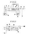
- Fig. 6 shows a specific circuit arrangement of the temperature detector 17.
- a linearizer circuit of the type mentioned above is indicated at 17b, and one of the input terminals of the exclusive OR gate 2a is connected to the output terminal of a pulse generator 17a having a nonlinear frequency variation with temperature, which may be implemented by utilizing a themistor or like element.
- the other input terminal of the gate 2a is connected to receive the signal from the crystal oscillator 10 shown in Fig. 5.
- the output terminal of the gate 2a is connected to an input terminal of the counter 4a, the output terminal of which is connected through the differentiator 4b to the reset terminal of the R-S flipflop 4c, all as mentioned previously.
- the Q output terminal of the flipflop 4c is connected to the clear or reset terminal of the counter 4a.
- the linearizer circuit 17b operates in a manner such that when a sampling pulse is applied to an input terminal IN to set the flipflop 4c, the counter 4a operates to count an output signal from the gate 2a, and when a given count is reached, it produces an output which is differentiated by the differentiator 4b to reset the flipflop 4c. In the manner mentioned previously, a pulse signal having a width which changes linearly with respect to the temperature is produced at the output terminal of the flipflop 4c.
- the temperature detector also comprises a reference pulse generator 17e which receives the sampling pulse from the input terminal IN at the same time as such pulse is applied to the linearizer circuit 17b. It produces a pulse signal of a width which is equal to the width of the pulse signal developed by the linearizer circuit 17b when the reference temperature TO prevails.
- An exclusive OR gate 17d receives the output from the linearizer circuit 17b and the output from the reference pulse generator 17e at" its both inputs, and operates to detect any difference therebetween.
- the output of the gate 17d enables an AND gate 17f, which passes a clock pulse CK of a frequency sufficiently higher than that of the sampling pulse, in accordance with the output from the gate 17d.
- Fig. 7 shows a specific example of the arithmetic circuit 18. It comprises an AND gate 18a having one of its inputs connected to receive the output signal from the temperature detector which is applied to an input terminal T 1 and its other input connected to receive the signal from the timer 19 which is applied to an input terminal T 3 , an NOR gate 18b having one of its inputs connected to receive the clock pulse which is applied to an input terminal T 2 and its other input connected to receive the timer signal from the input terminal T 3 , and OR gate 18c having its inputs connected to the outputs of NOR gate 18b and AND gate 18a, an up-down counter 18d which receives the output from OR gate 18c as an up or down input and counts up when the ouput from the timer 19 applied to the input terminal T 3 assumes an "H" level and counts down when the output assumes and "L” level, an R-S flipflop 18e having its set input connected to receive the output from the counter 18d when the count therein reaches zero and having its reset input - connected to the input terminal T 3
- a temperature detector generally exhibits a high temperature coefficient which may be as high as several %/degree if a thermistor or the like is used.
- a quartz oscillator which may be used as an oscillator source for a watch has a temperature coefficient which is on the order of ppm/degree and thus can be considered constant for temperature changes to which the temperature detector is exposed.
- the reference oscillation frequency or its frequency divided output may be directly used as "the second frequency from the reference oscillator which has no dependence upon any parameter" as used in the linearizer circuit of the invention.
- the exclusive OR gate 17d produces a signal, shown in Fig. 8D, which corresponds to the difference between the both pulses.
- the pulse width W is proportional to the magnitude (T - T 0
- a pulse train is developed at the output terminal OUT, as shown in Fig. 8E.
- the pulse train corresponds to the magnitude
- the number of output pulses N T produced during a single sampling is given by the following relationship: where ⁇ represents the clock pulse frequency. As shown in Fig. 9, the number of pulses N T is proportional to the temperature, and varies linearly on opposite sides of the normal temperature T 0 .
- the quartz oscillator used in the crystal oscillator has a parabolic temperature response as indicated by a curve II shown in Fig. 10 having an apex at the normal temperature T 0 (which represents a typical response of an X5°-cut oscillator in the form of a tuning fork which is most commonly used in wrist watches).
- the pulse train signal which is delivered by the temperature sensor 17 and applied to the input terminal T1 for each sampling operation is fed through AND gate 18f, which is enabled by the high level Q output from the flipflop 18e as shown in Fig. 11D, to be supplied to the output terminal OUT as shown in Fig. 11E.
- These output pulses are sequentially inserted into the insertion circuit 12 (Fig. 5) as correction pulses.
- the count in the counter 18d reaches zero, its output changes to an "H" level, whereby the flipflop 18e is set, inverting the Q output to its "L” level to terminate the insertion of the correction pulses into the circuit 12.
- the output from the timer 19 again changes to its "H" level, the above operation is repeated.
- the total number of pulses detected N which is outputted after the timer 19 is turned on is given as follows: assuming that there is no significant temperature change during one period of the timer. Such number of pulses may be directly inserted into the clock pulse train as described in the previous embodiment, or may be frequency divided before insertion. Where it is required to adjust for a different parabolic coefficient of the quartz oscillator, the frequency division, ratio or the period of the timer 19 may be changed. For example, if the frequency division ratio is reduced to one-half or the period of the timer is reduced to one-half its original value, the parabolic factor will be doubled.
- an input clock 9 to the reference pulse generator of Fig. 6 may be adjusted in accordance with the temperature TO of the quartz oscillator so that the pulse width becomes as close to ⁇ 0 as possible.
- a time constant circuit may be formed by a combination of a capacitor and a heat sensitive resistor which is formed by a parallel combination of a thermistor and a resistor so as to provide an improved temperature- resistance response, and the output of the time constant circuit may be connected to an inverter to provide a delay circuit having a time delay which depends on the temperature.
- Another delay circuit is provided which produces a given time delay irrespective of a temperature change to provide a version of the sampling pulse which is delayed by a given time interval independently from the temperature.
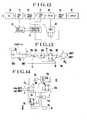
- Fig. 12 shows an electronic watch according to another embodiment of the invention.
- This embodiment includes an oscillator 10, a first frequency divider 11, a pulse insertion circuit 12, a second frequency divider 13, a counter 14, a driver 15 and a display 16, all of which are constructed and connected to each other in the same manner as shown in Fig. 5.
- a temperature detector 20 converts an offset ⁇ T from a reference temperature TO which may be 25°C, for example, into a corresponding number of pulses.
- a clock pulse formed by the first frequency divider 11 is introduced into the temperature detector 20, the output pulse of which is applied to a correction control circuit 21.
- the correction control circuit 21 operates, when the first sampling pulse SP from the second frequency divider 13 is introduced into it after a control signal S 1 from the timer 19 has been supplied thereto, to supply a correction control signal S 2 to the temperature detector 20 for counting output pulses therefrom.
- a number of insert pulses P 1 which are equal in number to the count are fed from the correction control circuit 21 into the insertion circuit 12 in timed relationship with the clock pulses.
- Fig. 13 shows a specific example of the temperature detector 20 and includes a variable temperature/frequency sensor 20a which converts a temperature change into a corresponding frequency.
- the sensor 20a comprises inverters INV1, INV2, thermistor R T , trimmer capacitor C T and fixed resistor r.
- the first frequency fx which depends on the temperature and which is produced by the sensor 20a is fed through NAND gate 20b to an exclusive OR gate 20c to be mixed therein with a reference frequency f0 derived from a desired frequency divider stage of the first frequency divider 11.
- Mix output pulses from the gate 20c are counted by a counter 20d, the count-up signal of which is applied to the reset input of an R-S flipflop 20e having its Q output connected to provide a clear signal to the counter 20d.
- the correction control signal S 2 produced by the correction control circuit 21 is applied to the set input S of the flipflop 20e, with its Q output being applied to the other input of NAND gate 20b and also applied to one input of an exclusive OR gate 20f.
- the other input of gate 20f receives a comparison signal S which is produced by the second frequency divider 13 so as to have a phase difference which prevails when the environment temperature T is equal to the reference temperature T 0 .
- NAND gate 20g The output from the gate 20f is applied as a gating input to NAND gate 20g, which also receives a frequency 2f 0 , namely, twice the reference frequency.
- NAND gate 20g -produces at its output terminal OUT1 a number of pulses which is proportional to a temperature offset from the reference temperature.
- Another terminal OUT2 is connected to the gate 20f for deriving a pulse of a width which is proportional to the magnitude of the temperature offset ⁇ T.
- Fig. 14 shows a specific example of the correction control circuit 21. Specifically, it comprises an up-down counter 21a which counts up pulses delivered at the output terminal OUT1 of the temperature detector 20 and counts down pulses from the terminal OUT2, an R-S flipflop 21b which is set by a zero detection pulse from the counter 21a and which is reset by the control signal S 1 from the timer 19, and a D-type flipflop 21c which is reset by the control signal S 1 from the timer 19 and which is clocked by the pulse from the terminal OUT2 of the temperature detector.
- An up count mode and a down count mode of the counter 21a are established in response to the Q output of the flipflop 20c which assumes a value of "1" and "0", respectively.
- the pulse from the terminal OUT1 of the temperature detector 20 is applied to the counter 21a through NAND gate 21d which is controlled by the Q output of the flipflop 21c and through NOR.gate 21e.
- the pulse from the terminal OUT2 of the temperature detector 20 is introduced into AND gate 21h which is enabled by the Q output from the flipflop 21c after passing through AND gate 21h, the pulse is supplied as an inserted output to the insertion circuit 12.
- the correction control signal which is supplied to the R-S flipflop 20e of the temperature detector 20 is derived from AND gate 21i which receives its inputs from the Q output of the flipflop 21b and the sampling pulse SP.
- the R-S flipflop 20e is set and reset each time the sampling pulse SP is applied to the correction control circuit 21, whereby a pulse is derived at the output . of the exclusive OR gate 20f or at the terminal OUT2 which has a width proportional to the temperature offset JT, as shown in Fig. 15c.
- a number of pulses N ( ⁇ T) which are proportional to the magnitude of ⁇ T (see Fig. 15d) is derived at the output of NAND gate 20g or at the terminal OUT1.
- These pulses N are fed throughNAND 21d and NOR gate 21e into the counter 21a, which then count them up. This count up operation takes place only when the initial sampling pulse SP is applied after the control signal S 1 from the timer has been produced. In the embodiment shown, the count is equal to "6".
- AND gate 21h of the correction control circuit 21 is enabled by the Q output of the flipflop 21c which assumes "1" level, so that the pulse'delivered to the output terminal OUT1 of the temperature detector for each sampling operation is supplied to the insertion circuit 12 as an inserted pulse P 1 (see Fig. 15h), which is inserted into the clock pulse train from the first frequency divider 11 with a proper timing.
- the total number of pulses which are supplied to the insertion circuit 12 through AND gate 21h in this manner is equal to the number of pulses P 1 delivered during a single sampling operation (which is equal to 6) multiplied by the number of sampling operations(equal to 6), or 6 2 , thus deriving a number of pulses which is equal to the square thereof.
- the equation (5) becomes equal to N 2 ( ⁇ T 0 ).
- N 2 ( ⁇ T 0 ) is multiplied by a small correction factor ⁇ N( ⁇ T)> /N( ⁇ T 0 ), thus providing an improved accuracy of the watch over the use of N 2 ( ⁇ T 0 ) alone.
- the insertion circuit 12 comprises an exclusive OR gate.
- the timing with which a pulse is inserted into the clock pulse train can be determined by delaying the count pulse from the temperature detector by one-half the period with respect to the clock pulses of the insertion stage.
- the temperature detector 20 may comprise a circuit arrangement as shown in Fig. 6, or may comprise a ring oscillator.
- the temperature response of the quartz oscillator may be compensated for in a manner mentioned below.
- the trimmer capacitor C T is adjusted to bring the value of TO of the temperature detector 20 into substantial coincidence with the apex temperature of the quartz oscillator.
- a number of pulses which are proportional to the square of the temperature offset ⁇ T is inserted into the clock pulse train, thereby compensating for the temperature response of the quartz oscillator.
- the degree of such compensation can be readily controlled by changing the period of the control signal S1 supplied by the timer 19 or by a suitable frequency division of the inserted pulses P 1 .
- the linearizer circuit of the invention can also be effectively used to provide a temperature compensation of a liquid display of multiplex drive type or electro-chromic display, or for linearization of a voltage, resistance or current output response.
Landscapes
- Physics & Mathematics (AREA)
- General Physics & Mathematics (AREA)
- Electric Clocks (AREA)
- Burglar Alarm Systems (AREA)
- Oscillators With Electromechanical Resonators (AREA)
- Dc Digital Transmission (AREA)
Abstract
Un circuit de linearisation comprend un circuit melangeur de frequences pour melanger selon un rapport predetermine, une premiere frequence variant en reponse a la variation d'un parametre avec une seconde frequence provenant d'une source d'oscillations de reference qui est independante du parametre, et un circuit arithmetique de production d'une impulsion de sortie correspondant a la periode moyenne de la sortie obtenue du circuit melangeur, de maniere a lineariser les caracteristiques de sortie du parametre. Ce circuit de linearisation est monte dans une piece electronique de temporisation et joue le role de moyen de detection de temperature ambiante, lesquels moyens detectent des informations de temperature pour corriger un signal d'horloge en fonction d'un changement de temperature par rapport a une temperature de reference, de maniere a compenser le changement de temperature.
Applications Claiming Priority (4)
| Application Number | Priority Date | Filing Date | Title |
|---|---|---|---|
| JP164680/79 | 1979-12-20 | ||
| JP16468079A JPS5687886A (en) | 1979-12-20 | 1979-12-20 | Electronic watch |
| JP91706/80 | 1980-07-07 | ||
| JP9170680A JPS5717812A (en) | 1980-07-07 | 1980-07-07 | Linearizing circuit |
Publications (2)
| Publication Number | Publication Date |
|---|---|
| EP0047320A1 true EP0047320A1 (fr) | 1982-03-17 |
| EP0047320A4 EP0047320A4 (fr) | 1982-05-10 |
Family
ID=26433150
Family Applications (1)
| Application Number | Title | Priority Date | Filing Date |
|---|---|---|---|
| EP19810900075 Ceased EP0047320A4 (fr) | 1979-12-20 | 1980-12-19 | Circuit de linearisation et piece electronique de temporisation utilisant ce circuit. |
Country Status (5)
| Country | Link |
|---|---|
| US (1) | US4464061A (fr) |
| EP (1) | EP0047320A4 (fr) |
| CH (1) | CH643979GA3 (fr) |
| GB (1) | GB2080579B (fr) |
| WO (1) | WO1981001888A1 (fr) |
Cited By (2)
| Publication number | Priority date | Publication date | Assignee | Title |
|---|---|---|---|---|
| FR2596932A1 (fr) * | 1986-04-04 | 1987-10-09 | Cepe | Procede de compensation en temperature d'un generateur de frequence et generateur de frequence pour la mise en oeuvre dudit procede |
| EP0711040A1 (fr) * | 1994-11-04 | 1996-05-08 | Asulab S.A. | Générateur de fréquence à haute stabilité |
Families Citing this family (11)
| Publication number | Priority date | Publication date | Assignee | Title |
|---|---|---|---|---|
| CH650122GA3 (fr) * | 1981-12-17 | 1985-07-15 | ||
| US4816752A (en) * | 1988-04-07 | 1989-03-28 | Snap-On Tools Corporation | Method and apparatus for low power offset correction of amplified sensor signals |
| US5327404A (en) * | 1990-11-27 | 1994-07-05 | Vlsi Technology, Inc. | On-chip frequency trimming method for real-time clock |
| US6086244A (en) * | 1997-03-20 | 2000-07-11 | Stmicroelectronics, Inc. | Low power, cost effective, temperature compensated, real time clock and method of clocking systems |
| US5917226A (en) | 1997-10-24 | 1999-06-29 | Stmicroelectronics, Inc. | Integrated released beam, thermo-mechanical sensor for sensing temperature variations and associated methods |
| US6028343A (en) | 1997-10-24 | 2000-02-22 | Stmicroelectronics, Inc. | Integrated released beam sensor for sensing acceleration and associated methods |
| US6058778A (en) | 1997-10-24 | 2000-05-09 | Stmicroelectronics, Inc. | Integrated sensor having plurality of released beams for sensing acceleration |
| US6124765A (en) * | 1997-10-24 | 2000-09-26 | Stmicroelectronics, Inc. | Integrated released beam oscillator and associated methods |
| JP3558040B2 (ja) * | 1999-03-30 | 2004-08-25 | セイコーエプソン株式会社 | 電子機器、電子機器の外部調整装置、電子機器の調整方法 |
| JP4862310B2 (ja) * | 2005-07-25 | 2012-01-25 | 富士ゼロックス株式会社 | 画像表示装置 |
| GB2448735A (en) * | 2007-04-26 | 2008-10-29 | Kevin John Richard Jones | Timepiece regulator |
Family Cites Families (14)
| Publication number | Priority date | Publication date | Assignee | Title |
|---|---|---|---|---|
| GB1383661A (en) * | 1971-04-30 | 1974-02-12 | Shinomura N | Temperature measuring equipment |
| US3713033A (en) * | 1971-09-01 | 1973-01-23 | Collins Radio Co | Digitally temperature compensated oscillator |
| JPS5071362A (fr) * | 1973-10-24 | 1975-06-13 | ||
| JPS52145675A (en) * | 1976-05-28 | 1977-12-03 | Sanyo Chemical Ind Ltd | Brake liquid having high boiling point |
| GB1570660A (en) * | 1976-06-30 | 1980-07-02 | Suwa Seikosha Kk | Electronic timepiece |
| JPS5388762A (en) * | 1976-12-27 | 1978-08-04 | Seiko Epson Corp | Electronic watch with temperature compensation |
| JPS6039192B2 (ja) * | 1977-05-25 | 1985-09-04 | セイコーエプソン株式会社 | 電子時計 |
| JPS5441773A (en) * | 1977-09-09 | 1979-04-03 | Seiko Instr & Electronics Ltd | Electronic watch |
| JPS5459173A (en) * | 1977-10-20 | 1979-05-12 | Ricoh Watch | Crystal watch temperature compensator |
| JPS5473671A (en) * | 1977-11-25 | 1979-06-13 | Seiko Epson Corp | Semiconductor integrated circuit for watch |
| US4160183A (en) * | 1978-05-26 | 1979-07-03 | Hewlett-Packard Company | Oscillator having a quartz resonator cut to compensate for static and dynamic thermal transients |
| JPS5576978A (en) * | 1978-12-05 | 1980-06-10 | Citizen Watch Co Ltd | Temperature compensating circuit for electronic watch |
| JPS5593306A (en) * | 1979-01-09 | 1980-07-15 | Citizen Watch Co Ltd | Crystal oscillation circuit |
| CH621680B (de) * | 1979-05-22 | Suisse Horlogerie | Oszillator mit temperaturkompensation. |
-
1980
- 1980-12-19 WO PCT/JP1980/000314 patent/WO1981001888A1/fr not_active Ceased
- 1980-12-19 CH CH536981A patent/CH643979GA3/de not_active IP Right Cessation
- 1980-12-19 EP EP19810900075 patent/EP0047320A4/fr not_active Ceased
- 1980-12-19 GB GB8125184A patent/GB2080579B/en not_active Expired
- 1980-12-19 US US06/293,223 patent/US4464061A/en not_active Expired - Fee Related
Cited By (4)
| Publication number | Priority date | Publication date | Assignee | Title |
|---|---|---|---|---|
| FR2596932A1 (fr) * | 1986-04-04 | 1987-10-09 | Cepe | Procede de compensation en temperature d'un generateur de frequence et generateur de frequence pour la mise en oeuvre dudit procede |
| EP0711040A1 (fr) * | 1994-11-04 | 1996-05-08 | Asulab S.A. | Générateur de fréquence à haute stabilité |
| FR2726705A1 (fr) * | 1994-11-04 | 1996-05-10 | Asulab Sa | Generateur de frequence a haute stabilite |
| US5719827A (en) * | 1994-11-04 | 1998-02-17 | Aulab S.A. | Highly stable frequency generator |
Also Published As
| Publication number | Publication date |
|---|---|
| US4464061A (en) | 1984-08-07 |
| WO1981001888A1 (fr) | 1981-07-09 |
| GB2080579A (en) | 1982-02-03 |
| EP0047320A4 (fr) | 1982-05-10 |
| CH643979B (de) | |
| GB2080579B (en) | 1984-10-10 |
| CH643979GA3 (en) | 1984-07-13 |
Similar Documents
| Publication | Publication Date | Title |
|---|---|---|
| US4464061A (en) | Linearizer circuit and an electronic watch incorporating same | |
| EP0147700B1 (fr) | Dispositif de compensation de température dans un système de traitement de données numérique | |
| US4453834A (en) | Electronic timepiece with temperature compensation | |
| HK41586A (en) | Thermometer | |
| US4473303A (en) | Electronic timepiece | |
| US4563748A (en) | Temperature measuring system | |
| US4370070A (en) | Digital thermometer having Fahrenheit and Celsius readout modes | |
| US4043109A (en) | Electronic timepiece | |
| US4844623A (en) | Electronic thermometer | |
| JPH06342088A (ja) | 計時方式、半導体装置、計時装置 | |
| US4779248A (en) | Electronic timepiece | |
| EP0511573A2 (fr) | Montre avec mémoire contenant les données pour ajuster l'horloger | |
| JPH0367209B2 (fr) | ||
| GB2327503A (en) | Device for measuring flow throughput of a flowing medium | |
| JP2504753B2 (ja) | 電子温度計 | |
| RU2017087C1 (ru) | Датчик температуры с частотным выходом | |
| SU1597559A1 (ru) | Устройство дл измерени суммарного расхода жидкостей и газов | |
| JPS6337225A (ja) | 温度検出回路 | |
| JPH0476074B2 (fr) | ||
| SU1224790A1 (ru) | Электронные часы | |
| JPS5868633A (ja) | 温度補償回路 | |
| SU1388815A1 (ru) | Измеритель сигналов датчика с низкочастотным выходом | |
| SU918884A1 (ru) | Цифровой фазометр-частотомер | |
| JP3180966B2 (ja) | デジタルヒステリシス回路 | |
| SU780169A1 (ru) | Генератор тактовых импульсов с программным управлением частотой следовани импульсов |
Legal Events
| Date | Code | Title | Description |
|---|---|---|---|
| PUAI | Public reference made under article 153(3) epc to a published international application that has entered the european phase |
Free format text: ORIGINAL CODE: 0009012 |
|
| AK | Designated contracting states |
Designated state(s): FR |
|
| 17P | Request for examination filed |
Effective date: 19820121 |
|
| STAA | Information on the status of an ep patent application or granted ep patent |
Free format text: STATUS: THE APPLICATION HAS BEEN REFUSED |
|
| 18R | Application refused |
Effective date: 19860711 |
|
| RIN1 | Information on inventor provided before grant (corrected) |
Inventor name: KAMIYA, KENJI |