EP0049624A1 - Imprimante à jet d'encre en mode d'opération binaire - Google Patents
Imprimante à jet d'encre en mode d'opération binaire Download PDFInfo
- Publication number
- EP0049624A1 EP0049624A1 EP81304581A EP81304581A EP0049624A1 EP 0049624 A1 EP0049624 A1 EP 0049624A1 EP 81304581 A EP81304581 A EP 81304581A EP 81304581 A EP81304581 A EP 81304581A EP 0049624 A1 EP0049624 A1 EP 0049624A1
- Authority
- EP
- European Patent Office
- Prior art keywords
- charging
- gutter
- drops
- electrodes
- Prior art date
- Legal status (The legal status is an assumption and is not a legal conclusion. Google has not performed a legal analysis and makes no representation as to the accuracy of the status listed.)
- Granted
Links
- 239000011159 matrix material Substances 0.000 claims abstract description 15
- 230000008878 coupling Effects 0.000 claims abstract description 11
- 238000010168 coupling process Methods 0.000 claims abstract description 11
- 238000005859 coupling reaction Methods 0.000 claims abstract description 11
- 239000007788 liquid Substances 0.000 claims description 12
- 238000005452 bending Methods 0.000 claims description 6
- 230000015572 biosynthetic process Effects 0.000 claims description 5
- 239000000758 substrate Substances 0.000 abstract description 26
- 239000002184 metal Substances 0.000 description 10
- 238000003491 array Methods 0.000 description 7
- 238000000034 method Methods 0.000 description 6
- 239000000126 substance Substances 0.000 description 6
- 239000004020 conductor Substances 0.000 description 5
- 239000011248 coating agent Substances 0.000 description 2
- 238000000576 coating method Methods 0.000 description 2
- 238000013461 design Methods 0.000 description 2
- 238000004519 manufacturing process Methods 0.000 description 2
- 239000000463 material Substances 0.000 description 2
- 238000012986 modification Methods 0.000 description 2
- 230000004048 modification Effects 0.000 description 2
- 125000006850 spacer group Chemical group 0.000 description 2
- 239000010409 thin film Substances 0.000 description 2
- 235000013290 Sagittaria latifolia Nutrition 0.000 description 1
- XUIMIQQOPSSXEZ-UHFFFAOYSA-N Silicon Chemical compound [Si] XUIMIQQOPSSXEZ-UHFFFAOYSA-N 0.000 description 1
- 230000004913 activation Effects 0.000 description 1
- 229910002056 binary alloy Inorganic materials 0.000 description 1
- 239000003990 capacitor Substances 0.000 description 1
- 235000015246 common arrowhead Nutrition 0.000 description 1
- 238000013329 compounding Methods 0.000 description 1
- 238000005520 cutting process Methods 0.000 description 1
- 230000003111 delayed effect Effects 0.000 description 1
- 238000009713 electroplating Methods 0.000 description 1
- 230000005686 electrostatic field Effects 0.000 description 1
- 230000008020 evaporation Effects 0.000 description 1
- 238000001704 evaporation Methods 0.000 description 1
- 239000010408 film Substances 0.000 description 1
- 230000003116 impacting effect Effects 0.000 description 1
- 238000003780 insertion Methods 0.000 description 1
- 230000037431 insertion Effects 0.000 description 1
- 238000012856 packing Methods 0.000 description 1
- 230000002093 peripheral effect Effects 0.000 description 1
- 230000008569 process Effects 0.000 description 1
- 238000004080 punching Methods 0.000 description 1
- 229910052710 silicon Inorganic materials 0.000 description 1
- 239000010703 silicon Substances 0.000 description 1
- 230000004936 stimulating effect Effects 0.000 description 1
- 230000000638 stimulation Effects 0.000 description 1
Images

Classifications
-
- B—PERFORMING OPERATIONS; TRANSPORTING
- B41—PRINTING; LINING MACHINES; TYPEWRITERS; STAMPS
- B41J—TYPEWRITERS; SELECTIVE PRINTING MECHANISMS, i.e. MECHANISMS PRINTING OTHERWISE THAN FROM A FORME; CORRECTION OF TYPOGRAPHICAL ERRORS
- B41J2/00—Typewriters or selective printing mechanisms characterised by the printing or marking process for which they are designed
- B41J2/005—Typewriters or selective printing mechanisms characterised by the printing or marking process for which they are designed characterised by bringing liquid or particles selectively into contact with a printing material
- B41J2/01—Ink jet
- B41J2/07—Ink jet characterised by jet control
- B41J2/075—Ink jet characterised by jet control for many-valued deflection
- B41J2/08—Ink jet characterised by jet control for many-valued deflection charge-control type
- B41J2/085—Charge means, e.g. electrodes
Definitions
- This invention relates to a binary ink drop printing apparatus wherein continuous streams of drops are generated from liquid emitted under pressure through a nozzle. Selected drops are electrostatically charged and deflected between flight paths intersecting either a target to be printed or a drop collection gutter.
- a binary printer is one wherein each nozzle supplies ink drops to cover a single point or pixel in a scan line of a raster pattern used to form an image on a target.
- An individual drop either goes to the pixel associated with its nozzle or a gutter.
- a print drop is charged to a print level to reach the target and is charged to a gutter level to intercept the gutter.
- a zero charge level may be the print level and some positive charge level of a significant non-zero magnitude may be the gutter level or vice versa.
- a multiple nozzle binary printer places a burden on the complexity of the wiring and electronic circuitry needed to electrically address a high number of nozzles.
- a rectangular raster pattern made up of scan lines having 3000 pixels or points requires a binary ink drop printer to have 3000 nozzles to cover each of the pixels.
- Each nozzle must be electrically addressed to set a drop to either of the binary charge levels: a print level or a gutter level.
- this requires that 3000 electrical connections be made to charging electrodes associated with each nozzle.
- Compounding the difficulty and complexity of such binary printers is that the nozzles are packed at a density of from about 20 to about 200 nozzles per centimeter (cm).
- U.S. Patents 3,373,437; 3,701,998; 3,984,843; 4,035,812 and 4,074,278.
- U.S. Patent 3,975,741 discloses a plural charge electrode structure suited for application in a binary printing system and specifically refers to U.S. 3,373,437 as an example of a binary system. None of these references disclose matrix addressing, two section charging electrodes, or a combination thereof.
- U.S. 3,701,998 in its Figure 2 (see in particular items 92, 94, 96 and 98) illustrates the numerous electrical connections required by prior art binary printers.
- U.S. Patent 4,074,278 discloses a charging electrode in aU-shape.
- the U-shaped electrode is merely a single section electrode.
- U.S. 4,035,812 discloses a current limiting resistor coupled to a charging electrode.
- U.S. 3,984,843 discloses a charging electrode array mounted on a silicon substrate. The substrate includes a shift register and latch circuit for coupling signals to the charge electrodes.
- the present invention is intended to provide a binary ink drop printing apparatus which is such as to reduce the complexity of electrically addressing a plurality of charging electrodes.
- the invention is characterised by M x N number of two section, drop charging means located at the region at which drops are created from a stream for charging print drops to a print level permitting them to reach a target for printing and for charging gutter drops to a gutter level permitting them to be collected by gutter means, and matrix means for coupling print and gutter voltages to the two sections fo the charging means to charge drops to either a print or a gutter level including M segment line means for coupling to one section of the charging means and N data line means for coupling to the other section of the charging means.
- a two section charging electrode is made by coupling two separate resistors to a charging electrode tunnel in a voltage divider arrangement. Like voltages applied to both ends of the divider network couple a potential to the tunnel equal to the applied voltage. A like voltage coupled to one end with the other end grounded, for example, couples a potential of half the magnitude (assuming a symmetrical divider) to the charging tunnel.
- the print voltage-for example ground potential- is simultaneously applied to both sections of the charging electrode to charge a drop to the print level.
- a gutter voltage-for example +50 volts- coupled to either or both sections of the charging electrode causes a drop to be charged to a gutter level proportional to either +25 or +50 volts.
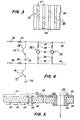
- the binary ink drop printer 1 of Figure 1 is of the type disclosed in U.S. patent 3,701,998 (see Figure 2) and in U.S. patent 4,035,812 (see Figures 2, 3 and 7).
- the printer 1 includes: a drop generator 2; the charging electrodes 3 and 4; the drop deflection electrodes 5, 6 and 7; the drop collection gutters 8 and 9; and the target 10 with the arrow 11 depicting the movement of the target relative to the apparatus 2-9.
- the member 12 is an electrically insulating substrate for supporting charging electrodes.
- the drop generator includes the chamber 14 containing a liquid ink 15 under pressure.
- the ink is emitted through nozzles 16 and 17 in continuous streams to the region of the charging electrodes 3 and 4 where the drops are formed.
- the formation of the drops at a fixed distance from the nozzles, the size of the drops and the spacing between drops is substantially constant due to a sonic stimulation of liquid 15 by a piezoelectric transducer (not shown) coupled to the chamber 14.
- the creation of uniform drop streams is also possible by mechanically vibrating the generator 2 or by electrohydro- dynamically stimulating the liquid as it leaves the nozzles.
- the liquid 15 is electrically grounded and drops formed from the liquid have a zero or near zero net charge. These uncharged or zero charge drops follow the undeflected trajectories indicated by dashed lines 18 and 19 to the target.
- the print drops are charged to a zero or near zero level by a ground or zero voltage coupled to the charging electrodes 3 and 4.
- Drops are also charged to a gutter level by the charging electrodes 3 and 4.
- a gutter voltage for example, +50 volts, is coupled to an electrode 3 or 4 at or just before the moment of drop formation to charge the drop to a non-zero level proportional to the 50 volts.
- the gutter drops are deflected by an electrostatic field established between deflection electrodes 5, 6 and 7 into one of the gutters 8 and 9.
- the gutter drops follow electrostatically deflected trajectories represented by the dashed lines 20 and 21.
- the nozzles 16 and 17 and the charging electrodes 3 and 4 are typical of a plurality of like nozzles and electrodes in two linear arrays.
- the specific electrodes 3 and 4 are single electrodes from the two arrays. Each array is offset by one pixel position to permit a closer packing of the nozzles and charging electrodes. Together the two arrays operate as if they were a single linear array with a number of nozzles equal to the combined number in the two linear arrays.
- the electrical data or video signals supplied to the second row of nozzles is delayed in time to allow the target 10 to move the distance separating the two arrays.
- a single scan line on the target is therefore formed from drops emitted by nozzles from both arrays.
- a single row or more than two rows of nozzles may be desirable for different printing systems.
- the present invention is directed toward method and apparatus for coupling print and gutter voltages to the electrodes 3 and 4.
- An improved printer is obtained by making a charging electrode with two sections and using a matrix network coupled to the two sections to address individual charge electrodes.
- FIG. 2 A matrix addressed, two section charging electrode array is shown in Figure 2. A single array of two section electrodes 25 are described for ease of discussion. Figure 3 illustrates the offset arrangement for electrodes 25 for use in the two rows of printer 1. One array or row is represented by charging electrodes 3 and the other by electrode 4 in Figure 1.
- the charging electrodes 25 shown in Figure 2 include voltage divider networks to form the two sections of the charging electrodes.
- this embodiment is also representative of other embodiments of a two section charging electrode as will be more apparent in connection with the discussion of Figures 6 through 9.
- the matrix concept for addressing the individual sections is discussed in connection with Figure 2.
- the electrodes 25 are supported by substrate 26 corresponding to substrate 12 in printer 1 of Figure 1.
- Each electrode 25 has upper and lower parallel connectors 27 and 28 electrically coupled to first and second sections of a charging electrode represented in this embodiment by thin film resistors 29 and 30.
- the connectors 27 and 28 are thin conductive metal strips formed on the top side of the substrate 26 by conventional printed circuit board techniques.
- segment input lines 32-35 are metal conductors formed on the bottom side of substrate 26.
- the lines 32-35 are generally orthogonal to conductors 27 and make electrical connection with the conductors 27 at the crossover locations indicated by the x's 38-41 at which metal through hole connectors 36 (shown in Figure 5) electrically couple lines 32-35 and lines 27 together.
- Segment line 32 is coupled to four adjacent connectors 27 by the four through holes 38 with lines 33, 34 and 35 being electrically connected to successive groups of four connectors 27 by the groups of four through holes 39, 40 and 41 respectively.
- the four parallel, data input lines 42-45 are thin film metal connectors formed on the bottom side of substrate 26.
- Lines 42-45 are orthogonal to the lower connectors 28 and are electrically coupled to them as indicated by the intersections marked by the x's 48-51.
- the data lines and connectors 28 are coupled by metal through hole connectors like through holes 36 for the segment lines and connectors 27 (shown in Figure 5).
- Data line 42 is coupled to the leftmost connector 28 and every fourth connector 27 to the right as indicated by the x's or through holes 48.
- data lines 43-45 are coupled to every fourth connector 28 by the groups of four through holes 49-51 respectively.
- the four segment and four data lines are electrically coupled to four-pin, board connectors 53 and 54 which in turn are coupled as represented by leads 55-56 to controller 57.
- the controller may be a microprocessor such as an Intel 8080 and appropriate peripheral devices or the like appropriately programmed to orchestrate all the operation of the printer 1.
- the controller contains all or a portion of the video signals or data to be recorded on target 10.
- the recording or printing occurs logically in a rectangular raster pattern made up of, for example, 4975 scan lines each having 3844 pixels. In the example under discussion, the numbers are reduced to sixteen pixels for ease of understanding.
- the 4 x 4 matrix of Figure 2 would be expanded to a 62 x 62 matrix to print the 3844 pixel scan line.
- the general case is an M x N matrix.
- two or more groups of matrices can be used in place of a single matrix. For example, two 31 x 62 matrices can be used in place of the single 62 x 62 matrix.
- An individual charging electrode is electrically addressed by controller 57 when a print voltage, for example zero volts, is simultaneously coupled to both sections of a two section charging electrode, i.e. to the upper and lower connectors 27 and 28 coupled to a specific electrode 25.
- the normal voltage level coupled to the segment lines 32-35 and the data lines 42-45 is the gutter voltage, for example + 50 volts. It follows therefore that the gutter voltage is normally coupled to both sections of all the two section electrodes via their connectors 27 and 28. All the drops charged during this period are charged to levels that cause the drops to follow trajectories such as paths 20 or 21. These gutter drops strike the deflection electrodes 5 or 7 (see Figure 1) and flow over the surfaces of those members into the cavities 8 and 9 defining the gutters.
- the momentum of the liquid impacting plates 5 and 7 and the surface tension of the liquid enables the liquid to flow along the vertical- surfaces of members 5 and 7, around their curved ends 23 and 24 and into the cavities or gutters 8 and 9.
- the trajectory followed by all gutter drops is not the same.
- the gutter is designed to catch gutter drops flying different paths.
- the printer 1 gutters represented by cavities 8 and 9 are an example of such a design but other gutter arrangements are possible at the choice of the designer.
- This reduced charge level is selected to still cause a drop to intersect a plate 5 or 7 (in Figure 1) and have the liquid flow into a cavity 8 or 9. Consequently, the lower charge level is still a gutter level and the drop is still properly referred to as a gutter drop.
- Controller 57 cyclically address the multiple electrodes 25 at a given clock rate.
- a print voltage is first applied to segment line 32 for nearly the entire clock period.
- the print voltage is sequentially applied to segment lines 33-35 respectively thereby defining a duty clock cycle.
- a print voltage is applied for a half-clock period sequentially to the four segment lines.
- a gutter voltage is coupled to the segment lines.
- the charging voltages are applied to the charging electrodes synchronously with the formation of the drops. See U.S. Patent 3,596,275 for a discussion of that operation.
- the charging electrodes coupled to segment line 32 are capable of generating print drops.
- the four adjacent charging electrodes to the far right are coupled via through holes 38 and upper connectors 27 to the segment line 32.
- the controller supplies print voltages in parallel to data lines 42-45 during this first clock period of a duty cycle according to the dictates of a given raster pattern image.
- a print voltage may appear on all four data lines42- 45 , none or some combination of less than all four lines according to the raster image.
- a print voltage being applied to both sections of an electrode 25 causes the creation of a print drop. This print drop travels to its assigned pixel location on target 10of printer 1.
- the data line for that pixel remains at the gutter potential.
- the gutter voltage coupled to the lower section prevents the generation of a print drop and insures that the drop is made a gutter drop.
- a print voltage on data line 42 during the first clock period of a duty cycle can not cause a print drop to be generated by the other charging electrodes to which it is coupled by through holes 48. The reason is that the upper sections of those electrodes are coupled to the gutter voltage at this time because only one segment line at a time is coupled to a print voltage.
- the remaining groups of electrodes 25 are capable of generating print drops in the same manner.
- the controller 57 keeps track of the segment line being addressed and applies print voltages to the data lines 42-45 in parallel according to the particulars of a given image being printed.
- An entire scan line is recorded during one duty cycle.
- the targetio is transported by appropriate means (not shown) relative to the nozzles to position the next scan line under the nozzles for the next adjacent scan line.
- the transport moves target 1 0 the distance separating trajectories 18 and 19 to align the drops into a single scan line on the target.
- a controller 57 in this case is programmed to apply half the video data associated with a scan line to charging electrodes 4 and thereafter the remaining half to electrodes 3.
- the voltage divider or resistive divider embodiment of a two section charging electrode may be understood by reference to Figures 2, 4 and 5 wherein like elements are assigned like reference numbers.
- the charging electrodes 25 of Figure 2 include a metal conductive cylinder or tunnel 62 and the resistors 29 and 30 electrically coupled to the tunnels.
- the tunnels have a diameter of from about two to four times that of a drop and ideally are aligned to the nozzles, such as 16 and 17 of a printer 1, so that a drop passes through it along its axis.
- the resistor 29 in electrical contact with tunnel 62 comprises a first section of the charging electrode and resistor 30 also in electrical contact with the tunnel comprises the second section of the charging electrode.
- a resistor 29 is coupled to an input segment line, for example line 32, via an upper connector 27 and a resistor 30 is coupled to an input data line, for example line 42, via a lower connector 28.
- the connections are typical for the other segment and data lines.
- the controller 57 includes (see Figure 4): a gutter voltage source represented by +V coupled to terminal 65 and 66; current limiting resistors 67 and 68 of three thousand ohms coupled to each segment line and data line; switches 70 and 71 coupled to the segment and data lines respectively; a print voltage source represented by the ground symbol coupled to the switches; and segment and data gate terminals 73 and 74.
- the switches are NPN transistors with their base electrodes coupled to the gate terminals 73 and 74, their collector electrodes coupled to the lines 32 and 42-for example-and their emitter electrodes coupled to the print voltage--e.g. ground 72.
- a gate signal applied to a gate 73 or 74 turns the transistor on thereby coupling the print voltage 72 to a segment or data line.
- the gate signals are applied to terminals 73 and 74 in the clocked manner described above. That is, a segment gate signal is applied to a terminal 73 during one clock period every duty cycle to partially activate the group of charging electrodes coupled to a particular segment line. Only one segment line at a time is coupled to the print voltage.
- Data gate signals are applied in parallel to all, none or some number of the data terminals 74 to fully activate the desired charging electrodes partially activated by a segment line. Activation means the generation of a print drop rather than of a gutter drop by a charging electrode.
- the charging tunnel 62 When the gutter voltage +V is coupled to lines 32 and 42, the charging tunnel 62 is at the + V gutter potential. When either line 32 or line 42 is coupled to the + V gutter potential and the other is coupled to the ground print potential, the voltage at the charging tunnel 62 is one-half +V for the case when the resistors 29 and 30 have the same value.
- the resistors 29 and 30 form a simple voltage divider network.
- the potential of a tunnel 62 is the print potential-ground-when the print voltage is simultaneously coupled to lines 32 and 42-for example.
- the board in Figure 2 is fabricated as indicated by Figure 5.
- the cylinders are hammered from both sides, i.e. riveted, to form the through holes 36 and charging tunnels 62.
- the through holes alternatively can be formed by an electroplating process.
- the top and bottom surfaces of substrate 26 are uniformly coated with a thin conductive metal by vapor evaporation in a vacuum.
- a photoresponsive chemical resist is coated over the conductive layers on both sides of the substrate.
- the top side of the substrate is exposed to a light pattern shaped to harden the resist in the regions corresponding to the shape of the upper and lower connectors 27 and 28.
- the bottom side of the substrate is exposed to a light pattern shaped to harden the resist in the regions corresponding to the shape of the segment and data input lines 32-35 and 42-45. Both sides of the substrate are then immersed into a chemical bath that removes the non- hardened resist and the underlying metal coating. Thereafter, the hardened resist is removed by an appropriate chemical bath.
- the resistors 29 and 30 are fabricated by coating the entire top side of substrate 26 including the connectors 27 and 28 with another photoresponsive chemical resist. This resist is exposed to a light pattern to harden the resist everywhere except in the regions corresponding to the resistors 29 and 30. The resist is then removed chemically in the regions corresponding to the resistors 29 and 30. At this stage, a resistive material is vacuum deposited onto the regions to be occupied by resistors 29 and 30. The excess resistive material is removed along with the chemical resist when the board is subjected to another appropriate chemical bath. Other known techniques for applying thick film resistors to circuit boards can also be used if desired.
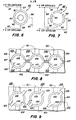
- FIGs 6-9 depict another embodiment of a two section charging electrode that can be substituted for the electrodes 25 in Figure 2.
- the two section charging electrode 80 includes the conductive metal half-cylinders 81 and 82.
- the two half-cylinders are the two sections of the charging electrode.
- An ink drop 83 is shown located at the center of the two sections 81 and 82.
- the ink 83 is electrically grounded, for example.
- the dashed line 84 represents the connection of the ink to a ground 85. This is conventionally done by grounding the generator 2 of Figure 2, for example.
- a gutter voltage of +V on a single section of an electrode, for example on line 32, induces charge in the grounded ink 83 that is determined by the expression Q VC.
- Q is the induced charge
- V is the potential difference between the ink 83 and the half-cylinder 81-+V in this example
- C is the capacitance of the structure which is directly proportional to the surface area of the half-cylinder 81.
- the induced charge is the desired gutter level making the drop a gutter drop.
- the preferred shape for a charging tunnel is cylindrical because a zero net bending force is exerted on the continuous stream of liquid and the emerging drop.
- the two half-cylinders provide two sections that approximate the symmetry of a full cylinder.
- Flat plates or other shapes can be used in place of the half-cylinders.
- the non-symmetrical bending forces can be compensated for by mechanical alignment of the nozzles to the target and by appropriate electrical biasing.
- FIG. 7 illustrates a two-section charging electrode 90 that maintains symmetry regardless whether a gutter voltage is applied to one or both sections of the electrode.
- Electrode 90 includes a first section made up of quarter-cylinders 91 and 92 and a second section made up of quarter-cylinders 93 and 94.
- the elements 91 and 92 and 93 and 94 are electrically coupled to each other by the conductors 95 and 96.
- the plate electrodes 91 and 92 When coupled to a +V potential-for example, the plate electrodes 91 and 92 subject ink at the center thereof (not shown in this figure) to a symmetrical charging potential. The same is true for plate electrodes 93 and 94.
- the ink in either case is not subjected to any meaningful bending force.
- the elements 91-94 can be flat plates or other shapes besides the preferred partial cylinder shapes. Also, symmetry is not always desired with either electrodes 80 or 90. A certain amount of non-symmetry to the charging field may be chosen to have gutter drops having two different charge levels follow closer trajectories to a gutter.
- FIGs 8 and 9 illustrate two different embodiments of the partial-cylinder or multiple element electrodes 80 and 90.
- the board 100 is like substrate 26 in Figure 2. It includes the upper and lower connectors 101 and 102 like connectors 27 and 28. Pre-punched (or otherwise formed) holes 103 are electroplated or the like to create conductive, cylindrical tunnels.
- the substrate 100 is then sawed into parts 105 and 106 along a line running through the centers of the holes 103. Thereafter, the substrate halves 105 and 106 are rejoined with the spacer elements 107 inserted as shown.
- the spacers are electrically insulating.
- the resultant structure gives rise to the two element, charging electrodes 108.
- the half-cylinders 109 and 110 comprise the first and second sections of these electrodes
- the substrate 120 and connectors 121 and 122 are also like substrate 26 and connectors 27 and 28 in Figure 2.
- Pre-punched (or otherwise formed) holes 123 are electroplated or the like to create conductive, cylindrical tunnels.
- the substrate 120 is then cut to form the square shaped holes 125 and 126 in the substrate 120.
- the square shape of holes 125 and 126 is selected for ease of illustration. These holes are formed by punching or broaching the substrate and the conductive tunnels with an arrow-head punch device inserted into the holes 123.
- the severed tunnels define the two section, charging electrode 128.
- the half-cylinders (or nearly so) 129 and 130 comprise the two sections of electrodes 128.
- one of the two gutter charge levels given to a gutter drop can be selected to be the print level.
- the charge levels associated with the ground potential and the other gutter charge level are the new gutter charge levels.
- different voltages besides ground potential can be coupled to the ink and other potentials besides that coupled to the ink can be used for the print voltage.
- the essential aspect here is that at least one unique combination of voltages applied to the two section electrode of this invnetion causes the generation of print drops and all others cause the generation of gutter drops.
Landscapes
- Particle Formation And Scattering Control In Inkjet Printers (AREA)
Applications Claiming Priority (2)
| Application Number | Priority Date | Filing Date | Title |
|---|---|---|---|
| US193558 | 1980-10-03 | ||
| US06/193,558 US4318111A (en) | 1980-10-03 | 1980-10-03 | Two section charging electrodes for binary ink drop printers |
Publications (2)
| Publication Number | Publication Date |
|---|---|
| EP0049624A1 true EP0049624A1 (fr) | 1982-04-14 |
| EP0049624B1 EP0049624B1 (fr) | 1985-06-26 |
Family
ID=22714123
Family Applications (1)
| Application Number | Title | Priority Date | Filing Date |
|---|---|---|---|
| EP81304581A Expired EP0049624B1 (fr) | 1980-10-03 | 1981-10-02 | Imprimante à jet d'encre en mode d'opération binaire |
Country Status (5)
| Country | Link |
|---|---|
| US (1) | US4318111A (fr) |
| EP (1) | EP0049624B1 (fr) |
| JP (1) | JPS5787968A (fr) |
| CA (1) | CA1168294A (fr) |
| DE (1) | DE3171133D1 (fr) |
Families Citing this family (4)
| Publication number | Priority date | Publication date | Assignee | Title |
|---|---|---|---|---|
| US4667207A (en) * | 1986-06-13 | 1987-05-19 | Burlington Industries, Inc. | Ink jet system catcher structure |
| FR2678549B1 (fr) * | 1991-07-05 | 1993-09-17 | Imaje | Procede et dispositif d'impression haute-resolution dans une imprimante a jet d'encre continu. |
| EP1074387A3 (fr) * | 1999-07-30 | 2003-01-15 | ATLANTIC ZEISER GmbH & Co. | Imprimante pour appareil d'impression par jet d'encre |
| CN106813694B (zh) * | 2016-12-21 | 2019-05-24 | 浙江众邦机电科技有限公司 | 一种无轴承编码器 |
Family Cites Families (7)
| Publication number | Priority date | Publication date | Assignee | Title |
|---|---|---|---|---|
| US3373437A (en) * | 1964-03-25 | 1968-03-12 | Richard G. Sweet | Fluid droplet recorder with a plurality of jets |
| US3701998A (en) * | 1971-10-14 | 1972-10-31 | Mead Corp | Twin row drop generator |
| US3984843A (en) * | 1974-07-01 | 1976-10-05 | International Business Machines Corporation | Recording apparatus having a semiconductor charge electrode |
| US3975741A (en) * | 1975-07-23 | 1976-08-17 | International Business Machines Corporation | Charge electrode for ink jet |
| US4035812A (en) * | 1976-07-12 | 1977-07-12 | The Mead Corporation | Ink jet recorder and charge ring plate therefor with reduced deplating current |
| US4074278A (en) * | 1976-12-22 | 1978-02-14 | The Mead Corporation | Compensation circuit for channel to channel crosstalk |
| US4274100A (en) * | 1978-04-10 | 1981-06-16 | Xerox Corporation | Electrostatic scanning ink jet system |
-
1980
- 1980-10-03 US US06/193,558 patent/US4318111A/en not_active Expired - Lifetime
-
1981
- 1981-08-20 CA CA000384321A patent/CA1168294A/fr not_active Expired
- 1981-09-24 JP JP56151334A patent/JPS5787968A/ja active Pending
- 1981-10-02 EP EP81304581A patent/EP0049624B1/fr not_active Expired
- 1981-10-02 DE DE8181304581T patent/DE3171133D1/de not_active Expired
Non-Patent Citations (2)
| Title |
|---|
| KEINE * |
| No relevant documents have been disclosed. * |
Also Published As
| Publication number | Publication date |
|---|---|
| EP0049624B1 (fr) | 1985-06-26 |
| DE3171133D1 (en) | 1985-08-01 |
| CA1168294A (fr) | 1984-05-29 |
| US4318111A (en) | 1982-03-02 |
| JPS5787968A (en) | 1982-06-01 |
Similar Documents
| Publication | Publication Date | Title |
|---|---|---|
| CA1204960A (fr) | Imprimante au jet d'encre | |
| US4122458A (en) | Ink jet printer having plural parallel deflection fields | |
| US4219822A (en) | Skewed ink jet printer with overlapping print lines | |
| US3718936A (en) | Electrostatic matrix head construction | |
| JPS5818231B2 (ja) | エキテキ ニヨル インサツ マタハ ヒフクホウホウ ト ソウチ | |
| US4274100A (en) | Electrostatic scanning ink jet system | |
| US4223320A (en) | Jet printer and electrode assembly therefor | |
| RU2141407C1 (ru) | Устройство для эжекции вещества и способ эжекции вещества | |
| US4085409A (en) | Method and apparatus for ink jet printing | |
| CA1165175A (fr) | Deflecteur de gouttes d'encre | |
| EP0049624B1 (fr) | Imprimante à jet d'encre en mode d'opération binaire | |
| EP0051448B1 (fr) | Appareil et méthode d'impression utilisant des gouttelettes liquides | |
| JPS5839674B2 (ja) | セイデンインサツヨウノデンキテキニ マドレスサレル アナアキヘンチヨウキ | |
| US4544930A (en) | Ink jet printer with secondary, cyclically varying deflection field | |
| US4314258A (en) | Ink jet printer including external deflection field | |
| US4307407A (en) | Ink jet printer with inclined rows of jet drop streams | |
| EP0753412B1 (fr) | Imprimante de projection de toner avec structure d'électrodes de commande améliorée | |
| US5159358A (en) | Divided screen printer | |
| US6003979A (en) | Gray scale printing with high resolution array ink jet | |
| JP3288279B2 (ja) | インクジェット記録装置 | |
| US4224523A (en) | Electrostatic lens for ink jets | |
| EP0780230A2 (fr) | Système de charge de gouttelettes pour imprimante à jet d'encre à haute résolution | |
| JP3264637B2 (ja) | インクジェット記録装置 | |
| EP0373889A2 (fr) | Source multiple pour la génération des particules chargées | |
| US4951071A (en) | Resistive nib ionographic imaging head |
Legal Events
| Date | Code | Title | Description |
|---|---|---|---|
| PUAI | Public reference made under article 153(3) epc to a published international application that has entered the european phase |
Free format text: ORIGINAL CODE: 0009012 |
|
| AK | Designated contracting states |
Designated state(s): DE GB IT |
|
| 17P | Request for examination filed |
Effective date: 19821004 |
|
| ITF | It: translation for a ep patent filed | ||
| GRAA | (expected) grant |
Free format text: ORIGINAL CODE: 0009210 |
|
| AK | Designated contracting states |
Designated state(s): DE GB IT |
|
| REF | Corresponds to: |
Ref document number: 3171133 Country of ref document: DE Date of ref document: 19850801 |
|
| PLBE | No opposition filed within time limit |
Free format text: ORIGINAL CODE: 0009261 |
|
| STAA | Information on the status of an ep patent application or granted ep patent |
Free format text: STATUS: NO OPPOSITION FILED WITHIN TIME LIMIT |
|
| 26N | No opposition filed | ||
| PGFP | Annual fee paid to national office [announced via postgrant information from national office to epo] |
Ref country code: GB Payment date: 19890930 Year of fee payment: 9 |
|
| PGFP | Annual fee paid to national office [announced via postgrant information from national office to epo] |
Ref country code: DE Payment date: 19891002 Year of fee payment: 9 |
|
| ITTA | It: last paid annual fee | ||
| PG25 | Lapsed in a contracting state [announced via postgrant information from national office to epo] |
Ref country code: GB Effective date: 19901002 |
|
| GBPC | Gb: european patent ceased through non-payment of renewal fee | ||
| PG25 | Lapsed in a contracting state [announced via postgrant information from national office to epo] |
Ref country code: DE Effective date: 19910702 |