EP0050132B1 - Supply apparatus - Google Patents
Supply apparatus Download PDFInfo
- Publication number
- EP0050132B1 EP0050132B1 EP81900980A EP81900980A EP0050132B1 EP 0050132 B1 EP0050132 B1 EP 0050132B1 EP 81900980 A EP81900980 A EP 81900980A EP 81900980 A EP81900980 A EP 81900980A EP 0050132 B1 EP0050132 B1 EP 0050132B1
- Authority
- EP
- European Patent Office
- Prior art keywords
- capacitor
- main transistor
- charge
- protective
- supply apparatus
- Prior art date
- Legal status (The legal status is an assumption and is not a legal conclusion. Google has not performed a legal analysis and makes no representation as to the accuracy of the status listed.)
- Expired
Links
- 239000003990 capacitor Substances 0.000 claims abstract description 72
- 230000001681 protective effect Effects 0.000 claims description 30
- 230000000903 blocking effect Effects 0.000 claims description 3
- 230000003111 delayed effect Effects 0.000 abstract 1
- 230000002441 reversible effect Effects 0.000 description 2
- 230000001934 delay Effects 0.000 description 1
- 238000000034 method Methods 0.000 description 1
- 238000012544 monitoring process Methods 0.000 description 1
- 230000000737 periodic effect Effects 0.000 description 1
- 230000009466 transformation Effects 0.000 description 1
Images
Classifications
-
- H—ELECTRICITY
- H05—ELECTRIC TECHNIQUES NOT OTHERWISE PROVIDED FOR
- H05B—ELECTRIC HEATING; ELECTRIC LIGHT SOURCES NOT OTHERWISE PROVIDED FOR; CIRCUIT ARRANGEMENTS FOR ELECTRIC LIGHT SOURCES, IN GENERAL
- H05B41/00—Circuit arrangements or apparatus for igniting or operating discharge lamps
- H05B41/14—Circuit arrangements
- H05B41/26—Circuit arrangements in which the lamp is fed by power derived from DC by means of a converter, e.g. by high-voltage DC
- H05B41/28—Circuit arrangements in which the lamp is fed by power derived from DC by means of a converter, e.g. by high-voltage DC using static converters
Definitions
- the invention relates to a power supply device according to the preamble of claim 1.
- a source of further losses is associated with the generation of the low operating voltages for the control electronics in power supply devices of the type mentioned at the outset, unless complex transformation circuits are used.
- the invention has for its object to reduce the power losses in a power supply device of the type mentioned with little circuitry.
- the protective capacitor thus forms, together with the charging capacitor, a capacitive voltage divider which, on the one hand, reduces the switch-off losses by delaying the voltage rise at the main transistor and with the aid of which it is possible to generate a low operating voltage on the charging capacitor with virtually no loss.
- the voltage supply for the electronics requires a higher positive and a smaller negative voltage.
- the charging capacitor of the auxiliary voltage source consists of two partial capacitors. It is not practical to adjust the relation of the voltages by appropriate selection of the capacitances, because then a very large capacitor would be needed to generate the lower voltage, but on the other hand the energy requirement is lower at the lower voltage level than at the higher one.
- the relation of the voltages at the two partial capacitors is therefore preferably set by appropriate dimensioning of the protective choke.
- the protective choke must be dimensioned approximately three times as large as would be necessary with a view to reducing the steepness of the discharge current of the protective capacitor; With capacitors of approximately the same capacitance, a voltage ratio of approximately 1: 3 can then be set.
- the charging capacitor receives energy from the DC voltage source. If the charging capacitor consists of two partial capacitors, one of them receives additional energy if the protective capacitor is charged when the main transistor is blocked.
- the protective capacitor is preferably dimensioned in such a way that this additional energy is at least sufficient to control the main transistor.
- the other partial capacitor is then charged with part of the energy of the protective capacitor through the protective inductor, which in turn charges the two partial capacitors in series connection, with the main transistor turned on.
- the energy supplied to the partial capacitors via the protective capacitor does not need to be supplied by the auxiliary voltage source, which can be dimensioned correspondingly smaller.
- the storage capacitor C18 feeds an inverter W and is connected on the one hand via a blocking inductor L1, the charging diode D27 and the charging inductor L4, and on the other hand via a measuring resistor R33 to a main rectifier G1 in a two-way circuit, which is fed by an AC voltage network N and essentially has one at its terminals provides unsmoothed voltage.
- the main transistor V6 via which the charging inductor L4 can be switched to the main rectifier and thus can be charged, is used to regulate the voltage at the storage capacitor C18.
- the signal at the measuring resistor R33 lying between the main transistor V6 and the storage capacitor C18 on the one hand and the main rectifier G1 on the other hand is fed via a delay element (resistor R27 and capacitor C14) to the input 7 of a control part with a controller X, which controls the main transistor V6 as a secondary switch.
- a swinging diode D42 is also connected in anti-parallel to the main transistor and the measuring resistor R33;
- the "invisible" capacitances (the choke, the diodes, etc.) can discharge past the main transistor V6 via these.
- the inductor L4 charges and the capacitor C14 decelerates until its voltage reaches the setpoint value which is fed to the controller X of the control part and takes the form of an unsmoothed rectified alternating voltage: the current drawn from the mains therefore has an average a sinusoidal course.
- the controller switches off the main transistor V6:
- the inductor L4 then outputs its energy via the charging diode D27 to the storage capacitor C18, the voltage of which in the meantime had dropped somewhat as a result of the load from the inverter W.
- the signal at the measuring resistor R33 and - with a delay - the signal at the capacitor C14 decrease.
- the delay element R27 / C14 is dimensioned such that the voltage at C14 reaches the lower switchover point of the regulator when the current through the charging inductor L4 has become zero, i.e. it has been completely magnetized back:
- V6 is then switched on, this transistor has to take over neither a residual current of the charging choke L4 nor a reverse current of the diode D27, so that practically no switch-on losses occur.
- the protective capacitor C17 serves to limit the voltage rise at the blocked main transistor V6 and is connected in parallel to the switching path of this transistor and the measuring resistor R33 via the decoupling diode D9 and a capacitor C8:
- the protective capacitor C17 charges via L4, D9 and a charging capacitor C8 and thereby delays the rise in the blocking voltage on the switching path of the main transistor V6, so that only a small power loss occurs.
- the DC operating voltages for the control section are supplied in the start-up phase by an additional rectifier G2 which is connected to the AC network N via capacitors C6, C7 and which feeds the partial capacitors C8 and C9 in series connection; the connection point of these two capacitors lies at the negative terminal of the main rectifier G1, so that they supply a positive or a negative operating voltage.
- the partial capacitor C8 is also connected to the main rectifier G1 via the decoupling diode D9, the protective capacitor C17 and the charging inductor L4 and thus receives an additional charge from the main rectifier when the main transistor V6 is blocked and C17 is charging; C17 is dimensioned with 300 pF so large that this additional charge of C8 is sufficient for the subsequent control of the main transistor. Additional rectifiers and capacitors C6, C7 are therefore only dimensioned for the remaining power requirements of the controller and monitoring section.
- the other partial capacitor C9 is connected via the protective inductor L9 and the protective capacitor C17 in parallel to the switching path of the main transistor V6 and the measuring resistor R33;
- the discharge current of the protective capacitor C17 flows through this discharge circuit and thus via C9 when the main transistor V6 is turned on, which in this case charges the partial capacitor C9.
- both capacitors have approximately the same capacitance (approx. 50 ⁇ f).
- the different voltages are set during operation by appropriate dimensioning of the protective choke L9: The latter is dimensioned about three times as large as would be necessary to sufficiently delay the rise in the discharge current from C17 to V6.
- the recharging of the partial capacitor C9 when the protective capacitor C17 is discharged via the main transistor V6 is namely considerably less than the charge of the partial capacitor C8 when the protective capacitor C17 is charged.
- Such a coordination of the time constants is assumed that a complete charge or discharge of C17 is guaranteed in the associated switching cycles of V6.
- the energy stored in the protective choke L9 is finally discharged via the diode D9 and the two partial capacitors C8 and C9 in series connection. This discharge process is irrelevant for the voltage relation across the partial capacitors, since it affects both capacitors to the same extent.
- the energy of the protective choke L9 is thus used to supply the electronics and does not burden the main transistor V6.
Landscapes
- Rectifiers (AREA)
- Circuit Arrangements For Discharge Lamps (AREA)
- Dc-Dc Converters (AREA)
Abstract
Description
Die Erfindung betrifft ein Stromversorgungsgerät gemäß Oberbegriff von Anspruch 1.The invention relates to a power supply device according to the preamble of claim 1.
Bei einem solchen Stromversorgungsgerät sind zwar die Ausschaltverluste des Haupttransistors reduziert, da dessen Sperrspannung wegen des Schutzkondensators nur verzögert ansteigt. Die periodische Entladung dieses Schutzkondensators bringt aber in der Regel wieder Verluste mit sich. Nur mit einer recht komplizierten Umschwingschaltung ist es bisher gelungen, diese Energie dem Verbraucher zuzuführen (ETZ Band 100, 1979, Heft 13, S. 664-670).In such a power supply device, the turn-off losses of the main transistor are reduced, since its reverse voltage rises only after a delay due to the protective capacitor. The periodic discharge of this protective capacitor usually results in losses. To date, this energy has only been able to be supplied to the consumer with a rather complicated switching circuit (ETZ Volume 100, 1979, Issue 13, pp. 664-670).
Eine Quelle weiterer Verluste ist bei Stromversorgungsgeräten der eingangs genannten Art mit der Erzeugung der niedrigen Betriebsspannungen für die Steuerelektronik verbunden, es sei denn, es würden aufwendige Transformationsschaltungen eingesetzt.A source of further losses is associated with the generation of the low operating voltages for the control electronics in power supply devices of the type mentioned at the outset, unless complex transformation circuits are used.
Der Erfindung liegt die Aufgabe zugrunde, die Leistungsverluste bei einem Stromversorgungsgerät der eingangs genannten Art bei geringem schaltungstechnischem Aufwand zu reduzieren.The invention has for its object to reduce the power losses in a power supply device of the type mentioned with little circuitry.
Die erfindungsgemäße Lösung dieser Aufgabe ist dabei durch die im Kennzeichen von Anspruch 1 angegebenen Merkmale charakterisiert.The solution to this problem according to the invention is characterized by the features specified in the characterizing part of claim 1.
Bei der Erfindung bildet somit der Schutzkondensator zusammen mit dem Ladekondensator einen kapazitiven Spannungsteiler, der einerseits die Ausschaltverluste durch Verzögerung des Spannungsanstieges an dem Haupttransistor reduziert und mit dessen Hilfe es gelingt, eine niedrige Betriebsspannung an dem Ladekondensator praktisch verlustlos zu erzeugen.In the invention, the protective capacitor thus forms, together with the charging capacitor, a capacitive voltage divider which, on the one hand, reduces the switch-off losses by delaying the voltage rise at the main transistor and with the aid of which it is possible to generate a low operating voltage on the charging capacitor with virtually no loss.
In vielen Fällen erfordert die Spannungsversorgung der Elektronik (Regler, Schutzeinrichtung) eine höhere positive und eine kleinere negative Spannung. Um diese zu erzeugen, besteht gemäß Weiterbildung der Erfindung der Ladekondensator der Hilfsspannungsquelle aus zwei Teilkondensatoren. Hierbei ist es unzweckmäßig, die Relation der Spannungen durch entsprechende Wahl der Kapazitäten einzustellen, da man dann gerade für die Erzeugung der niedrigeren Spannung einen sehr großen Kondensator benötigen würde, andererseits aber gerade der Energiebedarf auf dem niedrigeren Spannungsniveau geringer ist als auf dem höheren. Vorzugsweise wird daher die Relation der Spannungen an den beiden Teilkondensatoren durch entsprechende Bemessung der Schutzdrossel eingestellt. Die Schutzdrossel muß hierzu etwa dreimal so groß bemessen werden als es im Hinblick auf die Reduzierung der Steilheit des Entladestromes des Schutzkondensators erforderlich wäre; mit Kondensatoren etwa gleicher Kapazität läßt sich dann ein Spannungsverhältnis von etwa 1 : 3 einstellen.In many cases, the voltage supply for the electronics (controller, protective device) requires a higher positive and a smaller negative voltage. In order to generate this, the charging capacitor of the auxiliary voltage source consists of two partial capacitors. It is not practical to adjust the relation of the voltages by appropriate selection of the capacitances, because then a very large capacitor would be needed to generate the lower voltage, but on the other hand the energy requirement is lower at the lower voltage level than at the higher one. The relation of the voltages at the two partial capacitors is therefore preferably set by appropriate dimensioning of the protective choke. For this purpose, the protective choke must be dimensioned approximately three times as large as would be necessary with a view to reducing the steepness of the discharge current of the protective capacitor; With capacitors of approximately the same capacitance, a voltage ratio of approximately 1: 3 can then be set.
Bei der beschriebenen Weiterbildung der Erfindung erhält der Ladekondensator Energie von der Gleichspannungsquelle. Besteht der Ladekondensator aus zwei Teilkondensatoren, so erhält der eine davon eine Zusatzenergie, wenn der Schutzkondensator bei gesperrtem Haupttransistor aufgeladen wird. Der Schutzkondensator ist hierbei vorzugsweise so bemessen, daß diese Zusatzenergie wenigstens zur Durchsteuerung des Haupttransistors ausreicht. Der andere Teilkondensator wird dann bei durchgesteuertem Haupttransistor mit einem Teil der Energie des Schutzkondensators über die Schutzdrossel aufgeladen, die ihrerseits die beiden Teilkondensatoren in Reihenschaltung lädt. Die den Teilkondensatoren über den Schutzkondensator zugeführte Energie braucht die Hilfsspannungsquelle nicht zu liefern, die entsprechend kleiner bemessen werden kann. Besonders zweckmäßig ist es dabei, die Teilkondensatoren über einen Zusatzgleichrichter und über entsprechend klein bemessene Kondensatoren an das speisende Wechselspannungsnetz anzuschließen: Auf diese Weise lassen sich die niedrigen Betriebsgleichspannungen für die Elektronik des Steuerteiles nahezu verlustfrei auch dann erzeuger, wenn nur ein Wechselspannungsnetz mit verhältnismäßig hoher Spannung zur Verfügung steht.In the described development of the invention, the charging capacitor receives energy from the DC voltage source. If the charging capacitor consists of two partial capacitors, one of them receives additional energy if the protective capacitor is charged when the main transistor is blocked. The protective capacitor is preferably dimensioned in such a way that this additional energy is at least sufficient to control the main transistor. The other partial capacitor is then charged with part of the energy of the protective capacitor through the protective inductor, which in turn charges the two partial capacitors in series connection, with the main transistor turned on. The energy supplied to the partial capacitors via the protective capacitor does not need to be supplied by the auxiliary voltage source, which can be dimensioned correspondingly smaller. It is particularly useful to connect the partial capacitors to the supplying AC voltage network using an additional rectifier and correspondingly small capacitors: In this way, the low operating DC voltages for the electronics of the control section can be generated almost loss-free even if only an AC voltage network with a relatively high voltage is available.
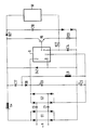
Ein Ausführungsbeispiel dieser Art wird anhand der Figur erläutert.An embodiment of this type is explained with reference to the figure.
Der Speicherkondensator C18 speist einen Wechselrichter W und ist einerseits über eine Sperrdrossel L1, die Ladediode D27 und die Ladedrossel L4, andererseits über einen Meßwiderstand R33 an einen Hauptgleichrichter G1 in Zweiwegschaltung angeschlossen, der von einem Wechselspannungsnetz N gespeist wird und an seinen Klemmen eine im wesentliche ungeglättete Spannung liefert.The storage capacitor C18 feeds an inverter W and is connected on the one hand via a blocking inductor L1, the charging diode D27 and the charging inductor L4, and on the other hand via a measuring resistor R33 to a main rectifier G1 in a two-way circuit, which is fed by an AC voltage network N and essentially has one at its terminals provides unsmoothed voltage.
Zur Regelung der Spannung an dem Speicherkondensator C18 dient der Haupttransistor V6, über den die Ladedrossel L4 an den Hauptgleichrichter schaltbar und dadurch aufladbar ist. Das Signal an dem zwischen Haupttransistor V6 und Speicherkondensator C18 einerseits und Hauptgleichrichter G1 andererseits liegenden Meßwiderstand R33 wird über ein Verzögerungsglied (Widerstand R27 und Kondensator C14) dem Eingang 7 eines Steuerteiles mit einem Regler X zugeführt, der den Haupttransistor V6 als Sctialter steuert.The main transistor V6, via which the charging inductor L4 can be switched to the main rectifier and thus can be charged, is used to regulate the voltage at the storage capacitor C18. The signal at the measuring resistor R33 lying between the main transistor V6 and the storage capacitor C18 on the one hand and the main rectifier G1 on the other hand is fed via a delay element (resistor R27 and capacitor C14) to the input 7 of a control part with a controller X, which controls the main transistor V6 as a secondary switch.
Dem Haupttransistor und dem Meßwiderstand R33 ist ferner eine Umschwingdiode D42 antiparallel geschaltet; über diese können sich die »unsichtbaren« Kapazitäten (der Drossel, der Dioden, etc.) am Haupttransistor V6 vorbei entladen.A swinging diode D42 is also connected in anti-parallel to the main transistor and the measuring resistor R33; The "invisible" capacitances (the choke, the diodes, etc.) can discharge past the main transistor V6 via these.
Bei durchgesteuertem Haupttransistor V6 lädt sich die Drossel L4 und verzögert der Kondensator C14 auf, bis dessen Spannung den Sollwert erreicht, der dem Regler X des Steuerteiles zugeführt wird und die Form einer ungeglätteten gleichgerichteten Wechselspannung hat: Der aus dem Netz gezogene Strom hat somit im Mittel einen sinusförmigen Verlauf.When the main transistor V6 is turned on, the inductor L4 charges and the capacitor C14 decelerates until its voltage reaches the setpoint value which is fed to the controller X of the control part and takes the form of an unsmoothed rectified alternating voltage: the current drawn from the mains therefore has an average a sinusoidal course.
Sobald der Istwert den Sollwert erreicht hat, schaltet der Regler den Haupttransistor V6 ab: Die Drossel L4 gibt dann ihre Energie über die Ladediode D27 an den Speicherkondensator C18 ab, dessen Spannung in der Zwischenzeit infolge der Belastung durch den Wechselrichter W etwas abgesunken war. Während der Aufladung des Speicherkondensators nimmt das Signal am Meßwiderstand R33 und - verzögert - das Signal am Kondensator C14 ab. Das Verzögerungsglied R27/C14 ist so bemessen, daß die Spannung an C14 gerade dann den unteren Umschaltpunkt des Reglers erreicht, wenn der Strom durch die Ladedrossel L4 Null geworden, diese also vollständig rückmagnetisiert ist: Bei der dann folgenden Einschaltung von V6 hat dieser Transistor somit weder einen Reststrom der Ladedrossel L4 noch einen Rückstrom der Diode D27 zu übernehmen, so daß praktisch keine Einschaltverluste entstehen.As soon as the actual value has reached the setpoint, the controller switches off the main transistor V6: The inductor L4 then outputs its energy via the charging diode D27 to the storage capacitor C18, the voltage of which in the meantime had dropped somewhat as a result of the load from the inverter W. During the charging of the storage capacitor, the signal at the measuring resistor R33 and - with a delay - the signal at the capacitor C14 decrease. The delay element R27 / C14 is dimensioned such that the voltage at C14 reaches the lower switchover point of the regulator when the current through the charging inductor L4 has become zero, i.e. it has been completely magnetized back: When V6 is then switched on, this transistor has to take over neither a residual current of the charging choke L4 nor a reverse current of the diode D27, so that practically no switch-on losses occur.
Der Schutzkondensator C17 dient zur Begrenzung des Spannungsanstieges an dem gesperrten Haupttransistor V6 und ist hierzu der Schaltstrecke dieses Transistors und dem Meßwiderstand R33 über die Entkopplungsdiode D9 und einen Kondensator C8 parallel geschaltet:The protective capacitor C17 serves to limit the voltage rise at the blocked main transistor V6 and is connected in parallel to the switching path of this transistor and the measuring resistor R33 via the decoupling diode D9 and a capacitor C8:
Wenn der Haupttransistor V6 gesperrt wird, lädt sich der Schutzkondensator C17 über L4, D9 und einen Ladekondensator C8 auf und verzögert dadurch den Anstieg der Sperrspannung an der Schaltstrecke des Haupttransistors V6, so daß nur eine geringe Verlustleistung auftritt.When the main transistor V6 is blocked, the protective capacitor C17 charges via L4, D9 and a charging capacitor C8 and thereby delays the rise in the blocking voltage on the switching path of the main transistor V6, so that only a small power loss occurs.
Die Betriebsgleichspannungen für den Steuerteil werden in der Anlaufphase von einem Zusatzgleichrichter G2 geliefert, der über Kondensatoren C6, C7 an das Wechselspannungsnetz N angeschlossen ist und der in Reihenschaltung die Teilkondensatoren C8 und C9 speist; der Verbindungspunkt dieser beiden Kondensatoren liegt dabei an der negativen Klemme des Hauptgleichrichters G1, so daß sie eine positive bzw. eine negative Betriebsspannung liefern.The DC operating voltages for the control section are supplied in the start-up phase by an additional rectifier G2 which is connected to the AC network N via capacitors C6, C7 and which feeds the partial capacitors C8 and C9 in series connection; the connection point of these two capacitors lies at the negative terminal of the main rectifier G1, so that they supply a positive or a negative operating voltage.
Der Teilkondensator C8 liegt zugleich über die Entkopplungsdiode D9, den Schutzkondensator C17 und die Ladedrossel L4 an dem Hauptgleichrichter G1 und erhält somit eine zusätzliche Ladung vom Hauptgleichrichter, wenn der Haupttransistor V6 gesperrt ist und C17 sich auflädt; C17 ist mit 300 pF so groß bemessen, daß diese Zusatzladung von C8 für die folgende Durchsteuerung des Haupttransistors ausreicht. Zusatzgleichrichter und die Kondensatoren C6, C7 sind daher nur für den restlichen Leistungsbedarf von Regler und Überwachungsteil bemessen.The partial capacitor C8 is also connected to the main rectifier G1 via the decoupling diode D9, the protective capacitor C17 and the charging inductor L4 and thus receives an additional charge from the main rectifier when the main transistor V6 is blocked and C17 is charging; C17 is dimensioned with 300 pF so large that this additional charge of C8 is sufficient for the subsequent control of the main transistor. Additional rectifiers and capacitors C6, C7 are therefore only dimensioned for the remaining power requirements of the controller and monitoring section.
Der andere Teilkondensator C9 liegt über die Schutzdrossel L9 und den Schutzkondensator C17 parallel zur Schaltstrecke des Haupttransistors V6 und den Meßwiderstand R33; über diesen Entladestromkreis und damit über C9 fließt der Entladestrom des Schutzkondensators C17 bei durchgesteuertem Haupttransistor V6, der hierbei den Teilkondensator C9 auflädt.The other partial capacitor C9 is connected via the protective inductor L9 and the protective capacitor C17 in parallel to the switching path of the main transistor V6 and the measuring resistor R33; The discharge current of the protective capacitor C17 flows through this discharge circuit and thus via C9 when the main transistor V6 is turned on, which in this case charges the partial capacitor C9.
Obwohl der Teilkondensator C9 mit etwa 3 V eine wesentlich niedrigere Spannung zu liefern hat als der Teilkondensator C8 mit etwa 8 V, haben beide Kondensatoren ungefähr die gleiche Kapazität (ca. 50µf). Die unterschiedlichen Spannungen werden im Betrieb durch entsprechende Bemessung der Schutzdrossel L9 eingestellt: Letztere ist etwa dreimal so groß bemessen, als dies zur ausreichenden Verzögerung des Anstieges des Entladestromes von C17 über V6 erforderlich wäre. Die Nachladung des Teilkondensators C9 bei der Entladung des Schutzkondensators C17 über den Haupttransistor V6 ist nämlich wesentlich geringer als die Ladung des Teilkondensators C8 bei Aufladung des Schutzkondensators C17. Dabei ist eine solche Abstimmung der Zeitkonstanten vorausgesetzt, daß eine vollständige Auf- bzw. Entladung von C17 in den zugehörigen Schaltzyklen von V6 gewährleistet ist.Although the partial capacitor C9 with approximately 3 V has to deliver a much lower voltage than the partial capacitor C8 with approximately 8 V, both capacitors have approximately the same capacitance (approx. 50 μf). The different voltages are set during operation by appropriate dimensioning of the protective choke L9: The latter is dimensioned about three times as large as would be necessary to sufficiently delay the rise in the discharge current from C17 to V6. The recharging of the partial capacitor C9 when the protective capacitor C17 is discharged via the main transistor V6 is namely considerably less than the charge of the partial capacitor C8 when the protective capacitor C17 is charged. Such a coordination of the time constants is assumed that a complete charge or discharge of C17 is guaranteed in the associated switching cycles of V6.
Die in der Schutzdrossel L9 gespeicherte Energie entlädt sich schließlich über die Diode D9 und die beiden Teilkondensatoren C8 und C9 in Reihenschaltung. Für die Spannungsrelation an den Teilkondensatoren ist dieser Entladevorgang unerheblich, da er beide Kondensatoren in gleichem Ausmaß betrifft. Die Energie der Schutzdrossel L9 wird somit für die Speisung der Elektronik genutzt und belastet nicht den Haupttransistor V6.The energy stored in the protective choke L9 is finally discharged via the diode D9 and the two partial capacitors C8 and C9 in series connection. This discharge process is irrelevant for the voltage relation across the partial capacitors, since it affects both capacitors to the same extent. The energy of the protective choke L9 is thus used to supply the electronics and does not burden the main transistor V6.
Claims (7)
Priority Applications (1)
| Application Number | Priority Date | Filing Date | Title |
|---|---|---|---|
| AT81900980T ATE8954T1 (en) | 1980-04-15 | 1981-04-14 | POWER SUPPLY DEVICE. |
Applications Claiming Priority (4)
| Application Number | Priority Date | Filing Date | Title |
|---|---|---|---|
| DE3014472A DE3014472C2 (en) | 1980-04-15 | 1980-04-15 | Power supply device |
| DE3014472 | 1980-04-15 | ||
| DE3029656 | 1980-08-05 | ||
| DE19803029656 DE3029656C2 (en) | 1980-08-05 | 1980-08-05 | Power supply device |
Publications (2)
| Publication Number | Publication Date |
|---|---|
| EP0050132A1 EP0050132A1 (en) | 1982-04-28 |
| EP0050132B1 true EP0050132B1 (en) | 1984-08-08 |
Family
ID=25784971
Family Applications (1)
| Application Number | Title | Priority Date | Filing Date |
|---|---|---|---|
| EP81900980A Expired EP0050132B1 (en) | 1980-04-15 | 1981-04-14 | Supply apparatus |
Country Status (4)
| Country | Link |
|---|---|
| EP (1) | EP0050132B1 (en) |
| FI (1) | FI72015C (en) |
| IT (1) | IT1137329B (en) |
| WO (1) | WO1981003103A1 (en) |
Families Citing this family (1)
| Publication number | Priority date | Publication date | Assignee | Title |
|---|---|---|---|---|
| CH670340A5 (en) * | 1985-08-19 | 1989-05-31 | Hasler Ag Ascom |
Family Cites Families (1)
| Publication number | Priority date | Publication date | Assignee | Title |
|---|---|---|---|---|
| US3969652A (en) * | 1974-01-04 | 1976-07-13 | General Electric Company | Electronic ballast for gaseous discharge lamps |
-
1981
- 1981-04-10 IT IT21037/81A patent/IT1137329B/en active
- 1981-04-14 WO PCT/DE1981/000059 patent/WO1981003103A1/en not_active Ceased
- 1981-04-14 EP EP81900980A patent/EP0050132B1/en not_active Expired
- 1981-04-15 FI FI811180A patent/FI72015C/en not_active IP Right Cessation
Non-Patent Citations (1)
| Title |
|---|
| ETZ, Bd. 100, 1979, H. 13, S. 664-670 * |
Also Published As
| Publication number | Publication date |
|---|---|
| FI72015C (en) | 1987-03-09 |
| IT8121037A0 (en) | 1981-04-10 |
| EP0050132A1 (en) | 1982-04-28 |
| FI72015B (en) | 1986-11-28 |
| IT1137329B (en) | 1986-09-10 |
| FI811180L (en) | 1981-10-16 |
| WO1981003103A1 (en) | 1981-10-29 |
Similar Documents
| Publication | Publication Date | Title |
|---|---|---|
| DE3319739C2 (en) | Ballast for gas discharge lamps | |
| DE69623394T2 (en) | Circuit and method for controlling an inrush current limiter in a power factor correction power converter | |
| DE3785534T2 (en) | PARALLEL RESONANT UP-DOWN CONVERTER. | |
| DE2827693A1 (en) | INVERTER AND ITS USE IN A BATTERY CHARGER | |
| EP0299339A1 (en) | Low-loss switching device for the semiconductor switches of a three-point inverter | |
| DE4010435C2 (en) | ||
| DE10153738B4 (en) | Rectifier circuit and method for its control | |
| DE2312127A1 (en) | ELECTRIC SPEED CONTROL DEVICE FOR AN AC MOTOR | |
| DE1463662C3 (en) | Small electrical device | |
| DE69007442T2 (en) | AC-DC converter type power supply. | |
| DE4025322A1 (en) | MAINS OPERATED PHASE CONTROL CONTROL | |
| DE69410775T2 (en) | Electronic ballast for discharge lamps with a resonant circuit to limit the form factor and to improve the power factor | |
| EP0203571B1 (en) | Static inverter including a circuit to increase the current in case of a short circuit | |
| EP0057910B1 (en) | Circuit for the regulated supply to a user | |
| EP0050753A1 (en) | Circuit arrangement to supply an alternative current user with an alternative voltage and more particularly with a sinous voltage | |
| DE1513209A1 (en) | Device for generating a sinusoidal alternating voltage of constant amplitude by means of a static resonant circuit inverter | |
| DE3720600A1 (en) | STABILIZER CIRCUIT FOR SWITCHING POWER SUPPLY CIRCUIT | |
| EP0324904A1 (en) | Power supply producing a regulated DC voltage | |
| EP0165898A2 (en) | Device for compensating AC network power failure | |
| DE3149447A1 (en) | CONTROL CIRCUIT FOR MAINTAINING THE OPERATING VOLTAGE OF AN ELECTRICAL CONSUMER | |
| EP0120258B1 (en) | Energy economising circuit | |
| DE69313256T2 (en) | Ballast circuit | |
| DE2816361A1 (en) | METHOD FOR OPERATING A POWER CAPACITOR FOR BLIND CURRENT COMPENSATION | |
| EP0324902B1 (en) | Power supply for producing a regulated voltage | |
| DE3029656C2 (en) | Power supply device |
Legal Events
| Date | Code | Title | Description |
|---|---|---|---|
| PUAI | Public reference made under article 153(3) epc to a published international application that has entered the european phase |
Free format text: ORIGINAL CODE: 0009012 |
|
| 17P | Request for examination filed |
Effective date: 19811106 |
|
| AK | Designated contracting states |
Designated state(s): AT CH FR GB NL SE |
|
| GRAA | (expected) grant |
Free format text: ORIGINAL CODE: 0009210 |
|
| AK | Designated contracting states |
Designated state(s): AT CH FR GB LI NL SE |
|
| REF | Corresponds to: |
Ref document number: 8954 Country of ref document: AT Date of ref document: 19840815 Kind code of ref document: T |
|
| ET | Fr: translation filed | ||
| PLBE | No opposition filed within time limit |
Free format text: ORIGINAL CODE: 0009261 |
|
| STAA | Information on the status of an ep patent application or granted ep patent |
Free format text: STATUS: NO OPPOSITION FILED WITHIN TIME LIMIT |
|
| 26N | No opposition filed | ||
| PGFP | Annual fee paid to national office [announced via postgrant information from national office to epo] |
Ref country code: GB Payment date: 19890331 Year of fee payment: 9 |
|
| PGFP | Annual fee paid to national office [announced via postgrant information from national office to epo] |
Ref country code: AT Payment date: 19890403 Year of fee payment: 9 |
|
| PGFP | Annual fee paid to national office [announced via postgrant information from national office to epo] |
Ref country code: FR Payment date: 19890421 Year of fee payment: 9 |
|
| PGFP | Annual fee paid to national office [announced via postgrant information from national office to epo] |
Ref country code: SE Payment date: 19890428 Year of fee payment: 9 |
|
| PGFP | Annual fee paid to national office [announced via postgrant information from national office to epo] |
Ref country code: NL Payment date: 19890430 Year of fee payment: 9 |
|
| PGFP | Annual fee paid to national office [announced via postgrant information from national office to epo] |
Ref country code: CH Payment date: 19890724 Year of fee payment: 9 |
|
| PG25 | Lapsed in a contracting state [announced via postgrant information from national office to epo] |
Ref country code: GB Effective date: 19900414 Ref country code: AT Effective date: 19900414 |
|
| PG25 | Lapsed in a contracting state [announced via postgrant information from national office to epo] |
Ref country code: SE Effective date: 19900415 |
|
| PG25 | Lapsed in a contracting state [announced via postgrant information from national office to epo] |
Ref country code: LI Effective date: 19900430 Ref country code: CH Effective date: 19900430 |
|
| PG25 | Lapsed in a contracting state [announced via postgrant information from national office to epo] |
Ref country code: NL Effective date: 19901101 |
|
| GBPC | Gb: european patent ceased through non-payment of renewal fee | ||
| NLV4 | Nl: lapsed or anulled due to non-payment of the annual fee | ||
| PG25 | Lapsed in a contracting state [announced via postgrant information from national office to epo] |
Ref country code: FR Effective date: 19901228 |
|
| REG | Reference to a national code |
Ref country code: CH Ref legal event code: PL |
|
| REG | Reference to a national code |
Ref country code: FR Ref legal event code: ST |
|
| EUG | Se: european patent has lapsed |
Ref document number: 81900980.4 Effective date: 19910115 |