EP0050973A1 - Verfahren zur Maskierung von Halbleiteranordnungen unter Verwendung einer Polymerschicht - Google Patents
Verfahren zur Maskierung von Halbleiteranordnungen unter Verwendung einer Polymerschicht Download PDFInfo
- Publication number
- EP0050973A1 EP0050973A1 EP81305010A EP81305010A EP0050973A1 EP 0050973 A1 EP0050973 A1 EP 0050973A1 EP 81305010 A EP81305010 A EP 81305010A EP 81305010 A EP81305010 A EP 81305010A EP 0050973 A1 EP0050973 A1 EP 0050973A1
- Authority
- EP
- European Patent Office
- Prior art keywords
- film
- material film
- pattern
- etching
- plasma
- Prior art date
- Legal status (The legal status is an assumption and is not a legal conclusion. Google has not performed a legal analysis and makes no representation as to the accuracy of the status listed.)
- Granted
Links
Images



Classifications
-
- H—ELECTRICITY
- H10—SEMICONDUCTOR DEVICES; ELECTRIC SOLID-STATE DEVICES NOT OTHERWISE PROVIDED FOR
- H10P—GENERIC PROCESSES OR APPARATUS FOR THE MANUFACTURE OR TREATMENT OF DEVICES COVERED BY CLASS H10
- H10P76/00—Manufacture or treatment of masks on semiconductor bodies, e.g. by lithography or photolithography
- H10P76/20—Manufacture or treatment of masks on semiconductor bodies, e.g. by lithography or photolithography of masks comprising organic materials
-
- H—ELECTRICITY
- H10—SEMICONDUCTOR DEVICES; ELECTRIC SOLID-STATE DEVICES NOT OTHERWISE PROVIDED FOR
- H10P—GENERIC PROCESSES OR APPARATUS FOR THE MANUFACTURE OR TREATMENT OF DEVICES COVERED BY CLASS H10
- H10P30/00—Ion implantation into wafers, substrates or parts of devices
- H10P30/20—Ion implantation into wafers, substrates or parts of devices into semiconductor materials, e.g. for doping
- H10P30/202—Ion implantation into wafers, substrates or parts of devices into semiconductor materials, e.g. for doping characterised by the semiconductor materials
- H10P30/204—Ion implantation into wafers, substrates or parts of devices into semiconductor materials, e.g. for doping characterised by the semiconductor materials into Group IV semiconductors
-
- H—ELECTRICITY
- H10—SEMICONDUCTOR DEVICES; ELECTRIC SOLID-STATE DEVICES NOT OTHERWISE PROVIDED FOR
- H10P—GENERIC PROCESSES OR APPARATUS FOR THE MANUFACTURE OR TREATMENT OF DEVICES COVERED BY CLASS H10
- H10P30/00—Ion implantation into wafers, substrates or parts of devices
- H10P30/20—Ion implantation into wafers, substrates or parts of devices into semiconductor materials, e.g. for doping
- H10P30/21—Ion implantation into wafers, substrates or parts of devices into semiconductor materials, e.g. for doping of electrically active species
- H10P30/212—Through-implantation
-
- H—ELECTRICITY
- H10—SEMICONDUCTOR DEVICES; ELECTRIC SOLID-STATE DEVICES NOT OTHERWISE PROVIDED FOR
- H10P—GENERIC PROCESSES OR APPARATUS FOR THE MANUFACTURE OR TREATMENT OF DEVICES COVERED BY CLASS H10
- H10P76/00—Manufacture or treatment of masks on semiconductor bodies, e.g. by lithography or photolithography
- H10P76/20—Manufacture or treatment of masks on semiconductor bodies, e.g. by lithography or photolithography of masks comprising organic materials
- H10P76/202—Manufacture or treatment of masks on semiconductor bodies, e.g. by lithography or photolithography of masks comprising organic materials for lift-off processes
Definitions
- the present invention relates to a method for producing a semiconductor device and, more particularly, to a method for producing an improved semiconductor device which has a means for forming a material film pattern.
- Formation of the material film pattern in a conventional method for producing a semiconductor integrated circuit is accomplished wherein a resist film is coated on a film to be etched, the resist film is selectively exposed to light and developed to obtain a predetermined resist pattern, and the film to be etched is etched using the obtained resist pattern as a mask.
- dry etching techniques have been developed extensively, for example, reactive ion etching utilizing an etching system of parallel planar electrode type which substantially eliminates side etching. In this manner, the resist pattern is precisely transferred to the film to be etched.
- the resistance of the resist film to etching entails problems.
- reactive ion etching is used, the resist film is also etched. Therefore, a desired material film pattern is not obtained.
- a second material film which allows sufficiently selective etching is formed on a first material film.
- the second material film is patterned by photolithography to form a second material film pattern.
- the first material film is then etched utilizing the second material film pattern as a mask.
- a mask-transfer technique is achieved.
- this technique has problems in that the steps are very complicated, stress is generated or chemical reaction may occur between the first material film and the second material film so that the film quality is degrated, and the second material film on the first material film pattern is hard to remove due to the etching selectivity between the exposed material under the first material film pattern and the second material.
- a relatively thick field insulating film is formed for the purpose of due to element isolation. Further, a channel stopper of high impurity concentration which has the same conductivity as the semiconductor substrate is formed under the field insulating film to increase the inversion voltage of the field region.
- the selective oxidation method has recently been utilized. According to this method, a silicon nitride film is deposited on a silicon substrate with a thin silicon oxide film interposed therebetween.
- the silicon nitride film is selectively etched except for an element formation region and the remaining area of the silicon nitride film is used as a mask for ion implantation. Ion implantation is performed for forming the channel stopper and, by using the same silicon nitride film as the mask, a thick oxide film is selectively deposited on the field region by high temperature thermal oxidation. Thereafter, the silicon nitride film is removed and the thin silicon oxide film thereunder is then removed to form elements on the exposed substrate by a known process. According to this method, the photoetching process is required only once when the silicon nitride film is selectively etched. Further, since the insulating film of the field region and the channel stopper are self-aligned, the method described above has advantages in that the manufacturing cost is low and the masking error need not be considered.
- a nitride compound produced from the silicon nitride film used as the oxidation resistant mask in the selective thermal oxidation described above is diffused in the silicon oxide film under the silicon nitride film and a nitride compound is produced on the surface of the silicon substrate.
- This nitride compound prevents formation of a gate oxide film, degrades the dielectric strength of the gate oxide film, and causes fluctuations in the gate threshold voltage, when part of the silicon substrate for the element formation region is exposed and the gate oxide film is formed by thermal oxidation.
- oxidation proceeds in the transverse direction and the thick field oxide film extends in the form of a bird beak under the silicon nitride film as an oxidation resistant mask. Therefore, dimensional errors of the element formation region occur, preventing high packaging density.
- annealing is required at high temperature and for a long period of time, for example, 1,000°C for 5 hours, in an oxidizing atmosphere containing water vapor. Therefore, an impurity which is already ion-implanted in the field region will be diffused into the element formation region, the field stopper will be rearranged, and the element characteristics will be degraded.
- a method for producing a semiconductor device comprising the steps of:
- an elaborated pattern is stably formed with simple steps and the element characteristics are not degraded, so that a highly integrated semiconductor device is provided which has a high packaging density with extremely small elements.
- a polymer pattern having an excellent resistance to etching is formed on a film to be etched by plasma polymerization.
- This polymer pattern is used as a mask and the film is etched to obtain a minute material film pattern with high reliability.
- a second material film is deposited on a first material film which is to be etched, and the second material film is patterned by general photolithography. These processes are performed in conventional patterning. According to the present invention, the obtained structure is exposed to a predetermined plasma atmosphere, whereby the patterned second material surface is etched by plasma gas while at the same time a plasma polymer film is grown on the exposed first material film.
- Fig. 1 shows etching characteristics of Si and Si0 2 when reactive ion etching is performed.
- the etching conditions are as follows: the RF power is 0 .22 W/cm 2 , the pressure is 10 m Torr, the atmosphere is a gas mixture of CF 4 and H 2 in which the flow rate of CF 4 is 21 ml/min and the flow rate of H 2 is variable.
- the RF power is 0 .22 W/cm 2
- the pressure is 10 m Torr
- the atmosphere is a gas mixture of CF 4 and H 2 in which the flow rate of CF 4 is 21 ml/min and the flow rate of H 2 is variable.
- the etching rate of Si becomes 0 0 A/min.
- a plasma polymer film of CF x begins to be deposited on the Si film. The same phenomena occur when an Al film is adopted.
- a film thickness (line a) of a CVD SiO 2 film and changes in time of a film thickness (line b) of a polymer film deposited on a poly Si film are shown when the CVD SiO 2 film and the poly-Si film are exposed to an atmosphere for reactive ion etching.
- the conditions of the reactive ion etching are as follows: the pressure is 0.01 Torr, the flow rate of CF 4 is 20 ml/min, the flow rate of H 2 is also 20 ml/min, and the RF power is 0.22 w/cm 2 .
- the etching time is determined so that the film thicknesses of the films are substantially the same. It is noted here that a plasma polymer film is not deposited by a plasma on the SiO 2 film since the oxygen in the Si0 2 film reacts with carbon in the plasma gas to produce carbon dioxide.
- a plasma polymer film is deposited on the exposed surface of the first material film. Thereafter, the remaining second material film is etched and removed.
- the plasma polymer film is used as the mask and the first material film is etched to stably obtain the desired pattern.
- This plasma polymer film is easily removed by, for example, 0 2 plasma ashing or an aqueous solution mixture of sulfuric acid and hydrogen peroxide, and the reliability of pattern formation is greatly improved as compared with the conventional method. Further, stres is not generated and chemical reaction does not occured between the first material film and the plasma polymer film. The etching selectivity of the polymer film with the first material film is also greatly improved.
- the gas mixture is not limited to the gas mixture of CF 4 and H 2 as described above.
- a gas mixture of a fluorocarbon gas such as C 2 F 6 or C 3 F 8 and H 2 may also be used.
- the gas atmosphere is not limited to gas mixtures, but may be extended to a single gas such as CHF 3 .
- any gas which contains the CF bond and an H atom may be used for depositing a plasma polymer film on the Si or At film.
- the proportion of the H 2 gas is preferably at least 30% of the gas mixture.
- the second film pattern surface is etched and at the same time the plasma polymer film is deposited on the exposed surface of the first material film.
- the mask pattern is thus constituted by the plasma polymer film.
- the plasma polymer film mask pattern may also be obtained by a lift-off method in which a plasma film is also formed on the second material film pattern, and the second material film pattern and the plasma film deposited thereon are both removed.
- a relatively thick insulating film to be a field insulating film is formed on the entire surface of a semiconductor substrate.
- the first material film for example, a poly-Si film, is deposited thereon.
- a resist film pattern which is the second material film is formed on the element formation region of the first material film.
- the resist film pattern is then used as the mask, and an impurity is ion-implanted into the semiconductor substrate to form a field stopper.
- the acceleration voltage of ion implantation is set at a relatively high level to implant ions within the field region of the semiconductor substrate.
- the obtained structure is exposed to a plasma atmosphere, and a plasma polymer film is deposited on the first material film and the resist film pattern.
- the resist film and the plasma polymer film thereon are both removed.
- a plasma polymer film pattern is then formed on the first material film.
- the plasma polymer film pattern is used as a mask, and the first material film of the element formation region is etched. Subsequently, the first material film pattern of the remaining field region is used as the mask, and the thick insulating film on the element formation region is etched and eliminated. The desired elements are deposited on the exposed substrate surface.
- the field stopper and the thick insulating film are formed in one photolithography process on the field region by utilizing the same technique as in the selective oxidation method. Further, the method according to the present invention provides an advantage in that the decrease in the dielectric strength of the gate oxide film due to the use of the silicon nitride film is avoided since the silicon nitride film having oxidation resistance need not be used.
- the reactive sputtering etching method has been developed.
- the reactive sputtering etching method is used, a mask pattern is transferred to a material to be etched, without side etching. Therefore, in the method according to the present invention, if the reactive sputtering etching technique is adopted for etching the thick insulating film on the substrate, the area for the element formation region becomes wider than the conventional method in which the bird's beaks are formed, so that the packaging density of the elements is greatly increased.
- annealing is not required for a long period of time after ion implantation so that degradation of element characteristics due to relocation of the field stopper is prevented.
- the second material film for example, an Si0 2 film, is deposited to eliminate deposition of the plasma polymer film in the plasma atmosphere after the first material film is deposited.
- the second material film is patterned and exposed in the plasma atmosphere so that a plasma polymer film is selectively deposited on the first material film which, in.turn, is on the field region. Reliability of etching and patterning using the plasma polymer film is greatly improved, and element isolation is guaranteed. Therefore, the yield of the products increases.
- the method according to the present invention is not limited to production of MOS type semiconductor devices, but may be extended to production of bipolar type semiconductor devices.
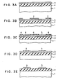
- Example 1 shows a case in which the method according to the present invention is applied to pattern formation on an aluminum film.
- a thick oxide film 2 which has a thickness of about 0.7 ⁇ m is deposited on a silicon substrate 1.
- An Al film (first material film) 3 is formed thereon to a thickness of about 0.8 ⁇ m in order to form an interconnection electrode pattern.
- an SiO 2 film (second material film) 4 is formed by, for example, the plasma CVD method, to a thickness of about 0.5 ⁇ m on the Al film 3.
- the Si0 2 film pattern is formed by general photolithography. Reactive ion etching is performed under the following conditions: the RF power is 0.22 W/cm 2 , the pressure is 10 m Torr, the flow rate of CF 4 is 21 ml/min, and the flow rate of H 2 is 18 ml/min.
- the SiO 2 film 4 is etched at a rate of 400 A/min while a plasma polymer film is deposited at a rate of about 0 100 A/min on the exposed surface of the Al film 3.
- This reactive ion etching is performed for about 8 minutes, and the SiO 2 film 4 is etched and the film thickness is reduced by about 3,000 A, as shown in Fig. 3C.
- a plasma polymer film 5 which has a thickness of about 0 800 A.
- the SiO 2 film 4 is then removed by, for example, fluoric acid as shown in Fig 3D.
- the plasma polymer film 5 is used as a mask and the Al film 3 is etched under proper etching conditions to form a pattern of the Al film 3.
- Etching of the Al film 3 may be performed by the reactive ion etching method, the general dry etching method or the wet etching method using a liquid etchant.
- the 0 2 plasma ashing is performed to remove the plasma polymer film 5. In this manner, the desired interconnection electrode pattern of the Al film 3 is formed, as shown in Fig. 3E.
- the plasma polymer film which is used as the mask for etching the At film has excellent resistance to etching as compared with the mask used in the conventional mask transfer method. Further, stress is not generated between the At film and the mask, and no chemical reaction occurs in the interface therebetween. After the pattern is formed, the plasma polymer film used as the mask is easily eliminated. Furthermore, the plasma polymer film used as the mask provides good step coverage in the level difference of the films, so that irregular pattern formation caused by nonuniform film thickness at the edges of the etching mask where level differences are present is prevented as compared with the conventional pattern forming method, thus providing pattern formation with high reliability.
- Example 1 patterning of the Al film is described.
- the first material film is a low resistant metal film other than aluminum, a polycrystalline silicon film, a single-crystalline silicon film, a silicon nitride film, a copolymer film or the like, the same results are obtained as described in the embodiment above, by using a silicon oxide film as the second material film.
- Examples 2 and 3 show a case in which the method according to the present invention is applied to production of an MOS type semiconductor device.
- a p-type silicon substrate 11 having a crystal orientation of (100) and a specific resistance of 5 to 20 Ocm is used.
- a silicon oxide film 12 is formed 0 thereon to a thickness of about 7,000 A by thermal oxidation as shown in Fig. 4A.
- a polycrystalline siclion film 13 is then deposited on the silicon oxide film 12 to 0 a thickness of about 1,500 A by, for example, the CVD method.
- a resist film 14 is formed on the element formation region by general photolithography.
- the resist film 14 is used as a mask and boron ions are implanted in the field region of the silicon substrate to form layers 15 and 16 as shown in Fig. 4B.
- the acceleration voltage of the boron is preferably at about 350 kV.
- the obtained structure is exposed to a plasma atmosphere containing gas mixture of CF 4 and H 2 in reactive sputtering etching.
- a plasma polymer film 17a of CF x is deposited on the polycrystalline silicon film 13.
- a plasma polymer film 17b is deposited on the resist - film 14.
- the plasma polymer film 17b is removed by removing the resist film 14.
- Fig. 4D shows a case in which the resist film 14 and the plasma polymer film 17b thereon are removed together in a boiling aqueous solution of sulfuric acid and hydrogen peroxide.
- the plasma polymer film 17a formed on the polycrystalline silicon film 13 is partially etched, the plasma polymer film 17a sufficiently acts as a mask for etching the polycrystalline silicon film.
- the polycrystalline silicon film on the element formation region is etched to be removed by using the plasma polymer film 17a as a mask.
- the silicon oxide film 12 of the element formation region is etched by, for example, the reactive sputtering etching method, using the polycrystalline silicon film 13 as an etching mask, as shown in Fig. 4E.
- a gate oxide film 20 is formed, and a gate electrode 21 of a polycrystalline silicon film is deposited over the gate oxide film 20, as shown in Fig. 4F. Further, an n-type impurity such as arsenic is doped to form an n-type source region 22 and an n-type drain region 23 Thereafter, a silicon oxide film 24 is deposited on the entire surface by the CVD method, and contact holes are formed to deposit electrodes 25 and 26.
- the plasma polymer film 17a is deposited on the polycrystalline silicon film 13.
- a film which allows deposition of a plasma polymer film such as an aluminum film, as alumina film or a silicon nitride film, may be used in place of the polycrystalline silicon film 13.
- Example 2 a thick insulating film and a channel stopper are formed in the field region by self-alignment in one photolithography process, in the same manner as in the selective oxidation method. Further, drawbacks of the selective oxidation method described above are eliminated.
- the silicon nitride film which has a resistance to oxidation need not be used, so that degradation of the dielectric strength of the gate oxide film due to the use of the silicon nitride film is eliminated.
- the field insulating film is etched by reactive sputtering etcing, so that the pattern dimentional change becomes substantially zero.
- the area of the element formation region becomes wider than that obtained by the conventional selective oxidation method. Therefore, the packaging density of the elements is greatly increased.
- the packaging density of the elements according to the method of the present invention will be increased by at least 50%.
- the present invention does not require annealing for a long period of time after ion implantation, so that degration of the element characteristics due to relocation of the field stopper is greatly reduced.
- Example 2 the plasma polymer films 17a is formed on the polycrystalline silicon film 13, as shown in Fig. 4C; the plasma polymer film 17b is also formed on the resist film 14. During etching of the resist film 14, the plasma polymer film 17a is made thinner. Further, since boron is implanted by using the resist film 14 as a mask, the film thickness of the resist film 14 must be made great. These problems are eliminated in Example 3.
- a silicon oxide film 32 is deposited on a silicon substrate 31 as in Example 2, and a polycrystalline silicon film 33 is deposited thereover.
- a silicon oxide film 34 which has a thickness of about 7,000 A is formed thereover by the CVD method.
- a resist film 35 is formed on the element formation region by general photolithography.
- the silicon oxide film 34 is patterned by reactive sputtering.
- the resist film 35 and the silicon oxide film 34 are used as masks, and then boron is implanted to form field stoppers 36 and 37.
- the plasma polymer films 38 and 39 are eliminated by oxygen plasma etching and the polycrystalline silicion film 33 is used as the mask to etch the silicon oxide film 32 of the element formation region to form the element isolation region.
- the subsequent steps are the same as in Example 2.
- the elements are deposited on the exposed silicon surface.
- the impurity is not implanted in the element formation region of the silicon substrate.
- the silicon oxide film 34 is etched while the plasma polymer films 38 and 39 are only deposited on the polycrystalline silicon film 33. Therefore, when the silicon oxide film 34 is etched by, for example, a solution of ammonium fluoride, the plasma polymer films 38 and 39 are not substantially etched, so that patterning of the polycrystalline silicon film 33 is performed by the plasma polymer films 38 and 39 with high reliability.
Landscapes
- Drying Of Semiconductors (AREA)
Applications Claiming Priority (4)
| Application Number | Priority Date | Filing Date | Title |
|---|---|---|---|
| JP55150992A JPS5775440A (en) | 1980-10-28 | 1980-10-28 | Manufacture of semiconductor device |
| JP150992/80 | 1980-10-28 | ||
| JP56057899A JPS57172739A (en) | 1981-04-17 | 1981-04-17 | Pattern forming method |
| JP57899/81 | 1981-04-17 |
Publications (2)
| Publication Number | Publication Date |
|---|---|
| EP0050973A1 true EP0050973A1 (de) | 1982-05-05 |
| EP0050973B1 EP0050973B1 (de) | 1986-01-22 |
Family
ID=26398986
Family Applications (1)
| Application Number | Title | Priority Date | Filing Date |
|---|---|---|---|
| EP81305010A Expired EP0050973B1 (de) | 1980-10-28 | 1981-10-23 | Verfahren zur Maskierung von Halbleiteranordnungen unter Verwendung einer Polymerschicht |
Country Status (3)
| Country | Link |
|---|---|
| US (1) | US4371407A (de) |
| EP (1) | EP0050973B1 (de) |
| DE (1) | DE3173581D1 (de) |
Cited By (1)
| Publication number | Priority date | Publication date | Assignee | Title |
|---|---|---|---|---|
| FR2811474A1 (fr) * | 2000-07-07 | 2002-01-11 | Commissariat Energie Atomique | Procede de realisation d'une grille pour une structure de transistor cmos a canal de longueur reduite |
Families Citing this family (12)
| Publication number | Priority date | Publication date | Assignee | Title |
|---|---|---|---|---|
| US4493855A (en) * | 1982-12-23 | 1985-01-15 | International Business Machines Corporation | Use of plasma polymerized organosilicon films in fabrication of lift-off masks |
| US4562091A (en) * | 1982-12-23 | 1985-12-31 | International Business Machines Corporation | Use of plasma polymerized orgaosilicon films in fabrication of lift-off masks |
| US5028555A (en) * | 1987-12-02 | 1991-07-02 | Advanced Micro Devices, Inc. | Self-aligned semiconductor devices |
| US5880036A (en) * | 1992-06-15 | 1999-03-09 | Micron Technology, Inc. | Method for enhancing oxide to nitride selectivity through the use of independent heat control |
| IL112826A (en) * | 1995-02-28 | 1998-09-24 | Chip Express Israel Ltd | Method for depositing a plasma deposited polymer |
| US6255718B1 (en) | 1995-02-28 | 2001-07-03 | Chip Express Corporation | Laser ablateable material |
| US7294578B1 (en) * | 1995-06-02 | 2007-11-13 | Micron Technology, Inc. | Use of a plasma source to form a layer during the formation of a semiconductor device |
| KR100277024B1 (ko) * | 1997-10-31 | 2001-01-15 | 구본준 | 선택적 식각기술을 이용한 액정표시장치 제조방법 |
| ATE433196T1 (de) * | 2001-03-13 | 2009-06-15 | Nat Ct Scient Res Demokritos | Verfahren zur maskierung von silizium für eine anisotrope nassätzung |
| EP1260863A1 (de) * | 2001-05-23 | 2002-11-27 | Scandinavian Micro Biodevices | Mikrostrukturierung von plasma-polymerisierten Beschichtungen |
| US7488687B2 (en) * | 2006-09-12 | 2009-02-10 | Samsung Electronics Co., Ltd. | Methods of forming electrical interconnect structures using polymer residues to increase etching selectivity through dielectric layers |
| CN119890046B (zh) * | 2024-12-26 | 2026-02-24 | 杭州富芯半导体有限公司 | 半导体器件的制备方法及半导体器件 |
Citations (3)
| Publication number | Priority date | Publication date | Assignee | Title |
|---|---|---|---|---|
| US3940506A (en) * | 1973-05-17 | 1976-02-24 | Itt Industries, Inc. | Selective plasma etching and deposition |
| DD138850A1 (de) * | 1978-09-15 | 1979-11-21 | Wolfgang Leyffer | Verfahren zur strukturierung von beschichteten festkoerperoberflaechen durch gasphasenaetzung |
| US4179311A (en) * | 1977-01-17 | 1979-12-18 | Mostek Corporation | Method of stabilizing semiconductor device by converting doped poly-Si to polyoxides |
Family Cites Families (6)
| Publication number | Priority date | Publication date | Assignee | Title |
|---|---|---|---|---|
| NL7607298A (nl) * | 1976-07-02 | 1978-01-04 | Philips Nv | Werkwijze voor het vervaardigen van een inrichting en inrichting vervaardigd volgens de werkwijze. |
| US4140547A (en) * | 1976-09-09 | 1979-02-20 | Tokyo Shibaura Electric Co., Ltd. | Method for manufacturing MOSFET devices by ion-implantation |
| US4244799A (en) * | 1978-09-11 | 1981-01-13 | Bell Telephone Laboratories, Incorporated | Fabrication of integrated circuits utilizing thick high-resolution patterns |
| US4283249A (en) * | 1979-05-02 | 1981-08-11 | International Business Machines Corporation | Reactive ion etching |
| FR2460037A1 (fr) * | 1979-06-22 | 1981-01-16 | Thomson Csf | Procede d'auto-alignement de regions differemment dopees d'une structure de semi-conducteur |
| US4333793A (en) * | 1980-10-20 | 1982-06-08 | Bell Telephone Laboratories, Incorporated | High-selectivity plasma-assisted etching of resist-masked layer |
-
1981
- 1981-10-23 DE DE8181305010T patent/DE3173581D1/de not_active Expired
- 1981-10-23 EP EP81305010A patent/EP0050973B1/de not_active Expired
- 1981-10-28 US US06/315,909 patent/US4371407A/en not_active Expired - Lifetime
Patent Citations (3)
| Publication number | Priority date | Publication date | Assignee | Title |
|---|---|---|---|---|
| US3940506A (en) * | 1973-05-17 | 1976-02-24 | Itt Industries, Inc. | Selective plasma etching and deposition |
| US4179311A (en) * | 1977-01-17 | 1979-12-18 | Mostek Corporation | Method of stabilizing semiconductor device by converting doped poly-Si to polyoxides |
| DD138850A1 (de) * | 1978-09-15 | 1979-11-21 | Wolfgang Leyffer | Verfahren zur strukturierung von beschichteten festkoerperoberflaechen durch gasphasenaetzung |
Non-Patent Citations (1)
| Title |
|---|
| Journal of the Electrochemical Society-Extended Abstracts, Vol. 80, No. 1 May 1980 Princeton ARIKADO et al. "Etching Mechanism of SiO2 in CF4/H2 Mixed Gas Plasma" pages 263 to 265 * |
Cited By (3)
| Publication number | Priority date | Publication date | Assignee | Title |
|---|---|---|---|---|
| FR2811474A1 (fr) * | 2000-07-07 | 2002-01-11 | Commissariat Energie Atomique | Procede de realisation d'une grille pour une structure de transistor cmos a canal de longueur reduite |
| WO2002005336A1 (fr) * | 2000-07-07 | 2002-01-17 | Commissariat A L'energie Atomique | Procede de realisation d'une grille pour une structure de transistor cmos a canal de longueur reduite |
| US6818488B2 (en) | 2000-07-07 | 2004-11-16 | Commissariat A L'energie Atomique | Process for making a gate for a short channel CMOS transistor structure |
Also Published As
| Publication number | Publication date |
|---|---|
| DE3173581D1 (en) | 1986-03-06 |
| US4371407A (en) | 1983-02-01 |
| EP0050973B1 (de) | 1986-01-22 |
Similar Documents
| Publication | Publication Date | Title |
|---|---|---|
| EP0126424B1 (de) | Verfahren zur Herstellung von Polycide-Strukturen | |
| EP0107416B1 (de) | Verfahren zur Herstellung einer Halbleiteranordnung | |
| EP0337299B1 (de) | Verfahren zur Herstellung eines Feld-Effekt-Transistors | |
| US5619064A (en) | III-V semiconductor gate structure and method of manufacture | |
| US6136700A (en) | Method for enhancing the performance of a contact | |
| EP0113517B1 (de) | Verfahren zur Herstellung einer Isolationszone | |
| JPS6231506B2 (de) | ||
| US4371407A (en) | Method for producing semiconductor device | |
| EP0125174A2 (de) | Verfahren zum Herstellen von integrierten Schaltungsstrukturen mit "Replica Patterning" | |
| JPS6072268A (ja) | バイポ−ラ・トランジスタ構造の製造方法 | |
| EP0178000B1 (de) | Verfahren zur Herstellung submikronischer Gräben, z.B. in Halbleitermaterial und nach diesem Verfahren hergestellte Anordnungen | |
| US4398964A (en) | Method of forming ion implants self-aligned with a cut | |
| US4497108A (en) | Method for manufacturing semiconductor device by controlling thickness of insulating film at peripheral portion of element formation region | |
| US4742025A (en) | Method of fabricating a semiconductor device including selective etching of a silicide layer | |
| US5512518A (en) | Method of manufacture of multilayer dielectric on a III-V substrate | |
| EP0095654B1 (de) | Verfahren zum Herstellen einer Halbleiteranordnung mit einem Schritt zum Mustern einer Leiterschicht | |
| JPS6123657B2 (de) | ||
| US5821170A (en) | Method for etching an insulating material | |
| EP0592765A2 (de) | Verfahren zur Herstellung von bipolaren Transistoren mit Heteroübergang | |
| JPS6133253B2 (de) | ||
| US4752815A (en) | Method of fabricating a Schottky barrier field effect transistor | |
| US6191016B1 (en) | Method of patterning a layer for a gate electrode of a MOS transistor | |
| KR100256237B1 (ko) | 콘택홀 형성방법 | |
| EP0037040B1 (de) | Verfahren zur Herstellung einer Halbleitervorrichtung | |
| EP0066675A1 (de) | Verfahren zur Herstellung der Feldeffekttransistoren |
Legal Events
| Date | Code | Title | Description |
|---|---|---|---|
| PUAI | Public reference made under article 153(3) epc to a published international application that has entered the european phase |
Free format text: ORIGINAL CODE: 0009012 |
|
| 17P | Request for examination filed |
Effective date: 19811029 |
|
| AK | Designated contracting states |
Designated state(s): DE FR GB NL |
|
| RAP1 | Party data changed (applicant data changed or rights of an application transferred) |
Owner name: KABUSHIKI KAISHA TOSHIBA |
|
| GRAA | (expected) grant |
Free format text: ORIGINAL CODE: 0009210 |
|
| AK | Designated contracting states |
Designated state(s): DE FR GB NL |
|
| ET | Fr: translation filed | ||
| REF | Corresponds to: |
Ref document number: 3173581 Country of ref document: DE Date of ref document: 19860306 |
|
| PLBE | No opposition filed within time limit |
Free format text: ORIGINAL CODE: 0009261 |
|
| STAA | Information on the status of an ep patent application or granted ep patent |
Free format text: STATUS: NO OPPOSITION FILED WITHIN TIME LIMIT |
|
| 26N | No opposition filed | ||
| PGFP | Annual fee paid to national office [announced via postgrant information from national office to epo] |
Ref country code: FR Payment date: 19961009 Year of fee payment: 16 |
|
| PGFP | Annual fee paid to national office [announced via postgrant information from national office to epo] |
Ref country code: GB Payment date: 19961014 Year of fee payment: 16 |
|
| PGFP | Annual fee paid to national office [announced via postgrant information from national office to epo] |
Ref country code: NL Payment date: 19961029 Year of fee payment: 16 |
|
| PGFP | Annual fee paid to national office [announced via postgrant information from national office to epo] |
Ref country code: DE Payment date: 19961104 Year of fee payment: 16 |
|
| PG25 | Lapsed in a contracting state [announced via postgrant information from national office to epo] |
Ref country code: GB Free format text: LAPSE BECAUSE OF NON-PAYMENT OF DUE FEES Effective date: 19971023 |
|
| PG25 | Lapsed in a contracting state [announced via postgrant information from national office to epo] |
Ref country code: FR Free format text: THE PATENT HAS BEEN ANNULLED BY A DECISION OF A NATIONAL AUTHORITY Effective date: 19971031 |
|
| PG25 | Lapsed in a contracting state [announced via postgrant information from national office to epo] |
Ref country code: NL Free format text: LAPSE BECAUSE OF NON-PAYMENT OF DUE FEES Effective date: 19980501 |
|
| GBPC | Gb: european patent ceased through non-payment of renewal fee |
Effective date: 19971023 |
|
| NLV4 | Nl: lapsed or anulled due to non-payment of the annual fee |
Effective date: 19980501 |
|
| PG25 | Lapsed in a contracting state [announced via postgrant information from national office to epo] |
Ref country code: DE Free format text: LAPSE BECAUSE OF NON-PAYMENT OF DUE FEES Effective date: 19980701 |
|
| REG | Reference to a national code |
Ref country code: FR Ref legal event code: ST |