EP0052226B1 - Digital-Analog-Wandler - Google Patents
Digital-Analog-Wandler Download PDFInfo
- Publication number
- EP0052226B1 EP0052226B1 EP81108090A EP81108090A EP0052226B1 EP 0052226 B1 EP0052226 B1 EP 0052226B1 EP 81108090 A EP81108090 A EP 81108090A EP 81108090 A EP81108090 A EP 81108090A EP 0052226 B1 EP0052226 B1 EP 0052226B1
- Authority
- EP
- European Patent Office
- Prior art keywords
- digital
- analog
- capacitor
- current
- signal
- Prior art date
- Legal status (The legal status is an assumption and is not a legal conclusion. Google has not performed a legal analysis and makes no representation as to the accuracy of the status listed.)
- Expired
Links
- 239000003990 capacitor Substances 0.000 claims description 36
- 238000013459 approach Methods 0.000 description 4
- 238000006243 chemical reaction Methods 0.000 description 3
- 238000005070 sampling Methods 0.000 description 3
- 238000010586 diagram Methods 0.000 description 2
- 230000032683 aging Effects 0.000 description 1
- 230000007423 decrease Effects 0.000 description 1
- 238000000034 method Methods 0.000 description 1
Images

Classifications
-
- H—ELECTRICITY
- H03—ELECTRONIC CIRCUITRY
- H03M—CODING; DECODING; CODE CONVERSION IN GENERAL
- H03M1/00—Analogue/digital conversion; Digital/analogue conversion
- H03M1/06—Continuously compensating for, or preventing, undesired influence of physical parameters
- H03M1/0602—Continuously compensating for, or preventing, undesired influence of physical parameters of deviations from the desired transfer characteristic
- H03M1/0604—Continuously compensating for, or preventing, undesired influence of physical parameters of deviations from the desired transfer characteristic at one point, i.e. by adjusting a single reference value, e.g. bias or gain error
Definitions
- This invention relates to a digital to analog converting apparatus comprising digital to analog converting means having first and second input terminals and generating an analog signal corresponding to a digital signal supplied to the first input terminal and an analog to digital converting means connected to the digital to analog converting means and supplying the second input terminal with a digital signal corresponding to the analog signal generated by the digital to analog converting means, the digital to analog converting means comprising operation means having the first and second input terminals and generating comparison signals representing a difference between two signals supplied to the first and second input terminals, the first input terminal being connected to receive a digital signal, current generating means connected to the operation means for generating current according to the value of the comparison signal, and a capacitor connected to the current generating means, said analog to digital converting means being connected to said capacitor and the second input terminal of said operation means and converting the output voltage of said capacitor to a digital signal.
- D/ A digital to analog
- the switches are opened and closed under the control of the switching control circuit, whereby the resistor ladder circuit divides a power source voltage and generates an analog voltage of a desired value.
- the analog voltage is applied to the comparator through the A/D converter and is then compared with a digital input signal supplied to the comparator.
- the output of the comparator is supplied to the switching control circuit.
- the switching control circuit controls the switches. This sequence of operation is repeated until the two input signals of the comparator come to have the same value.
- the above-mentioned D/A converting apparatus responds very quickly indeed. Provided with a resistor ladder circuit, however, it needs a large circuitry and is inevitably expensive.
- Document US ⁇ A ⁇ 2 855 540 discloses an apparatus comprising a subtractor having first and second input terminals for generating output signals representing a difference between two signals supplied to the first and second input terminal, said first input terminal being connected to an input register and said second input terminal being connected to receive a digital signal which is converted from an analog signal.
- the apparatus further comprises current generating means for generating current according to the value of the aforementioned output signal and a capacitor connected to the output of the current generating means.
- the output of the current generating means and the capacitor are connected to an amplifier the output of which being connected to converter means for supplying a digital signal to said second terminals.
- the subtractor supplies for each pair of digits to be compared as output signal the sign of which controls the direction of current flow through the corresponding current generator, and the value of which is utilized to start and stop the corresponding current generator, whereby each generator supplies a signal having a weight proportional to the numerical weight of the corresponding pair of digits.
- this prior art document does not disclose a D/A converting apparatus but enables a beam positioning system which is independent of voltage variations due to instability and aging of the active components.
- the invention provides a digital to analog converting means as defined above and which is characterized in that said operation means generates two digital comparison signals, in that the current generating means is connected to a power source and has a first current source, a first switching element connected to the first current source, a second switching element connected to the first switching element and a second current source connected to the second switching element, either of the first and second switching elements being rendered conductive according to the value of the corresponding comparison signal, and that the capacitor is connected to the node where the first and second switching elements are connected and can be charged by one of the current sources and discharged by the other current source.
- the invention provides also digital to analog converting means as defined above and which is characterized in that said operation means (14) generates one digital comparison signal, in that said analog to digital converting means (36) is connected to said capacitor (30) via a Darlington pair of transistors, in that the current generating means is connected to a power source and has a current source, a switching element and a diode connected to one end to the node where the current source and switching element are connected, the switching element being rendered conductive according to the value of the comparison signal, and that the capacitor is connected to the other end of said diode and charged by the current source, and discharged by said Darlington pair of transistors.
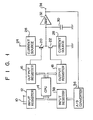
- Fig. 1 shows a first embodiment of this invention.
- An input terminal 10 is connected to an input register 12.
- An output signal of the input register 12 is supplied to a central processing unit 14 (hereinafter called "CPU 14").
- CPU 14 central processing unit 14
- An output signal of the CPU 14 is coupled to two output registers 16 and 18.
- An output signal of the output register 16 is coupled to a gate of an N channel MOS FET 20, and an output signal of the output register 18 to a gate of an N channel MOS FET 22.
- Both MOS FETs 20 and 22 function as an analog switch.
- a power source terminal 24 of positive polarity is grounded via a current source 26, MOS FETs 20 and 22 and another current source 28.
- the current sources 26 and 28 are each constituted by, for example, a resistor.
- the current source 26 supplies current to the MOS FET 20, and the current source 28 receives current from the MOS FET 22.
- the node where the MOS FETs 20 and 22 are connected is grounded via a capacitor 30 and is connected to a voltage follower amplifier 32 of a high input impedance.
- the output terminal of the amplifier 32 is connected to an output terminal 34 and also to an A/D converter 36.
- An output signal of the A/D converter 36 is supplied to an input register 38, an output signal of which is supplied to the CPU 14.
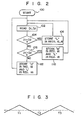
- FIG. 2 of a flow chart, it will be described how the above-mentioned embodiment of Fig. 1 operates.
- the AID converter 36 supplies the input register 38 with a digital voltage D2 which corresponds to the output of the amplifier 32, i.e. the output voltage of the capacitor 30 amplified.
- a step 100 the CPU 14 is started.
- a step 102 it reads the data D1 and D2 from the input registers 12 and 38, respectively.
- a step 104 it determines if D1 and D2 are equal. If D1 and D2, i.e. the digital input value and analog output value, are found equal, the CPU 14 proceeds to a step 106, wherein an L signal is stored into both the output registers 16 and 18. If D1 and D2 are not found equal, the CPU 14 further judges in a step 108 whether D1 is greater than D2 or not. As long as the L signal is stored in both the output registers 16 and 18, the MOS FETs 20 and 22 remain non-conductive and the output voltage of capacitor 30 remains unchanged.
- step 110 If D1 is found greater than D2 in the step 108, that is, if the digital input value supplied to the input register 12 is greater than the analog output value supplied to the output terminal 34, the CPU 14 proceeds to a step 110.
- an H signal is stored into the output register 16, and an L signal into the output register 18.
- the MOS FET 20 becomes conductive, and the MOS FET 22 becomes non-conductive.
- an output current flows from the current source 26 via the MOS FET 20 and the capacitor 30 is therefore charged.
- the output voltage of the capacitor 30 then rises and is supplied to the A/D converter 36. Consequently, D2 grows, and the analog output value approaches the digital input value.
- H and L signals are stored in a step 112 respectively into the output registers 18 and 16.
- the MOS FET 20 becomes non-conductive, and the MOS FET 22 becomes conductive.
- the capacitor 30 is discharged and current flows via the MOS FET 22 to the current source 28. Consequently, the output voltage of the capacitor 30 lowers and D2 becomes smaller and thus approaches D1.
- the CPU 14 proceeds again to the step 102 and reads data D1 and D2 from the input registers 12 and 38, respectively. Thereafter, the steps 104, 106, 108, 110 and 112 are repeated once or more times until the analog value supplied to the output terminal 34 becomes equal to the digital input value supplied to the input terminal 10.
- the A/D converter 36 converts the analog output value to a digital value during every sampling period.
- the output voltage of the A/D converter 36 may therefore fluctuate from the true value as illustrated in Fig. 3, wherein the broken line is the true value and T1, T2 and T3 are sampling time. This does not matter at all.
- the fluctuation would be 10 mA at most when both the current sources 26 and 28 supply 0.1 mA, the capacitor 30 has a capacitance of 50 J,lF and the sampling cycle is 5 ms.
- the apparatus of Fig. 1 uses a capacitor instead of a resistor ladder circuit. It is therefore a digital to analog converting apparatus which is small, simple and inexpensive.
- the CPU 14 may be used not only to achieve analog to digital conversion but also to perform other operations. If the CPU 14 is used in this way, interruption will be effected upon completion of the analog to digital conversion, thereby the operations shown in Fig. 2 are carried out. Once the CPU 14 has stored signals into the output registers 16 and 18, it remains waiting for next interruption. Other devices than the CPU 14 may be used to compare the digital input with the analog output. For example, a discrete comparator or a logic circuit may be used for the purpose. Further, the CPU 14, A/D converter 36 and registers 12 and 38 may be replaced by a microcomputer. Still further, instead of the MOS FETs, bipolar transistors, relay switches, etc. may be used for the analog switches.
- Fig. 4 shows a second embodiment of this invention.
- same numerals are used to denote the same elements as shown in Fig. 1.
- This embodiment is identical with the embodiment of Fig. 1, except that it is not provided with the output register 16 and analog switch 20.
- an output terminal of an output register 18 is connected to a base of an NPN transistor 22.
- the transistor 22 functions as an analog switch, and its emitter is grounded and its collector is connected to an anode of a diode 40.
- a power source terminal 24 is connected to an input terminal of a current source 42.
- the current source 42 supplies current to the transistor 22.
- a cathode of the diode 40 is grounded via a capacitor 30 and connected to an output terminal 34 via a Darlington pair of transistors 44.
- the output terminal of the Darlington pair of transistors 44 is connected also to an A/D converter 36.
- Fig. 5 of a flow chart it will be described how the embodiment of Fig. 4 operates when the input registers 12 and 38 receive data D1 and D2, respectively.
- a step 202 the CPU 14 reads D1 and D2 respectively from the input registers 12 and 38.
- a step 204 it is judged if D1 is greater than D2. If D1 is found greater than D2, that is, if the digital input value is greater than the analog output value, the CPU 14 proceeds to a step 206, wherein an L signal is stored into the output register 18. In this case, the transistor 22 is non-conductive. As a result, the output current of the current source 42 flows into the capacitor 30 via the diode 40, thus raising the output voltage of the capacitor 30. Consequently, the analog output value approaches the digital input value.
- the steps 202, 204 and 206 are repeated in sequence, once or more times, until the analog output value increases to be equal to the digital input value.
- the steps 202, 204 and 208 are repeated in sequence, once or more times, until the analog output value decreases to be equal to the digital input value.
- an analog voltage corresponding to the digital input value will at last be obtained at the output terminal 34.
- Fig. 4 uses a Darlington pair of transistors in place of such a current source as used in the embodiment of Fig. 1 to discharge the capacitor 30.
- a leak current of the Darlington pair of transistors is used to discharge the capacitor 30. This technique renders the apparatus of Fig. 4 simpler than that of Fig. 1.
Landscapes
- Engineering & Computer Science (AREA)
- Theoretical Computer Science (AREA)
- Analogue/Digital Conversion (AREA)
Claims (4)
Applications Claiming Priority (2)
| Application Number | Priority Date | Filing Date | Title |
|---|---|---|---|
| JP55159929A JPS5783926A (en) | 1980-11-13 | 1980-11-13 | Digital to analog converter |
| JP159929/80 | 1980-11-13 |
Publications (2)
| Publication Number | Publication Date |
|---|---|
| EP0052226A1 EP0052226A1 (de) | 1982-05-26 |
| EP0052226B1 true EP0052226B1 (de) | 1986-04-16 |
Family
ID=15704230
Family Applications (1)
| Application Number | Title | Priority Date | Filing Date |
|---|---|---|---|
| EP81108090A Expired EP0052226B1 (de) | 1980-11-13 | 1981-10-08 | Digital-Analog-Wandler |
Country Status (4)
| Country | Link |
|---|---|
| US (1) | US4547762A (de) |
| EP (1) | EP0052226B1 (de) |
| JP (1) | JPS5783926A (de) |
| DE (1) | DE3174411D1 (de) |
Families Citing this family (8)
| Publication number | Priority date | Publication date | Assignee | Title |
|---|---|---|---|---|
| US5610810A (en) * | 1981-09-06 | 1997-03-11 | Canon Kabushiki Kaisha | Apparatus for correcting errors in a digital-to-analog converter |
| JPS61169024A (ja) * | 1985-01-21 | 1986-07-30 | Fujitsu Ltd | アナログ出力処理方式 |
| US4633164A (en) * | 1985-12-20 | 1986-12-30 | Beckman Industrial Corporation | Microprocessor controlled constant current circuit |
| US5021730A (en) * | 1988-05-24 | 1991-06-04 | Dallas Semiconductor Corporation | Voltage to current converter with extended dynamic range |
| US4866301A (en) * | 1988-05-24 | 1989-09-12 | Dallas Semiconductor Corporation | Controlled slew peak detector |
| GB8813162D0 (en) * | 1988-06-03 | 1988-07-06 | British Telecomm | Digital-to-analogue conversion |
| US5638072A (en) * | 1994-12-07 | 1997-06-10 | Sipex Corporation | Multiple channel analog to digital converter |
| EP1490974A4 (de) * | 2001-11-30 | 2006-02-22 | Second Sight Medical Prod Inc | Floating-gate-digital/analog-umsetzer |
Family Cites Families (10)
| Publication number | Priority date | Publication date | Assignee | Title |
|---|---|---|---|---|
| US3258765A (en) * | 1966-06-28 | Vfe%time | ||
| DE1069683B (de) * | 1956-04-27 | 1959-11-26 | Western Electric Company, Incorporated, New York, N. Y. (V. St. A.) | System zur Elektronenstrahleinstellung durch Codesignale |
| US3252045A (en) * | 1961-01-16 | 1966-05-17 | Marquardt Corp | Line generating means and method |
| FR1359346A (fr) * | 1963-03-15 | 1964-04-24 | Etude Et La Realisation Des Pr | Asservissement de position de haute précision |
| US3518658A (en) * | 1964-12-16 | 1970-06-30 | Ibm | Digital comparison-to-analog signal converter |
| US3523229A (en) * | 1967-01-05 | 1970-08-04 | Ibm | Digital-analog servo system |
| US4023122A (en) * | 1975-01-28 | 1977-05-10 | Nippon Electric Company, Ltd. | Signal generating circuit |
| FR2396463A1 (fr) * | 1977-06-30 | 1979-01-26 | Ibm France | Circuit pour compenser les decalages du zero dans les dispositifs analogiques et application de ce circuit a un convertisseur analogique-numerique |
| JPS5534618A (en) * | 1978-08-29 | 1980-03-11 | Mamoru Kato | Annealing apparatus |
| US4225825A (en) * | 1978-09-25 | 1980-09-30 | Beckman Instruments, Inc. | Precision self-adjusting slope circuit |
-
1980
- 1980-11-13 JP JP55159929A patent/JPS5783926A/ja active Pending
-
1981
- 1981-10-08 DE DE8181108090T patent/DE3174411D1/de not_active Expired
- 1981-10-08 EP EP81108090A patent/EP0052226B1/de not_active Expired
-
1984
- 1984-02-13 US US06/578,607 patent/US4547762A/en not_active Expired - Lifetime
Also Published As
| Publication number | Publication date |
|---|---|
| US4547762A (en) | 1985-10-15 |
| DE3174411D1 (en) | 1986-05-22 |
| JPS5783926A (en) | 1982-05-26 |
| EP0052226A1 (de) | 1982-05-26 |
Similar Documents
| Publication | Publication Date | Title |
|---|---|---|
| EP0115897B1 (de) | Stromquellenanordnung | |
| US5289191A (en) | Bipolar analog-to-digital conversion apparatus with unipolar current and voltage modes | |
| EP0419093A2 (de) | Strommessschaltung | |
| EP0580923A1 (de) | Schaltung zum Messen der auf reinen Spannungssollwert bezogenen Spannungsschwankungen für Fehlerverstärker enthaltende Vorrichtungen | |
| US4766328A (en) | Programmable pulse generator | |
| JPH02215222A (ja) | ハーフブリッジ様式に接続されたトランジスタのためのドライブ信号発生器 | |
| US20040135567A1 (en) | Switching regulator and slope correcting circuit | |
| KR100722065B1 (ko) | 전원장치 | |
| EP0052226A1 (de) | Digital-Analog-Wandler | |
| US5124630A (en) | Switching power supply apparatus | |
| KR920004347B1 (ko) | 아나로그/디지탈변환회로 | |
| GB2236444A (en) | Current mirror | |
| FI65518C (fi) | Digitalreglersystem | |
| KR100270033B1 (ko) | 충전 장치, 전류 검출 회로 및 전압 검출 회로 | |
| US4415815A (en) | Electronic switch | |
| US4525636A (en) | Variable electronic impedance circuit | |
| US4339669A (en) | Current ramping controller circuit | |
| US4358689A (en) | Analog to digital interface circuit | |
| US6069577A (en) | A/D conversion device provided with a gain calibration arrangement | |
| EP0196131A1 (de) | Verstärkeranordnung | |
| US5994928A (en) | Rapidly charged sample-and hold circuit | |
| US5144310A (en) | A/D converter utilizing successive approximation | |
| EP0372547B1 (de) | Vorspannungsschaltung für einen nach dem Prinzip der Unterteilung arbeitenden Analog-Digitalwandler | |
| US4085340A (en) | Range switching transient eliminator circuit | |
| US3227895A (en) | Signal differential comparator amplifier |
Legal Events
| Date | Code | Title | Description |
|---|---|---|---|
| PUAI | Public reference made under article 153(3) epc to a published international application that has entered the european phase |
Free format text: ORIGINAL CODE: 0009012 |
|
| 17P | Request for examination filed |
Effective date: 19811019 |
|
| AK | Designated contracting states |
Designated state(s): DE FR GB |
|
| RAP1 | Party data changed (applicant data changed or rights of an application transferred) |
Owner name: KABUSHIKI KAISHA TOSHIBA |
|
| GRAA | (expected) grant |
Free format text: ORIGINAL CODE: 0009210 |
|
| AK | Designated contracting states |
Kind code of ref document: B1 Designated state(s): DE FR GB |
|
| REF | Corresponds to: |
Ref document number: 3174411 Country of ref document: DE Date of ref document: 19860522 |
|
| ET | Fr: translation filed | ||
| PLBE | No opposition filed within time limit |
Free format text: ORIGINAL CODE: 0009261 |
|
| STAA | Information on the status of an ep patent application or granted ep patent |
Free format text: STATUS: NO OPPOSITION FILED WITHIN TIME LIMIT |
|
| 26N | No opposition filed | ||
| PGFP | Annual fee paid to national office [announced via postgrant information from national office to epo] |
Ref country code: GB Payment date: 19960930 Year of fee payment: 16 |
|
| PGFP | Annual fee paid to national office [announced via postgrant information from national office to epo] |
Ref country code: FR Payment date: 19961009 Year of fee payment: 16 |
|
| PGFP | Annual fee paid to national office [announced via postgrant information from national office to epo] |
Ref country code: DE Payment date: 19961011 Year of fee payment: 16 |
|
| PG25 | Lapsed in a contracting state [announced via postgrant information from national office to epo] |
Ref country code: GB Free format text: LAPSE BECAUSE OF NON-PAYMENT OF DUE FEES Effective date: 19971008 |
|
| PG25 | Lapsed in a contracting state [announced via postgrant information from national office to epo] |
Ref country code: FR Free format text: THE PATENT HAS BEEN ANNULLED BY A DECISION OF A NATIONAL AUTHORITY Effective date: 19971031 |
|
| GBPC | Gb: european patent ceased through non-payment of renewal fee |
Effective date: 19971008 |
|
| PG25 | Lapsed in a contracting state [announced via postgrant information from national office to epo] |
Ref country code: DE Free format text: LAPSE BECAUSE OF NON-PAYMENT OF DUE FEES Effective date: 19980701 |
|
| REG | Reference to a national code |
Ref country code: FR Ref legal event code: ST |