EP0052950A1 - Optischer Randdetektor - Google Patents
Optischer Randdetektor Download PDFInfo
- Publication number
- EP0052950A1 EP0052950A1 EP81305107A EP81305107A EP0052950A1 EP 0052950 A1 EP0052950 A1 EP 0052950A1 EP 81305107 A EP81305107 A EP 81305107A EP 81305107 A EP81305107 A EP 81305107A EP 0052950 A1 EP0052950 A1 EP 0052950A1
- Authority
- EP
- European Patent Office
- Prior art keywords
- light
- phototransistor
- channel
- edge detector
- collimating
- Prior art date
- Legal status (The legal status is an assumption and is not a legal conclusion. Google has not performed a legal analysis and makes no representation as to the accuracy of the status listed.)
- Withdrawn
Links
Images

Classifications
-
- G—PHYSICS
- G06—COMPUTING OR CALCULATING; COUNTING
- G06M—COUNTING MECHANISMS; COUNTING OF OBJECTS NOT OTHERWISE PROVIDED FOR
- G06M1/00—Design features of general application
- G06M1/08—Design features of general application for actuating the drive
- G06M1/10—Design features of general application for actuating the drive by electric or magnetic means
- G06M1/101—Design features of general application for actuating the drive by electric or magnetic means by electro-optical means
-
- G—PHYSICS
- G01—MEASURING; TESTING
- G01S—RADIO DIRECTION-FINDING; RADIO NAVIGATION; DETERMINING DISTANCE OR VELOCITY BY USE OF RADIO WAVES; LOCATING OR PRESENCE-DETECTING BY USE OF THE REFLECTION OR RERADIATION OF RADIO WAVES; ANALOGOUS ARRANGEMENTS USING OTHER WAVES
- G01S17/00—Systems using the reflection or reradiation of electromagnetic waves other than radio waves, e.g. lidar systems
- G01S17/02—Systems using the reflection of electromagnetic waves other than radio waves
- G01S17/04—Systems determining the presence of a target
-
- G—PHYSICS
- G01—MEASURING; TESTING
- G01S—RADIO DIRECTION-FINDING; RADIO NAVIGATION; DETERMINING DISTANCE OR VELOCITY BY USE OF RADIO WAVES; LOCATING OR PRESENCE-DETECTING BY USE OF THE REFLECTION OR RERADIATION OF RADIO WAVES; ANALOGOUS ARRANGEMENTS USING OTHER WAVES
- G01S7/00—Details of systems according to groups G01S13/00, G01S15/00, G01S17/00
- G01S7/48—Details of systems according to groups G01S13/00, G01S15/00, G01S17/00 of systems according to group G01S17/00
- G01S7/481—Constructional features, e.g. arrangements of optical elements
- G01S7/4811—Constructional features, e.g. arrangements of optical elements common to transmitter and receiver
- G01S7/4813—Housing arrangements
Definitions
- the present invention relates in general to optical sensors, and in particular to leading edge detectors used to measure the time it takes a linearly moving, light-reflective surface to travel from one point to another.
- the invention finds particular application in the calibration of moving belt conveyors used to accurately meter quantities of bulk material carried by the conveyor, such as coal being fed to a power plant boiler.
- Modern conveyors of this type normally include a belt speed transducer providing an electronic signal indicative of belt travel or velocity. This signal is used with other conveyor parameters to indicate and regulate the amount (weight, volume, etc.) of material being delivered by the moving belt as a function of time.
- One method of measuring actual belt speed requires the use of a pair of leading edge detectors precisely spaced apart from each other and positioned in like orientation along one edge of the moving belt.
- a piece of light-reflective tape is affixed to the moving belt edge adjacent the detectors.
- a signal such as a fast rise-time pulse, is generated by the detector to indicate such a passage.
- An optical edge detector for use in such a belt speed measuring method is desirably of rugged and simple construction so as to tolerate the hostile environment wherein a majority of bulk material metering conveyors, such as power plant coal feeding conveyors, are located. Further, the detectors as a pair used as noted above must be designed to provide high accuracy under conditions where the belt edge carrying the reflective tape wanders from side to side along its generally linear path of movement. As the tape passes one edge detector, the distance between that edge detector and the tape will more than likely differ from the distance between the tape and the next edge detector due to side-to-side wandering of the belt. Such belt wandering must be considered in designing an edge detector for use as noted above.
- an optical edge detector comprising: an incoherent light source for illuminating at a predetermined wavelength range an area through which a relatively moving light-reflective surface passes, a photosensitive semiconductor element responsive primarily to said predetermined wavelength range, an incoherent, light-collimating, lensless channel positioned for light communication between at least one of said source and element and said illuminated area, the length of the channel being substantially greater than its width, and a pulse generating circuit having an input connected to the photosensitive semiconductor element and an output for providing a fast rise-time pulse generally at the time of entry of the leading edge of the light-reflective surface into the field of view of the photosensitive semiconductor within said illuminated area, said fast rise-time pulse being generated upon a rapid change in the conductivity state of said photosensitive semiconductor element in response to reflected light from said leading edge, said reflected light being provided by the light source to the photosensitive semiconductor element via said collimating channel.
- the detector includes a pair of generally identical plates precisely spaced apart from each other in parallel relation to define the width of the collimating channel.
- the light source comprises a pair of pulse powered, infrared, light-emitting diodes mounted at one end of the plate pair and the photosensitive element comprises an infrared sensitive phototransistor positioned between the diodes and equidistantly spaced from them.
- the diodes illuminate an area adjacent the other end of the plate pair within the field of view of the phototransistor. A light-reflective surface passing across such area is detected by reflecting infrared light provided by the diodes back to the phototransistor via the collimating channel.
- the detector in another emebodiment, includes a straight tubular element in place of the plate pair noted above.
- the tubular element is closed at one end by a cap having a rectangular aperture defining the width of the collimating channel, the diodes and phototransistor being located at the other end of the tubular element.
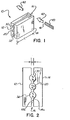
- an optical sensor 10 including a first collimator channel defining plate 12 and a second collimator channel defining plate 14, the plates being generally identical to each other and spaced apart in parallel relation to define a light-collimating, lensless channel 16.
- the plates 12,14 can be formed of any suitable material, such as metal, plastic, or the like.
- the width W of the collimating channel 16 is substantially less than the length L of the plates 12,14. For example, the width W is in the range of .025 to .100 inch, while the length L is in the range of 4.0 to 4.5 inches.
- the plates 12, 14 are held in position relative to each other, as illustrated in FIGS. 1 and 2, by conventional means (not illustrated).
- a phototransistor 20 Mounted at the rearward end of the sensor 10, i.e., the leftward end as viewed in FIG. 1, is an array of semiconductor elements including a photosensitive semiconductor in the preferred form of a phototransistor 20 which is center- counted between the plates 12, 14 at the rear end of the collimating channel 16 by any suitable means. Bracketing the phototransistor 20 are a pair of light-emitting diodes, including a first light-emitting diode 30 and a second light-emitting diode 32.
- the diodes 30,32 are each equidistantly spaced from the phototransistor 20 and together comprise an incoherent light source for illuminating a light-reflective surface 40 having a leading edge 41 passing into and through the field of view of the phototransistor 20 along a linear path indicated by arrows 42, such linear path being generally perpendicular to and traversing the collimating channel 16.
- the phototransistor 20 and the light-emitting diodes 30, 32 are centered between the inner walls 12a, 14a of the plates 12 and 14, with the cases of the transistor 20 and the diodes 30,32 being preferably embedded in appropriately sized recesses in the plates so that a width W in the range of .025 to .100 inch can be provided.
- the inner walls 12a,14a are preferably of a flat black finish to minimize spurious light reflections.
- a longitudinal view axis 20a and longitudinal illumination axes 30a, 32a of the phototransistor 20 and the diodes 30, 32, respectively, are parallel to the walls 12a, 14a and centered in the collimating channel 16, as will be seen more clearly with reference to FIGS. 3 and 4.
- FIGS. 3 and 4 there is illustrated in greater detail the preferred geometric orientation of the phototransistor 20 and the light-emitting diodes 30, 32 relative to each other and to the plates 12,14 defining lensless collimating channel 16 (FIG. 1).
- the phototransistor 20 is of conventional design, and includes an optical lens 21 having the longitudinal view axis 20a and a field of view defined by lines Ql,Q'l and Q2,Q'2.
- the diodes 30,32 are likewise of conventional design and include longitudinal view axes 30a, 32a.
- the field of view or the field of illumination of the first diode 30 is defined by a pair of axis lines Dl and D'l, while the field of illumination of the second diode 32 is defined by axis lines D2 and D'2.
- Electrical connection for the transistor 20 to an external circuit means is provided by a collector lead 22, a base lead 23, and an emitter lead 24, while the light-emitting diodes 30,32 include respective anode leads 34,36 and cathode leads 35,37.
- the diodes 30,32 include conventional optical lenses 31,33 through which light is provided to illuminate their respective fields of view, the axes 30a,32a being generally parallel on the axis 20a of the phototransistor 20.
- the overlapping fields of view of the phototransistor 20 and the diode pair 30,32 serve to define an illuminated edge detection zone or sector d, as illustrated in FIGS. 3 and 4, through which the light-reflective surface 40 having a leading edge 41 will pass and be detected in a manner to be described.
- the present invention finds particular use wherein a pair of the sensors 10 are precisely positioned a known distance from each other along the edge of a moving belt to which a piece of reflective tape is fas- tened, the tape constituting the reflective surface 40 having the leading edge 41.
- the edge of the belt, and thus the leading edge 41 may wander to a limited degree from side to side of its generally linear movement path, as illustrated by arrows 42 (FIG. 1), as it moves between the two sensors.
- the leading edge 41 Upon entering the detection sector d, the leading edge 41 will reflect light from the light-emitting diodes 30,32 back to the phototransistor 20 to trigger a pulse-generating circuit (to be subsequently illustrated), thus indicating the detection of the light-reflective surface 40.
- the light-reflective surface 40 may be at a position (such as position 43) close to the first sensor only to move or wander away from the second detector (such as to position 44), wherein errors in the measuring of time and travel of the leading edge 41 from one sensor to the other could result, since the upstream edge (axis Q'2) of the phototransistor's field of view is not always perpendicular to the path of linear movement followed by the reflective surface 40.
- the spread angle ⁇ (see FIG. 4) of the detection sector is limited to about .5 0 or less by minimizing the width of the collimator channel 16 and maximizing the collimator channel length 1 to the degree feasible.
- the width W is chosen to be .075 inch, while the collimator channel length 1 is 4.3 inches.
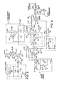
- FIGS. 5 and 6 there is illustrated a . suitable light-emitting diode power circuit (FIG. 5) and a pulse generating circuit (FIG. 6) for use with the optical edge detecting sensor 10 discussed earlier.
- FIGS. 5 and 6 there is illustrated a . suitable light-emitting diode power circuit (FIG. 5) and a pulse generating circuit (FIG. 6) for use with the optical edge detecting sensor 10 discussed earlier.
- the circuit of FIG. 5 simultaneously pulses, at relatively high current levels, the light-emitting diodes 30 and 32.
- a high frequency, low duty cycle, square wave oscillator is necessary to trigger the diodes 30,32 into and out of conduction.
- the oscillator includes a conventional CMOS-type Schmitt trigger 55 inverter with hysteresis, having connected across it a high-time resistor 56 and a low-time resistor and charging diode network 58.
- a frequency determining capacitor 57 cooperates in alternating fashion with the resistor 56 or the network 58 to trigger the inverter 55 output between digital states, preferably at about a 20 KHz rate, although a frequency range of 10-30 KHz is acceptable.
- the duty cycle of the square pulses provided at the output of the inverter 55 can be varied to establish a desired duty cycle.
- a duty cycle of about 10 to 30 percent has been found to be acceptable in practicing the teaching of the present invention.
- the output of the inverter 55 is provided, via a second Schmitt trigger inverter 59, with hysteresis, to the gate electrode 51 of a high power metal oxide semiconductor field effect transistor (MOSFET).
- MOSFET metal oxide semiconductor field effect transistor
- the transistor 50 is capable of handling high current and controlling it with very low gate voltages of very short duration, e.g., in the 2-4 volt and 100-200 nano second range.
- the light-emitting diodes 30,32 are connected in series with each other, with their cathode ends connected to the drain electrode 52 of the transistor 50.
- the anode end of the light-emitting diode pairs 30,32 is connected to electrical ground via a conventional current limiting resistor 54, while the source electrode 53 of the transistor 50 is tied to the negative side of the supply voltage.
- the diodes 30,32 are pulsed on and off at a 20 KHz rate and at a relatively low duty cycle of 20 to 30 percent, wherein high current on the order of 1 amp can flow through them to effect bursts of high illumination light output, preferably primarily in the infrared wavelength range. It has been found that the use of infrared type diodes (and an infrared-sensitive phototransistor) minimizes problems caused by ambient light and enhances the detection capabilities of the sensor in accordance with the present invention.
- FIG. 6 there is illustrated a suitable fast rise-time pulse generating circuit connected to the phototransistor 20 illustrated and discussed earlier with regard to FIGS. 1 through 4.
- the phototransistor 20 is included as part of a photosensitive network wherein the emitter electrode 24 of the phototransistor 20 is tied to the negative side of the supply via a DC current providing resistor 62, which is paralleled by a bypass capacitor 61 which yields a high gain to a rapid change in the conductivity state of the phototransistor 20.
- a base-emitter junction biasing resistor 60 is connected between the base electrode 23 and emitter electrode 24 to bias the base-emitter junction of the phototransistor 20 in a conventional manner.
- the collector electrode 22 is connected to the inverting input of an operational amplifier 70 (connected in a differential amplifier configuration) having its output connected back to its inverting input via a feedback resistor 72.
- a reference voltage is established at the non-inverting input of the op amp 70 in a manner to be subsequently discussed.
- the output of the amplifier 70 is connected both to a first filter network Fl and a second filter network F2.
- the filter network Fl includes an input diode 90, an input resistor 92, and an RC network comprised of a resistor 96 and a capacitor 94.
- the second filter network F2 includes an input diode 80, an input resistor 82, and an RC circuit comprised of a pair of resistors 86 and 88 and a capacitor 84.
- the filter networks Fl, F2 comprise demodulation filters having different response times.
- the networks are both passive and of conventional construction.
- the output 99 of the first filter is fed to the non-inverting input 114 of a comparator-connected operational amplifier 118 via an operational amplifier buffer 100 connected in a voltage follower configuration.
- the output 89 of the second filter in turn is fed to the inverting input 116 of the comparator 118.
- a feedback resistor 112 is connected between the output of the comparator 118 and its non-inverting input 114, while an input resistor 110 is placed in series between the output of the buffer op amp 100 and the non-inverting input 114.
- the output of the comparator 118 is connected to a level translator, including a resistor 120 and diode 122, the level translator serving in a conventional fashion to modify one digital input signal at a pair of voltage levels to a second digital input signal at a different pair of voltage levels.
- the output of the level translator in turn is fed to a pair of paralleled Schmitt trigger inverters 124 with hysteresis to provide at their combined outputs a fast rise-tine pulse.
- a stabilization network is provided between the buffer 100 and the non-inverting input of the op amp 70.
- Inputs to the stabilization circuit include a capacitor 133 having one end connected to the output 99 of the first filter Fl and the - output of a stabilization op amp 130.
- the input to the stabilization network also includes an input line 102 connected from the output of the buffer amp 100 to the inverting input of the stabilization op amp 130 via a resistor 134.
- An integrator functioning feedback capacitor 132 is connected in conventional fashion across the output and inverting input of the op amp 130 having a reference voltage established at its non-inverting input by a voltage divider network comprised of a pair of resistors 135.
- the output of the stabilization amp 130 is connected to establish a floating reference voltage at the non-inverting input of the op amp 70 via a resistor 136.
- the stabilization network serves as an automatic gain control to vary the reference voltage at the noninverting input of the op amp 70 in accordance with temperature variations and ambient light conditions experienced at the base-emitter junction of the phototransistor 20.
- the operation of the circuit illustrated in FIG. 6 and its design are conventional in nature, and it operates in a general manner as follows.
- Ambient light variations and temperature variations at the base-emitter junction of the phototransistor 20 may cause small variations in the conductivity state of the phototransistor 20, such small variances being compensated for via the stabilization network to preclude any spurious pulse output from the Schmitt trigger network 124.
- the pulsating, high frequency, short duration light output bursts from the infrared diodes 30 and 32 are reflected from the leading edge back to the phototransistor 20 via the collimator channel 16.
- the phototransistor 22 is of a type that is primarily sensitive to the infrared light range generated by the diodes 30, 32. Such reflective light causes a rapid, quantitative switch in the conductivity level of the phototransistor 20.
- the transistor 20 is forced into or near saturation, wherein the voltage state at the inverting input of the amplifier 70 changes relative to the current reference voltage at the non-inverting input of the amplifier 70.
- An output signal is generated by the op amp 70, such output signal being provided simultaneously to the filters Fl and F2.
- the comparator 118 having its input tied to the outputs of the two filters, will, in response to the conductivity change of the phototransistor 20, provide an output signal that is then shaped into a fast rise-time digital pulse via the level translator and the Schmitt trigger network 124.
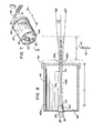
- FIGS. 7 and 8 illustrate another embodiment of the invention for use with the circuitry of FIGS. 5 and 6, wherein a straight tubular element 140functions in a manner generally identical to the plates 12, 14 illustrated earlier to provide the light collimating channel 16.
- An end cap 142 closes one end of the tubular element and includes a rectangular aperture or slot defined by slot walls 142a, 142b defining the width W and height of the collimating channel.
- the interior surface 140a of the tubular element 140 is preferably of a flat black finish to minimize spurious light reflections.
- the tubular element 140 and the end cap 142 can be formed of metal, plastic or the like.
- the phototransistor 20 bracketed by the diodes 30, 32 Located and fixed at the other end of the tubular element 140 by a suitable support structure 144 such as a circuit board type mounting plate is the phototransistor 20 bracketed by the diodes 30, 32.
- the elements 20, 30 and 32 lie in the plane generally defined by the rectangular aperture or slit provided by the end cap 142.
- the width W of the end cap aperture defines the width of the rectangular colli- mating channel 16 (indicated by the axis lines 16a, 16b) while the length 1 of the tubular element 142 is approximately equal to the collimator channel length.
- the length and width dimensions (1 and W) are preferably in the range discussed earlier with regard to the embodiment of FIGS 1 through 4 to limit the spread angle 6 for the reasons noted above.
- the present invention as illustrated by the embodiment in FIGS. 1 through 4, and in FIGS. 7 and 8, when combined with the circuitry of FIGS. 5 and 6, provides a very rugged sensor for detecting the incidence of the leading edge of a light-reflective surface into its field of view. Further, the use of a pair of sensors and their accompanying circuitry to calibrate conveyor belt speed, as discussed above, has proved to be highly accurate.
- the sensor in accordance with the invention is very low in cost as compared with other systems, such as those based on lasers. Finally, the sensor in accordance with the invention is safe for handling by service personnel, since only relatively low voltages . ( ⁇ 15 volts) are typically present, as opposed to a laser- based system wherein dangerously high voltages in the kilovolt region are typically present along with laser light that can be harmful even at low power levels to the eye retina, for example.
Landscapes
- Physics & Mathematics (AREA)
- Engineering & Computer Science (AREA)
- General Physics & Mathematics (AREA)
- Electromagnetism (AREA)
- Computer Networks & Wireless Communication (AREA)
- Radar, Positioning & Navigation (AREA)
- Remote Sensing (AREA)
- Theoretical Computer Science (AREA)
- Length Measuring Devices By Optical Means (AREA)
- Photometry And Measurement Of Optical Pulse Characteristics (AREA)
- Optical Transform (AREA)
Applications Claiming Priority (4)
| Application Number | Priority Date | Filing Date | Title |
|---|---|---|---|
| US21072280A | 1980-11-26 | 1980-11-26 | |
| US210722 | 1980-11-26 | ||
| US24527181A | 1981-03-19 | 1981-03-19 | |
| US245271 | 1981-03-19 |
Publications (1)
| Publication Number | Publication Date |
|---|---|
| EP0052950A1 true EP0052950A1 (de) | 1982-06-02 |
Family
ID=26905449
Family Applications (1)
| Application Number | Title | Priority Date | Filing Date |
|---|---|---|---|
| EP81305107A Withdrawn EP0052950A1 (de) | 1980-11-26 | 1981-10-28 | Optischer Randdetektor |
Country Status (6)
| Country | Link |
|---|---|
| EP (1) | EP0052950A1 (de) |
| AU (1) | AU7620381A (de) |
| DK (1) | DK518581A (de) |
| ES (1) | ES8303703A1 (de) |
| NO (1) | NO814007L (de) |
| PT (1) | PT73936B (de) |
Cited By (3)
| Publication number | Priority date | Publication date | Assignee | Title |
|---|---|---|---|---|
| WO1985005206A1 (en) * | 1984-04-28 | 1985-11-21 | Quantity & Time Management Systems Limited | Object counting apparatus |
| EP0208399A1 (de) * | 1985-05-16 | 1987-01-14 | Stewart Hughes Limited | System zum Erfassen einer Bewegung |
| CN107985966A (zh) * | 2017-12-29 | 2018-05-04 | 连云港康达智精密技术有限公司 | 中遮光板整列装置 |
Citations (4)
| Publication number | Priority date | Publication date | Assignee | Title |
|---|---|---|---|---|
| GB1050400A (de) * | 1900-01-01 | |||
| AT316359B (de) * | 1970-06-26 | 1974-07-10 | Saurer Ag Adolph | Anordnung zur Erfassung von sich zumindest teilweise in einem von einer Lichtquelle ausgesendeten Lichtstrahlenbündel befindenden bzw. das Lichtstrahlenbündel durchquerenden Körper bzw. des Vorrates an Verbrauchsmaterial, das von einem dieser Körper getragen wird, beim Durchqueren des Lichtstrahlenbündels |
| US3862415A (en) * | 1972-10-31 | 1975-01-21 | Gen Electric | Opto-electronic object detector using semiconductor light source |
| US4166949A (en) * | 1977-08-24 | 1979-09-04 | Hugin Kassaregister Aktiebolag | Apparatus for identifying and registering bottles |
-
1981
- 1981-10-09 AU AU76203/81A patent/AU7620381A/en not_active Abandoned
- 1981-10-28 EP EP81305107A patent/EP0052950A1/de not_active Withdrawn
- 1981-11-05 PT PT73936A patent/PT73936B/pt unknown
- 1981-11-23 DK DK518581A patent/DK518581A/da not_active Application Discontinuation
- 1981-11-25 ES ES507419A patent/ES8303703A1/es not_active Expired
- 1981-11-25 NO NO814007A patent/NO814007L/no unknown
Patent Citations (4)
| Publication number | Priority date | Publication date | Assignee | Title |
|---|---|---|---|---|
| GB1050400A (de) * | 1900-01-01 | |||
| AT316359B (de) * | 1970-06-26 | 1974-07-10 | Saurer Ag Adolph | Anordnung zur Erfassung von sich zumindest teilweise in einem von einer Lichtquelle ausgesendeten Lichtstrahlenbündel befindenden bzw. das Lichtstrahlenbündel durchquerenden Körper bzw. des Vorrates an Verbrauchsmaterial, das von einem dieser Körper getragen wird, beim Durchqueren des Lichtstrahlenbündels |
| US3862415A (en) * | 1972-10-31 | 1975-01-21 | Gen Electric | Opto-electronic object detector using semiconductor light source |
| US4166949A (en) * | 1977-08-24 | 1979-09-04 | Hugin Kassaregister Aktiebolag | Apparatus for identifying and registering bottles |
Non-Patent Citations (2)
| Title |
|---|
| FUNKSCHAU, heft 4, 1975, Franzis-verlag, M}nchen, dipl-ing. J}rgen Wolf "alarmsystem mit infrarot-wechsellichtschranken" pages 65-70 * |
| FUNKTECHNIK, 31. jahrgang, no. 19, 1976, Dr. Alfred H}thig verlag gmbh, Heidelberg, H. Schreiber, orsay "empfindliche lichtschranke" page 630, lines 1-17 * |
Cited By (4)
| Publication number | Priority date | Publication date | Assignee | Title |
|---|---|---|---|---|
| WO1985005206A1 (en) * | 1984-04-28 | 1985-11-21 | Quantity & Time Management Systems Limited | Object counting apparatus |
| EP0208399A1 (de) * | 1985-05-16 | 1987-01-14 | Stewart Hughes Limited | System zum Erfassen einer Bewegung |
| CN107985966A (zh) * | 2017-12-29 | 2018-05-04 | 连云港康达智精密技术有限公司 | 中遮光板整列装置 |
| CN107985966B (zh) * | 2017-12-29 | 2023-12-08 | 连云港中蓝光电科技有限公司 | 中遮光板整列装置 |
Also Published As
| Publication number | Publication date |
|---|---|
| DK518581A (da) | 1982-05-27 |
| NO814007L (no) | 1982-05-27 |
| ES507419A0 (es) | 1983-02-01 |
| PT73936B (en) | 1983-04-29 |
| AU7620381A (en) | 1982-06-03 |
| ES8303703A1 (es) | 1983-02-01 |
| PT73936A (en) | 1981-12-01 |
Similar Documents
| Publication | Publication Date | Title |
|---|---|---|
| US4981362A (en) | Particle concentration measuring method and device | |
| US3815994A (en) | System and method for measuring distance | |
| US4891519A (en) | Photometering apparatus | |
| US6331704B1 (en) | Hydraulic fluid contamination monitor | |
| US3746451A (en) | Highly reliable strip width gauge | |
| US4088411A (en) | Length measurement apparatus for continuously advancing articles | |
| JPH0374957B2 (de) | ||
| US7330241B2 (en) | Optical distance measuring sensor, self-propelled cleaner, and air conditioner | |
| JPH01502296A (ja) | 干渉計方式で長さを測定するレーザ干渉測距計 | |
| GB2061505A (en) | Fluid Flow Meter | |
| US5347135A (en) | Method and apparatus employing a linear array IR region radiation devices for locating the position of conveyor transported products | |
| US4914673A (en) | Radiation thermometer | |
| CA1040886A (en) | Determination of dew point temperature of a vaporized liquid carried within a gas atmosphere | |
| WO1993020458A2 (en) | Laser distance measurement | |
| US5831268A (en) | Sensing device for reflective clear material using infrared LED | |
| US3340763A (en) | Angular measuring device for light beams | |
| EP0036280B1 (de) | Kalibrierfehlerdetektor und selbsttätige Kalibrierungsvorrichtung | |
| US5212539A (en) | Apparatus for determining at least one size parameter of an object whether it is moving or at rest | |
| JPH0776684B2 (ja) | 光学式外形測定装置 | |
| JPH07270367A (ja) | 絶対湿度センサ | |
| JPH0765963B2 (ja) | 減光式煙感知器 | |
| US4707614A (en) | Self-contained portable photoelectric gas measuring and warning apparatus | |
| US5400664A (en) | Apparatus for observing the suction of a sample having an automatic regulation fuction | |
| US4115007A (en) | Vehicle wheel alignment system | |
| JPH0261080B2 (de) |
Legal Events
| Date | Code | Title | Description |
|---|---|---|---|
| PUAI | Public reference made under article 153(3) epc to a published international application that has entered the european phase |
Free format text: ORIGINAL CODE: 0009012 |
|
| AK | Designated contracting states |
Designated state(s): AT BE DE FR GB IT NL SE |
|
| 17P | Request for examination filed |
Effective date: 19821101 |
|
| STAA | Information on the status of an ep patent application or granted ep patent |
Free format text: STATUS: THE APPLICATION HAS BEEN WITHDRAWN |
|
| 18W | Application withdrawn |
Withdrawal date: 19840110 |
|
| RIN1 | Information on inventor provided before grant (corrected) |
Inventor name: ZENISEK, MICHAEL J. |