EP0054315B1 - Herstellung von Masken - Google Patents
Herstellung von Masken Download PDFInfo
- Publication number
- EP0054315B1 EP0054315B1 EP81110558A EP81110558A EP0054315B1 EP 0054315 B1 EP0054315 B1 EP 0054315B1 EP 81110558 A EP81110558 A EP 81110558A EP 81110558 A EP81110558 A EP 81110558A EP 0054315 B1 EP0054315 B1 EP 0054315B1
- Authority
- EP
- European Patent Office
- Prior art keywords
- pattern
- laser beam
- pattern generator
- laser
- shading material
- Prior art date
- Legal status (The legal status is an assumption and is not a legal conclusion. Google has not performed a legal analysis and makes no representation as to the accuracy of the status listed.)
- Expired
Links
Images



Classifications
-
- B—PERFORMING OPERATIONS; TRANSPORTING
- B23—MACHINE TOOLS; METAL-WORKING NOT OTHERWISE PROVIDED FOR
- B23K—SOLDERING OR UNSOLDERING; WELDING; CLADDING OR PLATING BY SOLDERING OR WELDING; CUTTING BY APPLYING HEAT LOCALLY, e.g. FLAME CUTTING; WORKING BY LASER BEAM
- B23K26/00—Working by laser beam, e.g. welding, cutting or boring
- B23K26/08—Devices involving relative movement between laser beam and workpiece
- B23K26/083—Devices involving movement of the workpiece in at least one axial direction
- B23K26/0853—Devices involving movement of the workpiece in at least two axial directions, e.g. in a plane
- B23K26/0861—Devices involving movement of the workpiece in at least two axial directions, e.g. in a plane in at least three axial directions
-
- B—PERFORMING OPERATIONS; TRANSPORTING
- B23—MACHINE TOOLS; METAL-WORKING NOT OTHERWISE PROVIDED FOR
- B23K—SOLDERING OR UNSOLDERING; WELDING; CLADDING OR PLATING BY SOLDERING OR WELDING; CUTTING BY APPLYING HEAT LOCALLY, e.g. FLAME CUTTING; WORKING BY LASER BEAM
- B23K26/00—Working by laser beam, e.g. welding, cutting or boring
- B23K26/12—Working by laser beam, e.g. welding, cutting or boring in a special environment or atmosphere, e.g. in an enclosure
-
- B—PERFORMING OPERATIONS; TRANSPORTING
- B23—MACHINE TOOLS; METAL-WORKING NOT OTHERWISE PROVIDED FOR
- B23K—SOLDERING OR UNSOLDERING; WELDING; CLADDING OR PLATING BY SOLDERING OR WELDING; CUTTING BY APPLYING HEAT LOCALLY, e.g. FLAME CUTTING; WORKING BY LASER BEAM
- B23K26/00—Working by laser beam, e.g. welding, cutting or boring
- B23K26/12—Working by laser beam, e.g. welding, cutting or boring in a special environment or atmosphere, e.g. in an enclosure
- B23K26/1224—Working by laser beam, e.g. welding, cutting or boring in a special environment or atmosphere, e.g. in an enclosure in vacuum
-
- B—PERFORMING OPERATIONS; TRANSPORTING
- B23—MACHINE TOOLS; METAL-WORKING NOT OTHERWISE PROVIDED FOR
- B23K—SOLDERING OR UNSOLDERING; WELDING; CLADDING OR PLATING BY SOLDERING OR WELDING; CUTTING BY APPLYING HEAT LOCALLY, e.g. FLAME CUTTING; WORKING BY LASER BEAM
- B23K26/00—Working by laser beam, e.g. welding, cutting or boring
- B23K26/12—Working by laser beam, e.g. welding, cutting or boring in a special environment or atmosphere, e.g. in an enclosure
- B23K26/123—Working by laser beam, e.g. welding, cutting or boring in a special environment or atmosphere, e.g. in an enclosure in an atmosphere of particular gases
-
- B—PERFORMING OPERATIONS; TRANSPORTING
- B41—PRINTING; LINING MACHINES; TYPEWRITERS; STAMPS
- B41M—PRINTING, DUPLICATING, MARKING, OR COPYING PROCESSES; COLOUR PRINTING
- B41M5/00—Duplicating or marking methods; Sheet materials for use therein
- B41M5/24—Ablative recording, e.g. by burning marks; Spark recording
-
- G—PHYSICS
- G03—PHOTOGRAPHY; CINEMATOGRAPHY; ANALOGOUS TECHNIQUES USING WAVES OTHER THAN OPTICAL WAVES; ELECTROGRAPHY; HOLOGRAPHY
- G03F—PHOTOMECHANICAL PRODUCTION OF TEXTURED OR PATTERNED SURFACES, e.g. FOR PRINTING, FOR PROCESSING OF SEMICONDUCTOR DEVICES; MATERIALS THEREFOR; ORIGINALS THEREFOR; APPARATUS SPECIALLY ADAPTED THEREFOR
- G03F1/00—Originals for photomechanical production of textured or patterned surfaces, e.g., masks, photo-masks, reticles; Mask blanks or pellicles therefor; Containers specially adapted therefor; Preparation thereof
- G03F1/68—Preparation processes not covered by groups G03F1/20 - G03F1/50
- G03F1/76—Patterning of masks by imaging
-
- G—PHYSICS
- G03—PHOTOGRAPHY; CINEMATOGRAPHY; ANALOGOUS TECHNIQUES USING WAVES OTHER THAN OPTICAL WAVES; ELECTROGRAPHY; HOLOGRAPHY
- G03F—PHOTOMECHANICAL PRODUCTION OF TEXTURED OR PATTERNED SURFACES, e.g. FOR PRINTING, FOR PROCESSING OF SEMICONDUCTOR DEVICES; MATERIALS THEREFOR; ORIGINALS THEREFOR; APPARATUS SPECIALLY ADAPTED THEREFOR
- G03F7/00—Photomechanical, e.g. photolithographic, production of textured or patterned surfaces, e.g. printing surfaces; Materials therefor, e.g. comprising photoresists; Apparatus specially adapted therefor
- G03F7/70—Microphotolithographic exposure; Apparatus therefor
- G03F7/70383—Direct write, i.e. pattern is written directly without the use of a mask by one or multiple beams
- G03F7/704—Scanned exposure beam, e.g. raster-, rotary- and vector scanning
-
- G—PHYSICS
- G03—PHOTOGRAPHY; CINEMATOGRAPHY; ANALOGOUS TECHNIQUES USING WAVES OTHER THAN OPTICAL WAVES; ELECTROGRAPHY; HOLOGRAPHY
- G03F—PHOTOMECHANICAL PRODUCTION OF TEXTURED OR PATTERNED SURFACES, e.g. FOR PRINTING, FOR PROCESSING OF SEMICONDUCTOR DEVICES; MATERIALS THEREFOR; ORIGINALS THEREFOR; APPARATUS SPECIALLY ADAPTED THEREFOR
- G03F7/00—Photomechanical, e.g. photolithographic, production of textured or patterned surfaces, e.g. printing surfaces; Materials therefor, e.g. comprising photoresists; Apparatus specially adapted therefor
- G03F7/70—Microphotolithographic exposure; Apparatus therefor
- G03F7/708—Construction of apparatus, e.g. environment aspects, hygiene aspects or materials
- G03F7/70858—Environment aspects, e.g. pressure of beam-path gas, temperature
- G03F7/70866—Environment aspects, e.g. pressure of beam-path gas, temperature of mask or workpiece
- G03F7/70875—Temperature, e.g. temperature control of masks or workpieces via control of stage temperature
-
- H—ELECTRICITY
- H10—SEMICONDUCTOR DEVICES; ELECTRIC SOLID-STATE DEVICES NOT OTHERWISE PROVIDED FOR
- H10P—GENERIC PROCESSES OR APPARATUS FOR THE MANUFACTURE OR TREATMENT OF DEVICES COVERED BY CLASS H10
- H10P95/00—Generic processes or apparatus for manufacture or treatments not covered by the other groups of this subclass
Definitions
- This invention relates to a pattern generator, and more particularly to improvements in a method of making or trimming a pattern with a pattern generator.
- a pattern generator hitherto used employs a method in which a shaped pattern is projected on a photosensitive material (photoresist) and in which a large number of such shaped patterns are used to form an enlarged pattern (hereinbelow, called the "reticle pattern” and generally termed the “reticle”) which is at least 5 times larger than an IC chip pattern.
- Figure 1 shows a schematic view of the pattern generator heretofore used.
- Light emerges from a light source 1, and a light beam having a specified wavelength is projected onto a photoresist film applied on the surface of a workpiece (reticle substrate) 8, by an optical unit 2 which is composed of a shutter, a filter, a lens etc. and through a reduction projection lens system 7 which has a reduction ratio of at least 5.
- an enlarged shaped pattern formed by slit assemblies composed of parts 3, 3' and 4, 4' which are disposed between the optical unit 2 and the reduction projection lens system 7 (for example, in case where a reticle being 10 times larger is fabricated and where a 1/10-reduction projection lens is used, the enlarged shaped pattern is 100 times larger than the actual size) is reduced and projected to form a resist latent image pattern.
- gears 5 and 6 are driven with control signals delivered from a data processing system (not shown), to widen or narrow the interspaces of the slit assemblies 3, 3' and 4, 4' and thus control the size of a slit opening.
- an X-direction stage 11 and a Y-direction stage 12 which hold the recticle substrate 8 are controlled by the data processing system, to relatively move the enlarged shaped pattern to a desired position on the reticle substrate 8, whereupon the reduced image of the enlarged shaped pattern is made.
- resist latent image patterns in any desired arrays are formed.
- numeral 13 indicates a base
- numerals 14 and 15 indicate motors for driving the X-direction stage and Y-direction stage, respectively.
- the reticle fabrication by the prior-art apparatus adopts wholly the mechanical drive system such as the mechanical drive of the slit assemblies for controlling the size of the enlarged shaped pattern and the mechanical drive of the stages for controlling the array of the enlarged shaped patterns. Therefore, it poses problems in points of the fabrication time and the fabrication precision. Especially as to the fabrication time, it is the present situation that a long period of time of about 10 hours is required for fabricating an ordinary LSI pattern.
- FIG. 1 is a resist latent image pattern
- processing steps such as the formation (developing) of the resist pattern and the etching of a shading material are further required after the exposure.
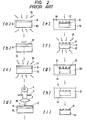
- Figure 2 is a flow chart showing an example of a process for fabricating the reticle pattern.
- a sample (reticle substrate) 8 in which a shading material 9 is deposited on a transparent glass substrate 10 is subjected to baking prior to coating with a resist.
- the resist material is dropped thereonto so as to form a uniform resist film 17 on the shading material 9.
- the sample 8 is prebaked with the thermal beam 16 again.
- the resist latent image 18 of a desired pattern is formed as shown in (d) by the use of the pattern generator explained with reference to Figure 1.
- the resist latent image pattern formed by the pattern generator is treated with a resist developer 19, thereby to develop the resist pattern 17.
- the developed pattern is fixed with a rinse, and the resultant sample is post-baked with the thermal beam 16 as shown in (f).
- the shading material 9 is chemically etched with an etchant 20 so as to form the pattern of the shading material 9.
- the sample is washed with water, and the resist pattern 17 is removed with a resist stripper 21 as shown in (h).
- the resultant sample is washed with water and dried. Then, the fabrication of the reticle made up of the shading material pattern 9 and the glass substrate 10 as shown in (i) is finished.
- the prior-art process has the disadvantage that large numbers of thermal treatment and chemical treatment steps are necessary.
- the reticle fabricating steps other than the foregoing step of forming the resist latent image pattern take a long period of wasteful time.
- the period of time for the series of thermal and chemical treatments at least 2 hours are required.
- improvements in or omission of such attendant processing steps have/has become important.
- US-A-4,190,759 discloses a pattern generator exhibiting the features of the precharacterising part of claim 1. While this known pattern generator makes it possible, due to the fact that it employs a laser beam for machining the pattern, to produce the pattern with a reduced number of processing steps and without employing a resist material, problems have been noted in that the edge of the pattern machined bulges into a lip formation, that the substrate and shading material have a tendency to fuse together, and that the substrate is damaged. These problems, which impair the precision of the pattern produced, result from a dissolution of the shading material and are ascribable to the influence of surface tension, chemical reaction of the material with oxygen in the atmosphere, etc.
- the shading material fulfilling the above prerequisites is, for example, chromium (Cr) which causes sublimation at a degree of vacuum on the order of 1.3 Pa.
- a laser beam 24 emitted from a high power laser source 22 enters a laser beam deflector 25 via a laser beam modulator 23, and it is deflected in at least one of the x and y directions. After the deflection, the laser beam 24 is turned by a mirror 26 and is focussed by a focussing lens 27 onto a film to-be-machined 29 formed on the upper surface of a transparent glass substrate 30 in a sample 28. Thus, the direct machining of the film to-be-machined 29 is performed.
- the laser source 22 employed here signifies a continuous-wave laser source such as argon ion laser or a pulse laser source such as excimer laser.
- the laser beam modulator 23 there is employed an acoustooptical device, an electro- optical device, a mechanical modulator or the like. When the pulse laser source is used, the laser beam modulator may be sometimes omitted.
- Used as the laser beam deflector 25 is a mechanical one employing a polygon mirror or galvanometer, or one employing an acoustooptical device or the like. It deflects the laser beam in at least one axial direction.
- the laser beam 24 is fined into a very small spot diameter, and hence, the focal depth becomes small.
- the apparatus is therefore controlled so that the focusing position may be held fixed by means of a Z-direction moving mechanism for a movable stage installed in vacuum.
- a detection mechanism for the Z-direction position of the film to-be-machined 29 is not illustrated in the figure, this position is detected by a known, pattern dimension measuring method employing a laser beam or the like method, and the spacing between the focusing lens 27 and the film to-be-machined 29 is held constant by the Z-direction moving mechanism, to be described later, which responds to the resulting detection signal.
- the whole movable stage, on which the sample 28 is placed, has a structure wherein an X-direction stage 35 and a Y-direction stage 34 are carried on a stationary base 36 and wherein a sample holder 32 carrying a mirror 31 for laser measurement is stacked on the Y-direction stage 34 through a wedge 33 for Z-direction movement, the holder 32 being movable in X-, Y- and Z-directions.
- the Z-direction drive is executed by moving the wedge 33 horizontally to drive the holder 32 in the Z-direction (along the optic axis) by means of a Z-direction driving motor 38 and feed screw 39.
- the X-direction stage 35 is driven by an X-direction driving motor 40 and through an X-direction feed screw 41, and it is positioned to a destination address or continuously moved at a constant speed in the X-direction.
- the drive of the Y-direction stage 34 is similarly performed.
- the position of the holder 32 in the X-direction is detected by a laser measurement equipment 44.
- This laser measurement equipment 44 may be, for example, one utilizing a known laser interferometer or a conventional length measuring instrument based on the moire method.
- the positional detection in the Y-direction is performed similarly to the above.
- the Z-direction movement can be made, not only by the system employing the wedge 33 shown in the present embodiment, but also by means employing a piezoelectric device or by an electromagnetic driver such as voice coil.
- the whole movable stage is installed within a vacuum chamber 43, the interior of which is evacuated through an evacuating port 37.
- Numeral 42 designates a viewing port for laser measurement.
- the sample 28 is such that the film to-be-machined 29 made of chromium or the like is deposited on the transparent glass substrate 30. This sample is installed on the holder 32.
- the control system of the present pattern generator is chiefly composed of a computer 45, a data processor 46 and the laser measurement equipment 44.
- the laser beam modulator 23, laser beam deflector 25, stage driving motor 40 (only the X-direction driving motor is shown in the figure) and laser measurement equipment 44 are controlled by the computer 45 and data processor 46 so as to directly machine the desired IC pattern on the film 29 with the laser.
- Figures 4A and 4B elucidate a pattern making method based on the raster scanning attended with the continuous drive of the movable stage.
- the laser beam 24 is scanned in the direction of arrows 47 within a specified range of the surface of the film to-be-machined 29, to successively and continuously move in directions 101, 102, 103, 104,105,106 and 107 and to directly machine the desired laser-machining range of the sample 28.
- the embodiment stated above is so constructed that the sample and the whole movable sample stage, on which the sample is placed, are installed within the vacuum vessel.
- the whole movable stage need not always be put in vacuum, but it suffices for the direct machining with the laser beam that at least the workpiece is situated in vacuum.
- Figure 5 is a schematic view showing an embodiment for such aspect of performance. It is sufficient for the laser machining of this invention that at least the workpiece lies in vacuum, and not only the construction shown in Figure 3, but also a construction shown in Figure 5 can be employed.
- a vacuum vessel 49 having an evacuating pipe 48' is mounted on X-, Y- and Z-direction stages (35, 34 and 50) disposed on the stationary base 36, the sample 28 is installed so that the film to-be-machined 29 made of the shading material such as chromium may face the side of the vacuum chamber 53 of the vacuum vessel, and the film 29 is directly machined with the laser beam having penetrated through the glass substrate 30.
- the shading material such as chromium
- the vacuum vessel 49 has a sealing member, such as O-ring, 51 interposed between it and the sample 28 itself. Thus, it shields the interior 53 from the atmosphere and holds it in a vacuum state. In this way, the laser beam 24 is permitted to fall on the film to-be-machined 29 held in the vaccuum chamber, through the glass substrate 30 and to machine the film. Owing to such construction, the vapor 47' of molecules or atoms emitted from the film to-be-machined 29 during the laser machining is evaporated on the inner wall of the vessel 49. This brings forth the additional effect that the focusing lens 27 can be prevented from being contaminated with the vaporized substance.
- a sealing member such as O-ring
- FIG. 6 is a schematic view showing still another embodiment of this invention.
- a sample table 55 having a hollow space 52 is mounted on the X-, Y- and Z-direction stages (35, 34 and 50), the sample 28 is installed thereon so that the film to-be-machined 29 may face the side opposite to the focusing lens 27 as in Figure 5, the sample 28 is fixed onto the sample table 55 by a sample holder 54, and the film 29 is directly machined with the laser beam having penetrated through the glass substrate 30.
- the embodiment of Figure 6 can protect the focusing lens 27 against the contamination with the vaporized substance 47 from the film to-be-machined 29.
- the sample fixing and holding mechanism in Figure 6 not only the mechanical means as illustrated, but also an electrostatic chuck mechanism which exploits the conductivity of such metal as chromium constituting the film to-be-machined 29, etc. can be used.
- stage driving system the laser measurement system, the control system etc. have been omitted from the description of the embodiments shown in Figures 5 and 6, it is needless to say that the same arrangements as explained in the embodiment shown in Figure 3 can be applied thereto.
- Any of the foregoing embodiments has been exemplified as employing the so-called lateral laser optical system which runs parallel to the horizon and in which the laser beam is bent by the mirror. Needless to say, however, this invention is not restricted thereto, but the so-called vertical laser optical system which runs at right angles to the horizon is applicable without any difficulty.
- a laser beam can be deflected at high resolution and at high speed. It is therefore permitted to prepare a complicated pattern such as an IC pattern at higher precision and at higher speed than in the prior-art pattern generator. Further, owing to the direct laser machining, there can be omitted the step of developing a resist, the step of etching a shading metal film, etc. as involved in the prior art, and the fabrication time of the IC pattern can be sharply shortened.
- the laser machining is performed in vacuum, the oxidation of a film to-be-machined is suppressed, the thermal diffusion is reduced, and the boiling point and melting point of the film become close or are inverted in the relation of magnitude, resulting in causing sublimation.
- the shape of the machined pattern is improved, and the machining speed of the pattern by the laser beam is raised by lowering the vaporizing-temperature.
- the pattern of a complicated IC can be directly machined in the same extent of short time as in case of employing an electron-beam lithographic system. This renders the fabrication of the IC pattern much higher in speed because all thermal and chemical treatments required in the electron-beam lithography can be excluded.
- the reticle fabricating technique of this invention is combined with the reduction projection and exposure technique, the process of an IC pattern till the printing thereof on a wafer can be executed in a very short time on the basis of the data of the pattern. Accordingly, this invention can be effectively utilized for the development of semiconductor devices and for the multikind and small quantity production.
Landscapes
- Engineering & Computer Science (AREA)
- Physics & Mathematics (AREA)
- Optics & Photonics (AREA)
- Plasma & Fusion (AREA)
- Mechanical Engineering (AREA)
- General Physics & Mathematics (AREA)
- Health & Medical Sciences (AREA)
- Atmospheric Sciences (AREA)
- Life Sciences & Earth Sciences (AREA)
- Toxicology (AREA)
- Environmental & Geological Engineering (AREA)
- Epidemiology (AREA)
- Public Health (AREA)
- Exposure And Positioning Against Photoresist Photosensitive Materials (AREA)
- Exposure Of Semiconductors, Excluding Electron Or Ion Beam Exposure (AREA)
- Preparing Plates And Mask In Photomechanical Process (AREA)
Claims (5)
Applications Claiming Priority (2)
| Application Number | Priority Date | Filing Date | Title |
|---|---|---|---|
| JP177281/80 | 1980-12-17 | ||
| JP55177281A JPS57102016A (en) | 1980-12-17 | 1980-12-17 | Pattern generator |
Publications (3)
| Publication Number | Publication Date |
|---|---|
| EP0054315A2 EP0054315A2 (de) | 1982-06-23 |
| EP0054315A3 EP0054315A3 (en) | 1983-06-22 |
| EP0054315B1 true EP0054315B1 (de) | 1986-08-20 |
Family
ID=16028290
Family Applications (1)
| Application Number | Title | Priority Date | Filing Date |
|---|---|---|---|
| EP81110558A Expired EP0054315B1 (de) | 1980-12-17 | 1981-12-17 | Herstellung von Masken |
Country Status (5)
| Country | Link |
|---|---|
| US (1) | US4504726A (de) |
| EP (1) | EP0054315B1 (de) |
| JP (1) | JPS57102016A (de) |
| CA (1) | CA1175958A (de) |
| DE (1) | DE3175181D1 (de) |
Families Citing this family (33)
| Publication number | Priority date | Publication date | Assignee | Title |
|---|---|---|---|---|
| USRE33931E (en) * | 1981-12-21 | 1992-05-19 | American Semiconductor Equipment Technologies | Laser pattern generating system |
| US4493967A (en) * | 1982-09-01 | 1985-01-15 | Westinghouse Electric Corp. | Rigid support for laser machining apparatus |
| US4718418A (en) * | 1983-11-17 | 1988-01-12 | Lri L.P. | Apparatus for ophthalmological surgery |
| DE3427611A1 (de) * | 1984-07-26 | 1988-06-09 | Bille Josef | Laserstrahl-lithograph |
| JPS61111563A (ja) * | 1984-11-05 | 1986-05-29 | Mitsubishi Electric Corp | 半導体装置の金属配線切断方法 |
| US4642438A (en) * | 1984-11-19 | 1987-02-10 | International Business Machines Corporation | Workpiece mounting and clamping system having submicron positioning repeatability |
| JPS61244030A (ja) * | 1985-04-22 | 1986-10-30 | Nec Corp | パタ−ンジエネレ−タ |
| US4752668A (en) * | 1986-04-28 | 1988-06-21 | Rosenfield Michael G | System for laser removal of excess material from a semiconductor wafer |
| US4801352A (en) * | 1986-12-30 | 1989-01-31 | Image Micro Systems, Inc. | Flowing gas seal enclosure for processing workpiece surface with controlled gas environment and intense laser irradiation |
| US5221422A (en) * | 1988-06-06 | 1993-06-22 | Digital Equipment Corporation | Lithographic technique using laser scanning for fabrication of electronic components and the like |
| US5014207A (en) * | 1989-04-21 | 1991-05-07 | E. I. Du Pont De Nemours And Company | Solid imaging system |
| US4940508A (en) * | 1989-06-26 | 1990-07-10 | Digital Equipment Corporation | Apparatus and method for forming die sites in a high density electrical interconnecting structure |
| JPH03180413A (ja) * | 1989-12-08 | 1991-08-06 | Nkk Corp | 竪型炉の装入物傾斜角制御装置 |
| US5656229A (en) * | 1990-02-20 | 1997-08-12 | Nikon Corporation | Method for removing a thin film layer |
| DE59103714D1 (de) * | 1991-10-07 | 1995-01-12 | Siemens Ag | Laserbearbeitungsverfahren für einen Dünnschichtaufbau. |
| US5643801A (en) * | 1992-11-06 | 1997-07-01 | Semiconductor Energy Laboratory Co., Ltd. | Laser processing method and alignment |
| US5558789A (en) * | 1994-03-02 | 1996-09-24 | University Of Florida | Method of applying a laser beam creating micro-scale surface structures prior to deposition of film for increased adhesion |
| DE19529656B4 (de) * | 1995-08-11 | 2007-01-04 | Heidelberg Instruments Mikrotechnik Gmbh | Verfahren zur Herstellung von Mikrostrukturen |
| CA2278578A1 (en) * | 1997-11-28 | 1999-06-10 | Tsuneo Mitsuyu | Method and device for activating semiconductor impurities |
| SG90732A1 (en) * | 1999-06-30 | 2002-08-20 | Canon Kk | Laser processing method, method for manufacturing ink jet recording head using such method of manufacture, and ink jet recording head manufactured by such method of manufacture |
| US6615481B1 (en) * | 2000-06-08 | 2003-09-09 | Nikon Corporation | Method for fabrication of electromagnetic coil vanes |
| SE518170C2 (sv) * | 2000-06-27 | 2002-09-03 | Micronic Laser Systems Ab | Flerstrålemönstergenerator och metod för skannande |
| DE10050263A1 (de) * | 2000-10-09 | 2002-04-18 | Rodenstock Optik G | Verfahren zur Kennzeichnung und insbesondere zur Beschriftung von Oberflächen optischer Elemente mit UV-Licht |
| US6649529B2 (en) * | 2001-08-15 | 2003-11-18 | Intel Corporation | Method of substrate processing and photoresist exposure |
| FI20041515L (fi) * | 2004-11-25 | 2006-05-26 | Lasermark Ab Oy | Menetelmä lääketieteellisten stenttien valmistamiseksi |
| US8426250B2 (en) * | 2008-10-22 | 2013-04-23 | Intel Corporation | Laser-assisted chemical singulation of a wafer |
| US20100129984A1 (en) * | 2008-11-26 | 2010-05-27 | George Vakanas | Wafer singulation in high volume manufacturing |
| CN102510788B (zh) * | 2010-06-14 | 2014-12-24 | 三菱电机株式会社 | 激光加工装置以及激光加工方法 |
| GB2499594B (en) * | 2012-02-21 | 2020-05-06 | Aquasium Tech Limited | Laser welding method and apparatus |
| US10672603B2 (en) | 2015-10-23 | 2020-06-02 | Infineon Technologies Ag | System and method for removing dielectric material |
| US11890807B1 (en) | 2017-08-31 | 2024-02-06 | Blue Origin, Llc | Systems and methods for controlling additive manufacturing processes |
| US11819943B1 (en) * | 2019-03-28 | 2023-11-21 | Blue Origin Llc | Laser material fusion under vacuum, and associated systems and methods |
| CN110369865A (zh) * | 2019-08-12 | 2019-10-25 | 湖南城市学院 | 一种用于激光焊接的密封装置 |
Family Cites Families (9)
| Publication number | Priority date | Publication date | Assignee | Title |
|---|---|---|---|---|
| GB1138084A (en) * | 1966-07-22 | 1968-12-27 | Standard Telephones Cables Ltd | Method of vapour depositing a material in the form of a pattern |
| DE1572642A1 (de) * | 1967-06-26 | 1970-03-26 | Euratom | Laser-Bestrahlungsvorrichtung |
| FR2135425B1 (de) * | 1971-05-04 | 1973-08-10 | Thomson Csf | |
| US3889272A (en) * | 1974-05-30 | 1975-06-10 | Bell Telephone Labor Inc | Metal film recording media for laser writing |
| US4316073A (en) * | 1974-11-14 | 1982-02-16 | Lemelson Jerome H | Document recording method |
| US4190759A (en) * | 1975-08-27 | 1980-02-26 | Hitachi, Ltd. | Processing of photomask |
| US4215694A (en) * | 1978-06-01 | 1980-08-05 | Isakov Viktor L | Laser therapy apparatus |
| US4328410A (en) * | 1978-08-24 | 1982-05-04 | Slivinsky Sandra H | Laser skiving system |
| US4278867A (en) * | 1978-12-29 | 1981-07-14 | International Business Machines Corporation | System for chip joining by short wavelength radiation |
-
1980
- 1980-12-17 JP JP55177281A patent/JPS57102016A/ja active Pending
-
1981
- 1981-12-04 US US06/327,627 patent/US4504726A/en not_active Expired - Fee Related
- 1981-12-09 CA CA000391814A patent/CA1175958A/en not_active Expired
- 1981-12-17 DE DE8181110558T patent/DE3175181D1/de not_active Expired
- 1981-12-17 EP EP81110558A patent/EP0054315B1/de not_active Expired
Also Published As
| Publication number | Publication date |
|---|---|
| EP0054315A2 (de) | 1982-06-23 |
| EP0054315A3 (en) | 1983-06-22 |
| CA1175958A (en) | 1984-10-09 |
| DE3175181D1 (en) | 1986-09-25 |
| US4504726A (en) | 1985-03-12 |
| JPS57102016A (en) | 1982-06-24 |
Similar Documents
| Publication | Publication Date | Title |
|---|---|---|
| US4504726A (en) | Pattern generator | |
| EP0678768B2 (de) | Projektionsbelichtungsgerät und Herstellungsverfahren für eine Mikrovorrichtung | |
| EP1039511A1 (de) | Verfahren zur projektionsbelichtung und projektionsausrichteinrichtung | |
| US4310743A (en) | Ion beam lithography process and apparatus using step-and-repeat exposure | |
| US20080198467A1 (en) | Standard Component For Length Measurement, Method For Producing The Same, and Electron Beam Metrology System Using The Same | |
| US7038762B2 (en) | Method and apparatus for irradiating a microlithographic substrate | |
| Chan et al. | Development and applications of a laser writing lithography system for maskless patterning | |
| Koronkevich et al. | Fabrication of diffractive optical elements by direct laser-writing with circular scanning | |
| JP2019086709A (ja) | 露光システム、露光方法、及び表示用パネル基板の製造方法 | |
| US5023462A (en) | Photo-cathode image projection apparatus for patterning a semiconductor device | |
| JPH07105323B2 (ja) | 露光方法 | |
| JP3097620B2 (ja) | 走査型縮小投影露光装置 | |
| US6163368A (en) | Method and apparatus for performing a double shift print on a substrate | |
| JPH0855785A (ja) | 露光方法とこれを用いたデバイス製造方法 | |
| US8119312B2 (en) | Manufacturing method for a semiconductor device | |
| KR940010150B1 (ko) | 전자빔노광방법 및 그 장치 | |
| JP3187581B2 (ja) | X線装置、x線露光装置及び半導体デバイス製造方法 | |
| KR20050033078A (ko) | 피쳐 패턴 형성 방법, 레벨 단위 제조 방법 및 그 장치 | |
| TWI868413B (zh) | 描繪裝置、描繪系統以及描繪方法 | |
| JP3091821B2 (ja) | 露光装置およびデバイス製造方法 | |
| KR102544422B1 (ko) | 광학 투영을 이용한 기판 튜닝 시스템 및 방법 | |
| JP2019090961A (ja) | 露光装置 | |
| JP2000100758A (ja) | ビーム描画装置及びパターン形成方法 | |
| USH1463H (en) | Method for detecting positions of photomask and substrate | |
| US6278123B1 (en) | Reducing the critical dimension difference of features printed on a substrate |
Legal Events
| Date | Code | Title | Description |
|---|---|---|---|
| PUAI | Public reference made under article 153(3) epc to a published international application that has entered the european phase |
Free format text: ORIGINAL CODE: 0009012 |
|
| 17P | Request for examination filed |
Effective date: 19811223 |
|
| AK | Designated contracting states |
Designated state(s): DE FR GB NL |
|
| PUAL | Search report despatched |
Free format text: ORIGINAL CODE: 0009013 |
|
| AK | Designated contracting states |
Designated state(s): DE FR GB NL |
|
| GRAA | (expected) grant |
Free format text: ORIGINAL CODE: 0009210 |
|
| AK | Designated contracting states |
Kind code of ref document: B1 Designated state(s): DE FR GB NL |
|
| REF | Corresponds to: |
Ref document number: 3175181 Country of ref document: DE Date of ref document: 19860925 |
|
| ET | Fr: translation filed | ||
| PLBE | No opposition filed within time limit |
Free format text: ORIGINAL CODE: 0009261 |
|
| STAA | Information on the status of an ep patent application or granted ep patent |
Free format text: STATUS: NO OPPOSITION FILED WITHIN TIME LIMIT |
|
| 26N | No opposition filed | ||
| PGFP | Annual fee paid to national office [announced via postgrant information from national office to epo] |
Ref country code: FR Payment date: 19921221 Year of fee payment: 12 |
|
| PGFP | Annual fee paid to national office [announced via postgrant information from national office to epo] |
Ref country code: DE Payment date: 19930225 Year of fee payment: 12 |
|
| PGFP | Annual fee paid to national office [announced via postgrant information from national office to epo] |
Ref country code: GB Payment date: 19931207 Year of fee payment: 13 |
|
| PGFP | Annual fee paid to national office [announced via postgrant information from national office to epo] |
Ref country code: NL Payment date: 19931231 Year of fee payment: 13 |
|
| PG25 | Lapsed in a contracting state [announced via postgrant information from national office to epo] |
Ref country code: FR Effective date: 19940831 |
|
| PG25 | Lapsed in a contracting state [announced via postgrant information from national office to epo] |
Ref country code: DE Effective date: 19940901 |
|
| REG | Reference to a national code |
Ref country code: FR Ref legal event code: ST |
|
| PG25 | Lapsed in a contracting state [announced via postgrant information from national office to epo] |
Ref country code: GB Effective date: 19941217 |
|
| PG25 | Lapsed in a contracting state [announced via postgrant information from national office to epo] |
Ref country code: NL Effective date: 19950701 |
|
| GBPC | Gb: european patent ceased through non-payment of renewal fee |
Effective date: 19941217 |
|
| NLV4 | Nl: lapsed or anulled due to non-payment of the annual fee |
Effective date: 19950701 |