EP0054323B1 - Déphaseur pour impulsions d'horloge - Google Patents
Déphaseur pour impulsions d'horloge Download PDFInfo
- Publication number
- EP0054323B1 EP0054323B1 EP81201295A EP81201295A EP0054323B1 EP 0054323 B1 EP0054323 B1 EP 0054323B1 EP 81201295 A EP81201295 A EP 81201295A EP 81201295 A EP81201295 A EP 81201295A EP 0054323 B1 EP0054323 B1 EP 0054323B1
- Authority
- EP
- European Patent Office
- Prior art keywords
- phase
- signal
- transistor
- pairs
- control
- Prior art date
- Legal status (The legal status is an assumption and is not a legal conclusion. Google has not performed a legal analysis and makes no representation as to the accuracy of the status listed.)
- Expired
Links
- 230000010363 phase shift Effects 0.000 claims description 44
- 239000003990 capacitor Substances 0.000 claims description 18
- 238000010079 rubber tapping Methods 0.000 claims description 14
- 230000004044 response Effects 0.000 claims description 13
- 230000008859 change Effects 0.000 claims description 7
- 238000004519 manufacturing process Methods 0.000 claims description 4
- 230000005540 biological transmission Effects 0.000 description 18
- 238000010586 diagram Methods 0.000 description 12
- 239000013598 vector Substances 0.000 description 11
- 230000007423 decrease Effects 0.000 description 5
- 230000000694 effects Effects 0.000 description 5
- 239000013078 crystal Substances 0.000 description 3
- 230000008901 benefit Effects 0.000 description 2
- 238000001514 detection method Methods 0.000 description 2
- 230000005669 field effect Effects 0.000 description 2
- 238000009432 framing Methods 0.000 description 2
- 230000011664 signaling Effects 0.000 description 2
- 230000003247 decreasing effect Effects 0.000 description 1
- 230000006866 deterioration Effects 0.000 description 1
- 238000007599 discharging Methods 0.000 description 1
- 230000000977 initiatory effect Effects 0.000 description 1
- 238000000034 method Methods 0.000 description 1
- 230000010355 oscillation Effects 0.000 description 1
- 238000007493 shaping process Methods 0.000 description 1
- 230000001360 synchronised effect Effects 0.000 description 1
Images

Classifications
-
- H—ELECTRICITY
- H03—ELECTRONIC CIRCUITRY
- H03H—IMPEDANCE NETWORKS, e.g. RESONANT CIRCUITS; RESONATORS
- H03H11/00—Networks using active elements
- H03H11/02—Multiple-port networks
- H03H11/16—Networks for phase shifting
- H03H11/20—Two-port phase shifters providing an adjustable phase shift
-
- H—ELECTRICITY
- H03—ELECTRONIC CIRCUITRY
- H03H—IMPEDANCE NETWORKS, e.g. RESONANT CIRCUITS; RESONATORS
- H03H17/00—Networks using digital techniques
- H03H17/08—Networks for phase shifting
Definitions
- This invention relates to a data pulse receiver arrangement of a type suitable for the acquisition of data pulses which occur in a serial bit stream in a received information signal in which one level of the signal (say high) represents a binary value '1' and another of the signal (say low) represents a binary value '0', said arrangement including a data clock pulse generator for clocking the data pulses into the data pulse receiver arrangement.
- the invention relates more particularly to a phase shifter in or for use in such data clock pulse generator.
- a data pulse receiver arrangement of the above type (which is known for instance from Mullard Technical Information No. 34, dated September 1976, and Mullard Technical Information No. 54, dated August 1977) has application in data transmission systems in which data transmission and reception is not synchronised.
- a data transmission system is for example, the BBC/IBA Teletext television transmission system in which coded data pulses representing alphanumeric text or other message information are transmitted in a video signal in at least one television line in field-blanking intervals where no picture signals representing normal picture information are present.
- United Kingdom Patent Specification No. 1,370,535 discloses a television transmission system of this form.
- a difficulty that occurs with such an application of the data pulse receiver arrangement is to synchronise clock pulses locally generated therein with the received data pulses.
- One technique for achieving this synchronisation is to generate a local data pulse clock independently of the received data pulses and then shift its phase into synchronism with them.
- a data clock pulse generator which is suitable for this purpose may comprise an oscillator arranged for oscillation at a predetermined frequency to produce locally generated clock pulses, together with a phase sensitive detector which is operable to produce a control signal in accordance with the relative phases of the received data pulses and the clock pulses, which control signal is then used to correct the phase of the oscillator output signal to bring the data pulses and clock pulses into synchronism.
- the control exercised by the control signal may act directly on the oscillator (e.g. in the case of a voltage-controlled oscillator), so that the phase of the oscillator output signal, as actually produced, ts corrected.
- the control exercised by the control signal may cause a phase shifter to alter the phase of the oscillator output signal after it has been produced.
- This latter form of control permits a highly stable oscillator, such as a crystal-controlled oscillator, to be used to generate the clock pulses, but it requires the use of a phase shifter which can produce a large accurate phase shift.
- phase shifter is of a character comprising phase quadrature means for producing in phase quadrature first and second signal versions of the single frequency signal, function generator means responsive to a control signal representative of a required phase shift to produce first and second control factors, multiplier means operable to multiply said first and second signal versions by said first and second control factors, respectively, to produce resultant first and second signal versions in phase quadrature having respective controlled amplitudes, and combining means for combining said first and second resultant signal versions to produce an output signal which is a phase shifted version of said (original) single frequency signal, the controlled amplitudes of said resultant signal versions determining the phase of the output signal.
- the output signal (x cos wt+y sin wt) can be expressed as A sin (wt+8), where 0 is the required phase shift.
- phase shift (8) lie anywhere between 0° and 360° can be achieved by so arranging the function generator means so that the controlled amplitude (x and y) are made positive or negative, selectively, so that 8 lies in one of the four quadrants 0° to 90°, 90° to 180°, 180° to 270° and 270° to 360°.
- a phase shifter of the above character is characterised by further comprising capacitor means for storing said control signal and additional means associated with said function generator means and responsive to a first range of values of the control signal to cause the production by the function generator means for said first and second control factors in respect of a first phase shift between 0° and 360°, said additional means being thereafter responsive to at least one further range of values of the control signal to cause the production by the function generator means of said first and second control factors in respect of one or more further phase shifts between 0° and 360°, whereby the total phase shift 0 can extend over a number of complete cycles of the single frequency signal.
- the phase shifter may be so arranged that the first and second signal versions as produced by the phase quadrature means comprise respective pairs of anti-phase signals, that the first and second control factors are control currents which are produced by a current generator, which constitutes the function generator means, as respective pairs of oppositely poled currents of which the difference between the two currents of each pair represents the relevant control current, and that said multiplier means comprises a first four quadrant multiplier for producing said first resultant signal version in response to one of said pairs of anti-phase signals and one of said pairs of oppositely poled currents and a second four quadrant multiplier for producing said second resultant signal version in response to the other of said pairs of anti-phase signals and the other of said pairs of oppositely poled currents.
- Said current generator can comprise a plurality of transistor pairs each having first and second transistors connected in a long-tailed configuration in which their emitters are coupled to a current source via respective emitter resistances, which transistor pairs are arranged in two sets that provide said respective pairs of oppositely poled currents at respective pairs of positive and negative output terminals; in which two sets the base of the first transistor of each pair is connected to receive a control voltage which consitutes said control signal and the base of the second transistor of each pair is connected to a respective tapping point of a potential divider, which tapping points as considered in their order of potential have bases of the second transistors from one set and the other connected to them alternately; and in each set the collectors of the first transistors of successive transistor pairs are connected to the positive output terminal and the negative output terminal alternately, and likewise their second transistor collectors are connected to these terminals alternately, the arrangement being such that for a given value of control voltage lying between the potentials of two immediately adjacent tapping points, those transistor pairs having their second transistor bases connected to respective other tapping points have one transistor fully
- Each of said sets comprises two transistor pairs, for each phase shift in the range 0° to 360°, so that for a phase shift range covering a number of complete cycles in accordance with the present invention each set would have an appropriate number of transistor pairs constituting said additional means.
- each transistor pair can provide a phase shift of 90° maximum.
- said additional means can comprise first means which, each time the control signal reaches one of two spaced limit values, is operable to reverse the operating sense of the phase shifter in its utilisation of said first and second control factors, together with second means for causing an associated phase sensitive detector which produces the control signal to reverse the sense that the control signal changes value in response to detected phase variation, the successive excursions of the control signal between said two limit values forming said first and further ranges of values thereof.
- a phase shifter in accordance with the present invention can, in principle, achieve a phase shift of so many successive cycles that an effective small change (i.e. increase or decrease) in the frequency of the single frequency signal can be produced.
- This facility of effecting a small frequency change is particularly advantageous in a contemplated application of the present invention in the generation of a local data pulse clock for clocking data pulses into a data pulse receiver arrangement from different data sources such as, for instance, an over-air Teletext broadcast transmission on the one hand, and a video cassette recorder (VCR) or other form of local data store in which previously transmitted Teletext data has been recorded, on the other hand.
- VCR video cassette recorder
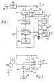
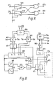
- the data clock pulse generator shown in Figure 1 has a specific application in a data pulse receiver arrangement for the aforesaid BBC/IBA Teletext television transmission system.
- This data clock pulse generator includes a data clock pulse source 101, a phase sensitive detector 102 and a storage capacitor 103.
- a data slicer 104 receives data pulses DP from an input terminal 105. After level correction and possibly re-shaping (by suitable known means not shown), the data pulses DP are applied to an output lead 106 for utilisation in further circuitry, the pulses DP being clocked into this further circuitry by means of clock pulses CK which are applied to a clock pulse lead 107 by the source 101.
- the data pulses DP and clock pulses CK are also applied to the phase sensitive detector 102 which is responsive thereto to produce a control signal CS on a control lead 108, this control signal CS having a value in accordance with the relative phase of the data pulses DP and the clock pulses CK.
- the source 101 comprises a crystal-controlled oscillator 109 and a phase shifter 110.
- the oscillator 109 produces a highly stable alternating signal at the clock frequency and the phase shifter 110 is responsive in accordance with the value of a control voltage across the capacitor 103 to bring the oscillator output signal into phase synchronism with the data pulses DP.
- the control voltage constitutes the final form of the control signal CS, as will be described.
- a limiter 111 is provided for limiting (and squaring) the output signal from the source 101.
- the data clock pulse generator of Figure 1 additionally comprises a voltage-to-current converter 112, a timing circuit 113 and a re-setting circuit 114, which are all involved in the establishment of the appropriate control voltage across the capacitor 103.
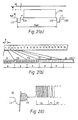
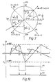
- FIG. 2(a) shows a waveform diagram which represents a Teletext television video signal for one television line which occurs in a field-blanking interval and which includes coded pulse data.
- the line synchronising pulse for the television line concerned is represented at LS1
- the line synchronising pulse for the next television line is represented at LS2.
- the colour burst on the television line concerned and that on the next televison line, are represented at CB1 and CB2, respectively.
- the period of one television line i.e. the period between the leading edges of successive line synchronising pulses
- the standards adopted in the United Kingdom for information transmission by digitally coded pulses in the field-blanking intervals of such a 625-line system see "Broadcast Teletext Specification", September 1976, published jointly by the British Broadcasting Corporation, Independent Broadcasting Authority and British Radio Equipment Manufacturer's Association), then the television line shown would be line number 17 or 18 in an even field or line number 330 or 331 in an odd field.
- Such a television line is referred to as a television data line and can contain coded pulse data representing 360 binary bits which may be considered as 45 eight-bit bytes.
- the position of the coded pulse data in the data line is indicated at CPD.
- the binary bit signalling rate is approximately 7 Mbit/s, and the binary bit signalling levels are defined between a black level BL and a peak white level WL.
- the binary '0' level is the level BL and the binary '1' level is the level L.
- Figure 2(b) shows a possible format for coded pulse data in a television data line.
- the binary bits representing the coded pulse data are divided up into eight-bit bytes 1, 2, ... 20 ...
- the first two bytes 1 and 2 comprise a sequence of clock run-in pulses which in the present example consist of a sequence of alternating bits 10101010/10101010.
- the third byte 3 comprises a framing or start code, e.g. 11100100, which a data pulse receiver arrangement has to identify before it will respond to accept message information which is contained in the remaining eight-bit bytes 4, 5, ... 20....
- Figure 2(c) shows in idealised form the first part of a video signal waveform VS for a television data line showing the sequence of clock run-in pulses CL and the sequence of pulses which comprise the framing code FR.
- the first few coded data pulses which represent alpha-numeric characters or other message information are shown at DP.
- the line synchronising pulse is represented at LS and the colour burst at CB.
- the re-setting circuit 114 is so organised in relation to the coded data pulse transmission format described above with reference to Figures 2a to 2c, that in each television data line it is operated by the line flyback pulse FL to connect a reference voltage RV across the capacitor 103 during the line blanking interval.
- This reference voltage RV sets the voltage across the capacitor 103 to a value corresponding to the centre or other selected position of its control range; that is, of the phase range afforded by the phase shifter 110.
- the re-setting circuit 114 can simply comprise, as indicated, a field-effect transistor which is arranged as an electronic switch to connect the reference voltage RV across the capacitor 103 during the application of the flyback pulse FL to its gate electrode.
- the timing circuit 113 supplies to the voltage-to-current converter 112 a timing pulse T which causes the converter 112 to substantially increase (e.g. double) its current output from a normal rate at which it functions in response to the control signal CS (which it receives as a voltage), so that within this relatively short clock run-in period the control voltage across the capacitor 103 as produced by the current output of the converter 112 can assume in respect of the television data line a starting value corresponding to the mean phase of the sequence of clock run-in pulses CL.
- the converter 112 operates to produce its current output at the normal, lower, rate to provide a more stable control voltage for the code pulses which follow the clock run-in pulses.
- the initial higher rate of control voltage variation during the clock run-in period enables a reliable starting value for the control voltage to be obtained for satisfactory phase correction in respect of the code pulses. Without this initial action, there may be insufficient time to correct adequately for phase drift between the data pulses and the clock pulses from one television data line to the next.
- the timing circuit 113 For producing the timing pulse T the timing circuit 113 comprises a line synchronising pulse separator 115 and a pulse generator 116.
- the synchronising pulse separator 115 detects the line sync. Pulses LS in the video signal VS to trigger the pulse generator 116 which is responsive to produce the timing pulse T.
- the pulse generator 116 includes a trigger delay such that the timing pulse T occurs at the beginning of the sequence of clock pulses CL and last for substantially the duration thereof.
- the data slicer 104, the limiter 111 and the crystal-controlled oscillator 109 can take any suitable known form. As regards the implementation of the phase sensitive detector 102 this can also take any suitable known form, but preferably, it is implemented as set forth in our co-pending European Patent Application No. 81201294.6.
- the converter 112 in Figure 1 preferably takes the form shown in Figure 3, wherein it comprises two current sources 301 and 302 and an electronic switch 303.
- the current source 301 comprises two transistor pairs 304/305 and 306/307 of opposite conductivity type, both pairs being connected as current mirrors.
- the transistors 305 and 307 are connected in push-pull with their collectors connected together and to the capacitor 103, which is the capacitor 103 of Figure 1.
- the collectors of the other two transistors 304 and 306 are fed, respectively, with voltage pulses 308 and 309 of opposite polarity, which constitute the voltage output from the phase sensitive detector 102 in Figure 1. These voltage pulses are assumed to vary in width, in accordance with the difference in phase between the data pulses DP and the clock pulses CK.
- Two resistors 310 and 311 determine the current magnitude that flows in the transistors 304 and 306 in response to the voltage pulses 308 and 309.
- the resultant push-pull current in the transistors 305 and 307 adjusts the charge on the capacitor 103.
- the other current source 302 is provided to supply increased current into the capacitor circuit during the period of the clock run-in pulses CL.
- This current source 302 is the same as the source 301 in that it comprises two transistor pairs 312/313 and 314/ 315 of opposite conductivity type which are connected as current mirrors, with the transistors 313 and 315 connected in push-pull with their collectors connected together.
- this switch 303 comprises a field-effect transistor 316 which has the timing pulse T applied to its gate, so that the capacitor 103 receives current from this current source 302 only for the duration of this timing pulse T.
- the current due to the current source 302 is made proportionally different to that due to the first current source 301 by suitable selection of the values of resistors 317 and 318 relative to the values of the corresponding resistors 310 and 311 in the current source 301.
- the phase shifter 110 in Figure 1 can take the basic form shown in Figure 4.
- This basic form of phase shifter comprises a phase shifter network 401, two multipliers 402 and 403, a current generator 404 and an adder 405.
- the single frequency signal produced by the oscillator 109 is applied directly to one input 406 of the multiplier 402 and via the phase shifter network 401 to one input 407 of the multiplier 403.
- the network 401 provides a 90° phase shift, so that the two signal versions of the oscillator output signal are in phase quadrature.
- the current generator 404 has the control voltage V o across the capacitor 103 applied to it and is responsive thereto to produce two control currents which are applied respectively to respective second inputs 408 and 409 of the two multipliers 402 and 403.
- the two multipliers 402 and 403 reproduce the single frequency signal applied to their respective inputs 406 and 407 but with a controlled amplitude which is determined by the value of the respective control currents applied to their other inputs 408 and 409.
- These two resultant single frequency signals of controlled amplitude and in phase quadrature are applied to the adder 405 which is operable in response thereto to provide a phase shifted version of the original single frequency signal produced by the oscillator 109.
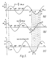
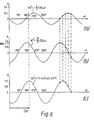
- the operation of the phase shifter shown in Figure 4 to produce a phase shift of 45° is illustrated by the waveform diagrams in Figure 5, and its operation to produce a phase shift of 210° is illustrated by the waveform diagrams in Figure 6.
- Figures 5a and 5b two single frequency waveforms and are shown. These two waveforms W1 and W2 are thus in phase quadrature and each has an amplitude of V2/2 current units A. If these two waveforms W1 and W2 are combined, then a resultant waveform is produced, as shown in Figure 5c, which has an amplitude of 1.0 current units A, and a phase shift of 45° in that it reaches its peak 45° along the horizontal axis wt.
- phase shifter shown in Figure 8 functions on the same principle as the basic form of phase shifter shown in Figure 1, and means are also provided therein for achieving a phase shift of more than 360°.
- an unlimited phase shift is possible so that an effective small change (i.e. increase or decrease) in the clock frequency can be produced.
- the facility of effecting a small clock frequency change can be particularly advantageous where data pulses are clocked into a data pulse receiver arrangement from a video cassette recorder, following receipt and storage of the data pulses from a broad Teletext transmission. This advantage is due to the fact that in the "retransmission" of the data pulses from the video cassette recorder, there can be a significant deterioration in the transmission standards compared with the original broadcast transmission.
- the phase shifter shown in Figure 8 comprises two multipliers 801 and 802, a current generator 803, a 90° phase shift network 804, an inverter 805 and an adder 806.
- This phase shifter additionally comprises, for achieving (unlimited) phase shifts greater than 360°, two limit detectors 807 and 808, an OR-gate 809, a divide-by-two circuit 810, and two polarity reversing switches 811 and 812.
- Figure 8 also shows an oscillator 813, an element 814 of a phase sensitive detector (such as set forth in our said co-pending Application) which produces current for the control voltage V o , and the capacitor 103 across which the control voltage V c is derived.
- the output signal CK of the oscillator 813 is applied directly to the phase shift network 804 and also to the inverter 805 whose output signal is also applied to the phase shift network 804.
- the oscillator output signal and the inverter output signal form one pair of anti-phase single frequency signals I ac , T ac and the two output signals from the phase shift network 804 form another pair of anti-phase single frequency signals Q ac , Q ac which are respectively in phase quadrature with the signals I ac , I ac .
- the multipliers 801 and 802 are respective four-quadrant multipliers (e.g.
- the signal pairs and current pairs are multiplied together to produce pairs of resultant output signals which are combined separately by the adder 806 to form two anti-phased and phase-shifted versions CLK and CLK of the original single frequency signal CK.
- the difference between each of the current pairs I c , I c and Q c , Q c is negative, so that modulation by I ac and Q ac , respectively, produces the vectors W1' and W2' which when combined produce W3'. (i.e. CLK with a 210° phase shift).
- CLK is also produced by combining the anti-phase versions of W1' and W2'.
- the control voltage V c has a predetermined operating range about a mean value, for example, a range of + volts to + volts about a mean value of 3 volts. Within this range it can be arranged such that when the control voltage V e is 3 volts, there is zero phase shift; and the phase shift varies progressively from 0° to +180° as the control voltage V e increases to volts and it varies progressively from 0° to-180° as the control voltage V c decreases to volts.
- the relevant limit detector 807 or 808 When either limit of the operating range is reached by the control voltage V c , the relevant limit detector 807 or 808 produces an output signal which is applied via the OR-gate 809 and the divide-by-two circuit 810 to operate the polarity reversing switches 811 and 812.
- phase sensitive detector (102- Figure 1)
- this output reversal can be achieved by switching the control inputs to the two current generators 815 and 816 which feed charging and discharging current to the capacitor 103.
- the vertical axis V c represents the control voltage V e and the horizontal axis represents time t.
- the line L1 shows that over the period t 1 to t 2 the phase is increasing (say) with increase in control voltage V c .
- the line L2 illustrates that for a phase shift of less than ⁇ 180°, the phase simply increases and decreases as the control voltage V e increases and decreases. In this instance the arrows across line L2 are alternately pointing upwards and downwards to signify the change in phase direction.
- the upper and lower limits V U and V L of the control voltage V c can be in respect of smaller phase ranges than ⁇ 180°; for instance, a phase range of ⁇ 90° or ⁇ 45° can be used. Also, larger phase ranges such as ⁇ 360° are possible.
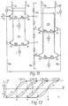
- FIG 11 shows a simplified circuit diagram of a current generator (404- Figure 4) and (803- Figure 8) employed in the phase shifter.
- This current generator comprises a plurality of pairs of transistors T1/T2, T3/T4, T5/T6 and T7/T8 connected in a long-tailed configuration. These transistor pairs are arranged in two sets S1 and S2 which provide the two pairs of oppositely poled currents I c , I c and Q c , Q c , respectively.
- Each of the transistor pairs has an individual (constant) current source i to which the emitters of the two transistors are connected via respective emitter resistances Ra and Rb. All the emitter resistances Ra and Rb are of the same value and all the current sources i are substantially the same as each other.
- Each of the two sets S1 and S2 also has a respective balance current source i a and i b which are also the same as the other current sources i. In practice, all the current sources would be comprised by respective transistor circuits.
- a potential divider PD having four tapping points a, b, c and d to which one transistor (i.e. T2, T4, T5 and T7) in each of the transistor pairs has its base connected, respectively.
- the other transistor (i.e. T1, T3, T6 and T7) in each of the transistor pairs has its base connected to an input terminal Vt to which the control voltage V c is applied.
- each of the current sources i (and i a and i b ) provides one unit of current.
- current vectors Wc and Wd each of magnitude would be generated when V e lies between b and c and between c and d, respectively.
- the presence of the emitter resistances Ra and Rb ensure that the current pairs I c and I c and Q c , Q e are actually produced with magnitudes that produce resultant current vectors such as W3 and W3' which lie approximately on the radius R and which can be at any angle around this radius.
- the effect of the emitter resistances Ra and Rb is to proportion the current through the two transistor pairs one in each of the sets S1 and S2, which have the bases of their relevant transistor connected to the particular two adjacent potential divider tapping points between the potentials of which the control voltage V c lies.
- FIG. 12 illustrates the respective current proportions through the transistor pairs.
- the arrowed line V c represents decreasing values of the control voltage V e relative to the potentials at the tapping points a, b, c and d of the potential divider PD.
- the lines i(T2/T1), i(T4/R3), i(T5/T6) and i(T7/T8) represent the proportions of the currents through the respective transistor pairs.
- the four long-tailed pairs in the current generator of Figure 11 provide a phase shift range between 0° and 360°.
- This phase range can be increased by increasing the number of long-tailed transistor pairs in each of the sets S1 and S2 as signified by the broken lines SS.
- a long-tailed transistor pair is required for each 90 degrees of phase shift.
- practical considerations would govern the actual number of transistor pairs which could be provided to achieve a number of complete cycles of phase shift for a given range of the control voltage V c . Above this actual number, further complete cycles of phase shift can be achieved by polarity switching of the control voltage V e as already described with reference to Figure 9.
- the current sources i are constant current sources to provide optimum linearity of operation.
- Each of the reversing switches 811 and 812 in the phase shifter of Figure 8 can take the form shown in Figure 9, wherein the switch comprises two change-over switch elements SW1 and SW2 and two OR-gates G1 and G2.
- the switch elements SW1 and SW2 When the switch elements SW1 and SW2 are unoperated, element SW1 interconnects an input terminal IT1 with an output terminal OT1 via OR-gate G1, and element SW2 interconnects an input terminal IT2 with an output terminal OT2 via or-gate G2.
- a switching signal e.g. the control voltage V c
Landscapes
- Networks Using Active Elements (AREA)
- Stabilization Of Oscillater, Synchronisation, Frequency Synthesizers (AREA)
Claims (9)
Applications Claiming Priority (2)
| Application Number | Priority Date | Filing Date | Title |
|---|---|---|---|
| GB8039875A GB2089609A (en) | 1980-12-12 | 1980-12-12 | Clock pulse phase shifter |
| GB8039875 | 1980-12-12 |
Publications (3)
| Publication Number | Publication Date |
|---|---|
| EP0054323A2 EP0054323A2 (fr) | 1982-06-23 |
| EP0054323A3 EP0054323A3 (en) | 1983-07-06 |
| EP0054323B1 true EP0054323B1 (fr) | 1986-03-26 |
Family
ID=10517949
Family Applications (1)
| Application Number | Title | Priority Date | Filing Date |
|---|---|---|---|
| EP81201295A Expired EP0054323B1 (fr) | 1980-12-12 | 1981-11-23 | Déphaseur pour impulsions d'horloge |
Country Status (5)
| Country | Link |
|---|---|
| US (1) | US4431969A (fr) |
| EP (1) | EP0054323B1 (fr) |
| JP (1) | JPS57123712A (fr) |
| DE (1) | DE3174210D1 (fr) |
| GB (1) | GB2089609A (fr) |
Cited By (1)
| Publication number | Priority date | Publication date | Assignee | Title |
|---|---|---|---|---|
| DE3828840A1 (de) * | 1988-08-25 | 1990-03-08 | Ant Nachrichtentech | Verfahren und schaltungsanordnung zur phasenverschiebung |
Families Citing this family (16)
| Publication number | Priority date | Publication date | Assignee | Title |
|---|---|---|---|---|
| JPS5892162A (ja) * | 1981-11-27 | 1983-06-01 | Hitachi Ltd | タイミング位相制御方法及びその装置 |
| JPS5892963A (ja) * | 1981-11-30 | 1983-06-02 | Anritsu Corp | 位相検出器 |
| GB2135844B (en) * | 1983-02-21 | 1986-08-28 | Nippon Telegraph & Telephone | Oscillator with variable frequency and phase |
| US4638190A (en) * | 1985-05-20 | 1987-01-20 | General Electric Company | Digitally controlled wideband phase shifter |
| US4808936A (en) * | 1988-03-25 | 1989-02-28 | Tektronix, Inc. | Continuously variable clock delay circuit |
| US4841552A (en) * | 1988-04-04 | 1989-06-20 | Unisys Corporation | Digital phase shifter |
| US4888729A (en) * | 1988-05-06 | 1989-12-19 | Rockwell International Corporation | Digitally controlled oscillator apparatus |
| GB9117635D0 (en) * | 1991-08-15 | 1991-10-02 | British Telecomm | Phase shifter |
| US5554945A (en) * | 1994-02-15 | 1996-09-10 | Rambus, Inc. | Voltage controlled phase shifter with unlimited range |
| EP0688101B1 (fr) * | 1994-06-17 | 1999-10-06 | Tektronix, Inc. | Dispositif et méthode de déphasage numérique |
| EP0829135B1 (fr) | 1995-05-26 | 2002-09-18 | Rambus Inc. | Dephaseur et methode de dephasage |
| US6247138B1 (en) * | 1997-06-12 | 2001-06-12 | Fujitsu Limited | Timing signal generating circuit, semiconductor integrated circuit device and semiconductor integrated circuit system to which the timing signal generating circuit is applied, and signal transmission system |
| TW440767B (en) | 1998-06-02 | 2001-06-16 | Fujitsu Ltd | Method of and apparatus for correctly transmitting signals at high speed without waveform distortion |
| JP2001045085A (ja) * | 1999-07-27 | 2001-02-16 | Nippon Telegr & Teleph Corp <Ntt> | 直交信号発生回路および直交信号発生方法 |
| TW483255B (en) * | 1999-11-26 | 2002-04-11 | Fujitsu Ltd | Phase-combining circuit and timing signal generator circuit for carrying out a high-speed signal transmission |
| RU2219654C2 (ru) * | 2000-10-17 | 2003-12-20 | Ростовский военный институт ракетных войск | Способ стабилизации частот генераторов |
Family Cites Families (7)
| Publication number | Priority date | Publication date | Assignee | Title |
|---|---|---|---|---|
| US3475626A (en) * | 1966-10-06 | 1969-10-28 | Bell Telephone Labor Inc | Four-quadrant phase shifter |
| US3593183A (en) * | 1968-08-05 | 1971-07-13 | Svyatoslav Anatolievich Kravch | Very low and low frequency precision phase calibrator |
| JPS5266351A (en) * | 1975-11-29 | 1977-06-01 | Toshiba Corp | Endless variable phase shifter |
| JPS53121445A (en) * | 1977-03-31 | 1978-10-23 | Nippon Telegr & Teleph Corp <Ntt> | Phase shifter for sinusoidal signal |
| US4297641A (en) * | 1979-09-28 | 1981-10-27 | Rca Corporation | Serrodyning system employing an adjustable phase shifting circuit |
| US4379264A (en) * | 1980-08-11 | 1983-04-05 | Mobil Oil Corporation | Broadband phase shifter |
| US4360747A (en) * | 1980-09-09 | 1982-11-23 | Ampex Corporation | Voltage controlled subcarrier phase shifter |
-
1980
- 1980-12-12 GB GB8039875A patent/GB2089609A/en not_active Withdrawn
-
1981
- 1981-11-23 DE DE8181201295T patent/DE3174210D1/de not_active Expired
- 1981-11-23 EP EP81201295A patent/EP0054323B1/fr not_active Expired
- 1981-11-25 US US06/324,885 patent/US4431969A/en not_active Expired - Fee Related
- 1981-12-11 JP JP56198764A patent/JPS57123712A/ja active Pending
Cited By (1)
| Publication number | Priority date | Publication date | Assignee | Title |
|---|---|---|---|---|
| DE3828840A1 (de) * | 1988-08-25 | 1990-03-08 | Ant Nachrichtentech | Verfahren und schaltungsanordnung zur phasenverschiebung |
Also Published As
| Publication number | Publication date |
|---|---|
| JPS57123712A (en) | 1982-08-02 |
| EP0054323A2 (fr) | 1982-06-23 |
| EP0054323A3 (en) | 1983-07-06 |
| US4431969A (en) | 1984-02-14 |
| DE3174210D1 (en) | 1986-04-30 |
| GB2089609A (en) | 1982-06-23 |
Similar Documents
| Publication | Publication Date | Title |
|---|---|---|
| EP0054323B1 (fr) | Déphaseur pour impulsions d'horloge | |
| US4139860A (en) | Television receiver equipped for simultaneously showing several programs | |
| JP3369359B2 (ja) | 直交振幅変調/残留側波帯のモード選択のための虚数サンプル有無検出器を有するディジタル高解像度テレビジョン信号受信機 | |
| EP0054322B1 (fr) | Détecteur sensible à la phase | |
| US5606579A (en) | Digital VSB detector with final IF carrier at submultiple of symbol rate, as for HDTV receiver | |
| JP2002190989A (ja) | Hdtv受信機に利用するためのレーダーフィルタを利用した帯域位相トラッカーを有するディジタルvsb検出器 | |
| AU662537B2 (en) | Clock signal generator for a digital television receiver | |
| US5553142A (en) | Audio recovery from scrambled video in a cable compatible television receiver | |
| US4453183A (en) | Dual polarity sync processor | |
| JPH05328322A (ja) | 時刻利用システム | |
| US3040132A (en) | Transmission system | |
| US3518362A (en) | Demodulating circuit for waves frequency modulated by signals of the video type | |
| JPH0352390A (ja) | 位相同期ループ式90度移相変、復調方法および回路 | |
| US2853546A (en) | Phase controlled oscillators | |
| US3056093A (en) | Beam tube oscillator with feedback circuit between the output and deflecting electrodes | |
| US3968446A (en) | Frequency and phase control system | |
| EP0134600B1 (fr) | Circuit démodulateur pour modulation de fréquence | |
| US2996571A (en) | Subscription television system | |
| GB2089601A (en) | Phase Sensitive Detector | |
| GB2089600A (en) | Phase Sensitive Detector | |
| KR100239600B1 (ko) | 색 신호 복조 회로 | |
| CA1212464A (fr) | Dispositif de detection du son pour la television utilisant une boucle a asservissement de phase pour transposer la frequence | |
| JP3253361B2 (ja) | Secam復調回路 | |
| JPH02174474A (ja) | 映像中間周波信号検波回路 | |
| JPS5911315B2 (ja) | Secamカラ−テレビジヨン受像機 |
Legal Events
| Date | Code | Title | Description |
|---|---|---|---|
| PUAI | Public reference made under article 153(3) epc to a published international application that has entered the european phase |
Free format text: ORIGINAL CODE: 0009012 |
|
| AK | Designated contracting states |
Designated state(s): DE FR GB IT |
|
| RAP1 | Party data changed (applicant data changed or rights of an application transferred) |
Owner name: N.V. PHILIPS' GLOEILAMPENFABRIEKEN Owner name: PHILIPS ELECTRONIC AND ASSOCIATED INDUSTRIES LIMIT |
|
| PUAL | Search report despatched |
Free format text: ORIGINAL CODE: 0009013 |
|
| AK | Designated contracting states |
Designated state(s): DE FR GB IT |
|
| 17P | Request for examination filed |
Effective date: 19831026 |
|
| R17P | Request for examination filed (corrected) |
Effective date: 19831017 |
|
| GRAA | (expected) grant |
Free format text: ORIGINAL CODE: 0009210 |
|
| AK | Designated contracting states |
Kind code of ref document: B1 Designated state(s): DE FR GB IT |
|
| ITF | It: translation for a ep patent filed | ||
| REF | Corresponds to: |
Ref document number: 3174210 Country of ref document: DE Date of ref document: 19860430 |
|
| ET | Fr: translation filed | ||
| PLBE | No opposition filed within time limit |
Free format text: ORIGINAL CODE: 0009261 |
|
| STAA | Information on the status of an ep patent application or granted ep patent |
Free format text: STATUS: NO OPPOSITION FILED WITHIN TIME LIMIT |
|
| 26N | No opposition filed | ||
| PGFP | Annual fee paid to national office [announced via postgrant information from national office to epo] |
Ref country code: GB Payment date: 19900906 Year of fee payment: 10 |
|
| PGFP | Annual fee paid to national office [announced via postgrant information from national office to epo] |
Ref country code: FR Payment date: 19901123 Year of fee payment: 10 |
|
| ITTA | It: last paid annual fee | ||
| PGFP | Annual fee paid to national office [announced via postgrant information from national office to epo] |
Ref country code: DE Payment date: 19910125 Year of fee payment: 10 |
|
| PG25 | Lapsed in a contracting state [announced via postgrant information from national office to epo] |
Ref country code: GB Effective date: 19911123 |
|
| GBPC | Gb: european patent ceased through non-payment of renewal fee | ||
| PG25 | Lapsed in a contracting state [announced via postgrant information from national office to epo] |
Ref country code: FR Effective date: 19920731 |
|
| PG25 | Lapsed in a contracting state [announced via postgrant information from national office to epo] |
Ref country code: DE Effective date: 19920801 |
|
| REG | Reference to a national code |
Ref country code: FR Ref legal event code: ST |