EP0054322B1 - Détecteur sensible à la phase - Google Patents
Détecteur sensible à la phase Download PDFInfo
- Publication number
- EP0054322B1 EP0054322B1 EP81201294A EP81201294A EP0054322B1 EP 0054322 B1 EP0054322 B1 EP 0054322B1 EP 81201294 A EP81201294 A EP 81201294A EP 81201294 A EP81201294 A EP 81201294A EP 0054322 B1 EP0054322 B1 EP 0054322B1
- Authority
- EP
- European Patent Office
- Prior art keywords
- pulses
- clock
- input
- phase
- data
- Prior art date
- Legal status (The legal status is an assumption and is not a legal conclusion. Google has not performed a legal analysis and makes no representation as to the accuracy of the status listed.)
- Expired
Links
- 239000003990 capacitor Substances 0.000 claims description 25
- 239000013078 crystal Substances 0.000 claims description 2
- 238000001208 nuclear magnetic resonance pulse sequence Methods 0.000 description 24
- 230000000630 rising effect Effects 0.000 description 16
- 230000005540 biological transmission Effects 0.000 description 9
- 238000010586 diagram Methods 0.000 description 9
- 238000012937 correction Methods 0.000 description 6
- 230000003111 delayed effect Effects 0.000 description 5
- 238000004519 manufacturing process Methods 0.000 description 4
- 230000000694 effects Effects 0.000 description 3
- 230000005669 field effect Effects 0.000 description 3
- 238000001514 detection method Methods 0.000 description 2
- 230000011664 signaling Effects 0.000 description 2
- 238000006243 chemical reaction Methods 0.000 description 1
- 238000009432 framing Methods 0.000 description 1
- WABPQHHGFIMREM-BJUDXGSMSA-N lead-206 Chemical compound [206Pb] WABPQHHGFIMREM-BJUDXGSMSA-N 0.000 description 1
- WABPQHHGFIMREM-IGMARMGPSA-N lead-207 Chemical compound [207Pb] WABPQHHGFIMREM-IGMARMGPSA-N 0.000 description 1
- WABPQHHGFIMREM-OUBTZVSYSA-N lead-208 Chemical compound [208Pb] WABPQHHGFIMREM-OUBTZVSYSA-N 0.000 description 1
- 230000010363 phase shift Effects 0.000 description 1
- 238000007493 shaping process Methods 0.000 description 1
Images


Classifications
-
- H—ELECTRICITY
- H03—ELECTRONIC CIRCUITRY
- H03D—DEMODULATION OR TRANSFERENCE OF MODULATION FROM ONE CARRIER TO ANOTHER
- H03D13/00—Circuits for comparing the phase or frequency of two mutually-independent oscillations
- H03D13/003—Circuits for comparing the phase or frequency of two mutually-independent oscillations in which both oscillations are converted by logic means into pulses which are applied to filtering or integrating means
- H03D13/004—Circuits for comparing the phase or frequency of two mutually-independent oscillations in which both oscillations are converted by logic means into pulses which are applied to filtering or integrating means the logic means delivering pulses at more than one terminal, e.g. up and down pulses
-
- H—ELECTRICITY
- H04—ELECTRIC COMMUNICATION TECHNIQUE
- H04L—TRANSMISSION OF DIGITAL INFORMATION, e.g. TELEGRAPHIC COMMUNICATION
- H04L7/00—Arrangements for synchronising receiver with transmitter
- H04L7/02—Speed or phase control by the received code signals, the signals containing no special synchronisation information
- H04L7/033—Speed or phase control by the received code signals, the signals containing no special synchronisation information using the transitions of the received signal to control the phase of the synchronising-signal-generating means, e.g. using a phase-locked loop
Definitions
- This invention relates to a data pulse receiver arrangement of a type suitable for the acquisition of data pulses of the NRZ (non-return to zero) type which occur in a serial bit stream in a received information signal in which one level of the signal (say high) represents a binary value '1' and another level of the signal (say low) represents a binary value '0', said arrangement including a data clock pulse generator which produces clock pulses for clocking the data pulses into the data pulse receiver arrangement, the period of a clock pulse cycle being equal to a data bit period.
- a data pulse receiver arrangement of the above type is known, for instance, from Mullard Technical Information Article 54, dated August 1977).
- the invention relates more particularly to a phase sensitive detector in or for use with such a data clock pulse generator for producing a control signal which is indicative of phase discrepancy between the data pulses and the clock pulses and which can be used to correct the phase of the clock pulses generated to achieve the required phase relationship between the data pulses and the clock pulses.
- a phase sensitive detector which operates only on one edge of received data pulses is able nevertheless to perform sufficient phase detections to produce a control signal which indicates the phase discrepancy between data pulses and clock pulses with acceptable accuracy. Also, since the data pulses are "continuous" the control signal can be altered continually to indicate any drift from the required phase relationship.
- phase sensitive detector which operates only on one edge of received data pulses may not be able to perform sufficient phase detections in response to a short burst of data pulses to produce a sufficiently accurate control signal. for indicating phase discrepancy between the data pulses and the clock pulses.
- Phase sensitive detectors which operate in digital fashion have already been used extensively for detecting the phase of a data pulse clock relative to a serial bit stream of data pulses, and for producing a control signal which is indicative of the phase discrepancy.
- phase sensitive detectors it is known to use a D-type flip-flop for detecting the relative timing of data pulses and clock pulses.
- phase detector is described in USA patent specification 3 986 125, and another example is described in U.K. patent specification 1 445 725. In these two examples of phase sensitive detector, only one edge, that is the leading edge, of received data pulses is used for detecting the relative timing of data pulses and clock pulses.
- a clock pulse regenerator which includes a phase sensitive detector by which phase discrepancy is detected using both edges of received data pulses.
- a first D-type flip-flop has its D input and clock input connected to receive data pulses and clock pulses, respectively, the logic output of the first D-type flip-flop is connected to the D input of a second D-type flip-flop, and the logic outputs of the first and second D-type flip-flops are connected, respectively, to respective first inputs of first and second exclusive OR-gates, the outputs of which are connected to control means for producing a control signal indicative of the phase discrepancy in accordance with the logic values at these gate outputs; the second D-type flip-flop has its clock input connected to receive the pulses from an oscillator whose frquency is considerably higher than the frequency of the received data pulses.
- the phase sensitive detector as set forth in the preamble of Claim 1 is characterised in that the second D-type flip-flop has its clock input connected to receive the clock pulses via an inverter;
- both the leading edge and the trailing edge of each data pulse are used for phase correction; that is, two phase corrections are made in respect of each data pulse.
- the application of inverted clock pulses to the clock input of said second D-type flip-flop provides at the logic output thereof pulses which are always delayed by one half a clock pulse period relative to pulses produced at the logic output of said first D-type flip-flop. This one half a clock pulse period phase relationship between these pulses enables a relatively simple form of control means to be provided.
- the logic output of said first D-type flip-flop is also connected to a second input of the second exclusive OR-gate and a second input of the first exclusive OR-gate is connected to receive said data pulses.
- phase sensitive detector is of the so-called "proportional" type in which, for each edge of each received data pulse, one logic value at the gate output of the second exclusive OR-gate constitutes a constant width pulse having a duration of one half a clock pulse period, while the same logic value at the gate output of the first exclusive OR-gate constitutes a variable width pulse which varies from a duration of one half a clock pulse period when the phase relation between the data pulses and the clock pulses is correct, to up to a full clock pulse period when the clock pulses are, say, late in phase, and down to zero duration when the clock pulses are early in phase.
- third and fourth D-type flip-flops are provided of which, the third has its D input connected to receive said data pulses, its clock input connected to receive said clock pulses via said inverter, and its logic output connected to the D input of said fourth D-type flip-flop which has its clock input connected to receive said clock pulses, the logic output of said third D-type flip-flop being connected to a second input of said second exclusive OR-gate and the logic output of said fourth D-type flip-flop being connected to a second input of said first exclusive OR-gate.
- phase sensitive detector is of the so-called "bang-bang" type in which one logic value at the gate output of the first exclusive OR-gate constitutes a constant width pulse which signifies that the clock pulses are, say, later in phase than the data pulses, while the same logic value at the gate output of the second exclusive OR-gate constitutes a constant width pulse which signifies that the clock pulses are earlier in phase than the data pulses.
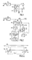
- the data clock pulse generator shown in Figure 1 simply comprises a data clock pulse source 101, a phase sensitive detector 102 and a storage capacitor 103.
- a data slicer 104 receives data pulses DP from an input terminal 105. After level correction and possibly re-shaping (by suitable known means not shown), the data pulses DP are applied to an output lead 106 for utilisation in further circuitry, the pulses DP being clocked into this further circuitry by means of clock pulses CK which are applied to a clock pulse lead 107 by the source 101.
- the data pulses DP and the clock pulses CK are also applied to the phase sensitive detector 102 which is responsive thereto to produce a control signal CS on a control lead 108, this control signal CS having a d.c. value in accordance with the relative phase of the data pulses DP and the clock pulses CK.
- This control signal CS is used to vary the voltage across the capacitor 103 to provide a control voltage for correcting the phase of the source 101 so as to bring the clock pulses CK into synchronism with the data pulses DP.
- the source 101 can comprise in known manner a voltage-controlled oscillator, together with means for limiting and squaring the output therefrom to form the clock pulses CK.
- the phase sensitive detector 102 takes the form shown in Figure 7, or in Figure 9, as will be described.
- the data clock pulse generator shown in Figure 2 is more elaborate than that shown in Figure 1 and has a specific application in a data pulse receiver arrangement for the aforesaid BBC/IBA Teletext television transmission system.
- This latter data clock pulse generator also comprises a data clock pulse source 201, a phase sensitive detector 202 and a storage capacitor 203, and a data slicer 204 receives data pulses DP from an input terminal 205 and feeds them to an output lead 206 for utilisation.
- clock pulses CK are produced on a clock pulse lead 207, and a control signal CS is produced on a control lead 208.
- a limiter 209 for limiting (and squaring) the output from the source 201.
- the source 201 comprises a crystal-controlled oscillator 210 and a phase shifter 211.
- the oscillator 210 produces a highly stable alternating signal at the clock frequency and the phase shifter211 is responsive in accordance with the d.c. value of the control signal CS to bring the oscillator output into phase synchronism with the data pulses DP.
- the phase shifter 211 can take any suitable known form, but preferably takes the form shown in our co-pending United Kingdom Patent Application No. 8039875 (PHB 32743).
- the phase sensitive detector 202 again takes the form shown in Figure 7 or in Figure 9, as will be described.
- the data clock pulse generator of Figure 2 additionally comprises a re-setting circuit 212, a timing circuit 213 and a voltage-to-current converter circuit 214.
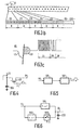
- Figure 3a shows a waveform diagram which represents a Teletext television video signal for one television line which occurs in a field-blanking interval and which includes coded pulse data.
- the line synchronising pulse for the television line concerned is represented at LS1
- the line synchronising pulse for the next television line is represented at LS2.
- the colour burst on the television line concerned and that on the next television line are represented at CB'1 and CB2, respectively.
- the period of one television line i.e. the period between the leading edges of successive line synchronising pulses
- is 64 ps as indicated. Further assuming the.
- the television line shown would be line number 17 or 18 in an even field and line number 330 or 331 in an odd field.
- Such a television line is referred to as a television data line and can contain coded data pulses representing 360 binary bits which may be considered as 45 eight-bit.bytes. The position of the coded pulse data in the data line is indicated at CPD.
- the binary bit signalling rate is approximately 7 Mbit/s, and the binary bit signalling levels are defined between a black level BL and a peak white level WL.
- the binary '0' le,vel is the black level BL and the binary '1' level is the level L.
- Figure 3b shows a possible format for coded pulse data in a television data line.
- the binary bits representing the coded pulse data are divided up into eight-bit bytes 1, 2, ... 20 ...
- the first two bytes 1 and 2 comprise a sequence of clock run-in pulses which in the present example consist of a sequence of alternating bits 10101010/10101010.
- the third byte 3 comprises a framing or start code, e.g. 11100100, which a data pulse receiver arrangement has to identify before it will respond to accept message information which is contained in the remaining eight-bit bytes 4, 5 ... 20....
- Figure 3c shows in idealised form the first part of a video signal waveform VS for a television data line showing the sequence of clock run-in pulses CL and the sequence of pulses which comprise the frame code FR.
- the first few coded data pulses which represent alpha-numeric characters or other message information are shown at DP.
- the line synchronising pulse is represented at LS and the colour burst at CB.
- the resetting circuit 212 is so organised in relation to the above coded data pulse transmission format that in each television data line it is operated by the line flyback pulse FL to connect a reference voltage RV across the capacitor 203 during the line blanking interval.
- This reference voltage RV sets the voltage across the capacitor 203 to a value corresponding to the middle of the phase range afforded by the phase shifter 211.
- the timing circuit 213 supplies to the voltage-to-current converter circuit 214 a timing pulse T which causes this circuit 214 to substantially increase (e.g.
- the circuit 214 double) its current output from a normal rate in response to the control signal CS (which it receives as a voltage) so that within this relatively short clock run-in period the control voltage across the capacitor 203 as produced by the current output of the circuit 214 can assume a mean value corresponding to the mean phase of the clock run-in pulses. For the remainder of the television data line, the circuit 214 operates to produce its current output at the normal, lower rate to provide a more stable control voltage about this mean value.
- the re-setting circuit 212 can take the form shown in Figure 4, wherein it simply comprises a field-effect transistor 401 which is arranged as an electronic switch to connect the reference voltage RV across the capacitor 203 during the application of the flyback pulse FL to its gate electrode.
- the timing circuit 213 can take the form shown in Figure 5, wherein it comprises a line synchronising pulse separator 501 and a pulse generator 502.
- the synchronising pulse separator 501 detects the line sync. pulses LS in the video signal VS to trigger the pulse generator 502 which is responsive to produce the timing pulse T by which the circuit 214 is operated.
- the pulse generator 502 includes a trigger delay such that the timing pulse T occurs at the beginning of the sequence of clock pulses CL and lasts for substantially the duration thereof.
- the voltage-to-current converter circuit 214 can take the form shown in Figure 6, wherein it comprises two converting elements 601 and 602 connected in parallel, with an electronic switch 603 (suitably comprised by a field-effect transistor in similar fashion to the transistor 401 in Figure 4) connected in series with the element 602.
- the control signal (voltage) CS is applied to both the elements 601 and 602 which thus both effect voltage-to-current conversion to feed current to the capacitor 203.
- the switch 603 is open, only the element 601 is operative to feed current to the capacitor 203.
- the elements 601 and 602 are incorporated in the current source circuit of Figure 11, as will be described.
- the phase sensitive detector shown in Figure 7 comprises two D-type flip-flops 701 and 702, two exclusive OR-gates 703 and 704, and a current source circuit 705.
- Each of the flip-flops 701 and 702 has a data input D, a clock input CK and a logic output Q (the other logic output Q is not shown).
- the data pulses DP are applied to the D-input of flip-flop 701, and the Q-output of flip-flop 701 is connected to the D-input of flip-flop 702.
- the clock pulses CK these are applied directly to the CK-input of flip-flop 701, and after inversion by an invertor 706 to the CK-input of flip-flop 702.
- the Q-output of flip-flop 701 is connected to a first input of each of the exclusive OR-gates 703 and 704.
- the Q-output of flip-flop 702 is connected to a second input of the exclusive OR-gate 703, and a second input of the exclusive OR-gate 704 is connected to receive the data pulses DP.
- the outputs of the exclusive OR-gates 703 and 704 are connected respectively to two current sources 707 and 708 in the circuit 705. There is also shown in Figure 7 the capacitor 203 across which the control signal voltage CS is produced.
- the pulse sequence D2 at the Q-output of the flip-flop 702, in response to the pulse sequence D1 at its D-input, is similarly delayed by one half a clock pulse period relative to the pulse sequence D1.
- This half a clock pulse period phase relationship between the pulse sequence D1 and the pulse sequence D2 remains constant irrespective of any shift in the relative phase of the data pulses DP and the clock pulses CK.
- variable phase relationship of the data pulses DP with respect to the pulse sequences D1 and D2 does affect the production of the outputs of the exclusive OR-gates 703 and 704, as will now be considered.
- the clock pulses CK are later (L) in phase than the data pulse DP, the latter have the rising edge 804 occurring somewhere along the shaded portion 805, as indicated by 804'.
- the clock pulses CK are earlier (E) in phase than the data pulses DP, the latter have the rising edge 804 occurring somewhere along the shaded portion 806, as indicated by 804".
- 704(C), 7-04(L) and 704(E)) varies from a duration of one half a clock pulse period when the phase relation is correct, to up to a full clock pulse period when the phase relation is late, and down to zero duration when the phase relation is early.
- the output from the exclusive OR-gate 703 controls the current source 707 to drive current into (charge) the capacitor 203 and the output from the exclusive OR-gate 704 controls the current source 708 to extract current from (discharge) the capacitor 203.
- the output of the gate 703 can be considered to be in anti-phase with the output of the gate 704, so that the resultant gate output for the above three phase situations can be represented by the resultant waveform diagrams 807 to 809.
- the charge on the capacitor 203 and hence the value of the control signal voltage CS is therefore altered proportionately as shown graphically at 810 to bring the clock pulses CK into synchronism with the data pulse DP.
- control signal voltage CS is directly proportional to the phase error in the desired phase relationship between the data pulses DP and the clock pulses CK, so that the required phase correction of the clock pulses CK can occur quickly to lock the phase into the desired relationship. Also, the value of the control signal voltage CS does not oscillate about the correct value for the desired phase relationship, but can instead hold at that correct value, because of the possible resultant "zero" output from the exclusive OR-gates 703 and 704 when the desired phase relationship obtains.
- the phase sensitive detector shown in Figure 9 comprises four D-type flip-flops 901 to 904, two exclusive OR-gates 905 and 906, and a current source circuit 907.
- Each of the flip-flops 901 to 904 has a data input D, a clock input CK and a logic output Q (the other logic output Q is not used).
- the data pulses DP are applied to the D-inputs of flip-flops 901 and 903, the Q-output of flip-flop 901 is connected to the D-input of flip-flop 902, and the Q-output of flip-flop 903 is connected to the D-input of flip-flop 904.
- clock pulses CK these are applied directly to the CK-inputs of flip-flops 901 and 904 and, after inversion by an inverter 910, to the CK-inputs of flip-flops 902 and 903.
- the Q-outputs of flip-flops 901 and 904 are connected to respective inputs of the exclusive OR-gate 906 and the Q-outputs of flip-flops 902 and 903 are connected to respective inputs of the exclusive OR-gate 905.
- the outputs of the gates 905 and 906 are connected respectively to two current sources 908 and 909 in the circuit 907.
- Figure 9 the capacitor 203 across which the control signal voltage CS is produced.
- the pulse sequence D2 at the Q-output of the flip-flop 902, in response to the pulse sequence D1 at its D-input, is similarly delayed by one-half a clock pulse period relative to the pulse sequence D1.
- This half a clock pulse period phase relationship between the pulse sequence D1 and the pulse sequence D2 remains constant irrespective of any shift in the relative phase of the data pulses DP and the clock pulses CK which varies the relative phase of the data pulses DP and the pulse sequence D1.
- the pulse sequence D3 will not start until its rising edge E1, when the rising edge RE2 of the inverted clock pulses CK occurs. If the pulse sequence D3 occurs early at L1, then the pulse sequence D4, as produced by the flip-flop 904, also occurs early at the rising edge L2 when the next rising edge of the clock pulses CK occurs, whereas if the pulse sequence D3 occurs late at E1, then the pulse sequence D4 also occurs late at the rising edge E2 when the next again rising edge of the clock pulses CK occurs.
- the current source circuit 705 in Figure 7 and 907 in Figure 9, can take the form shown in Figure 11, wherein it comprises two transistor pairs 1901/1902 and 1903/1904 of opposite conductivity type, both pairs being connected as current mirrors.
- the transistors 1902 and 1904 are connected in push-pull ⁇ with their collectors connected together and to the capacitor 203.
- the collectors of the other two transistors 1901 and 1903 are fed, respectively, with voltage pulses 1905 and 1906 which constitute the outputs from the exclusive OR-gates 703/905 and 704/906 ( Figures 7 and 9).
- An inverter 1907 inverts the pulses 1905 to form pulses 1905'.
- Two resistors 1908 and 1909 determine the current magnitude that flows in the transistors .1901 and 1903 in response to the voltage pulses 1905 and 1906.
- the resultant push-pull current in the transistors 1902 and 1904 adjusts the charge on the capacitor 203.
- a second current source circuit which is fed with the voltage pulses 1905 and 1906.
- the output at the collectors of the push-pull transistor pair in this second current source circuit is connected to the capacitor 203 via a field-effect transistor 1911 which functions as a switch in response to the timing pulse T, so that the capacitor 203 receives current from this second current source circuit only for the duration of this timing pulse T.
- the current due to the second current source can be proportionally different to that due to the first current source by suitable selection of the values of the resistors such as 1908 and 1909 in the second current source.
Landscapes
- Engineering & Computer Science (AREA)
- Power Engineering (AREA)
- Computer Networks & Wireless Communication (AREA)
- Signal Processing (AREA)
- Stabilization Of Oscillater, Synchronisation, Frequency Synthesizers (AREA)
Claims (7)
Applications Claiming Priority (4)
| Application Number | Priority Date | Filing Date | Title |
|---|---|---|---|
| GB8039874 | 1980-12-12 | ||
| GB8039874A GB2089601A (en) | 1980-12-12 | 1980-12-12 | Phase Sensitive Detector |
| GB8039873 | 1980-12-12 | ||
| GB8039873A GB2089600A (en) | 1980-12-12 | 1980-12-12 | Phase Sensitive Detector |
Publications (2)
| Publication Number | Publication Date |
|---|---|
| EP0054322A1 EP0054322A1 (fr) | 1982-06-23 |
| EP0054322B1 true EP0054322B1 (fr) | 1985-07-03 |
Family
ID=26277826
Family Applications (1)
| Application Number | Title | Priority Date | Filing Date |
|---|---|---|---|
| EP81201294A Expired EP0054322B1 (fr) | 1980-12-12 | 1981-11-23 | Détecteur sensible à la phase |
Country Status (3)
| Country | Link |
|---|---|
| US (1) | US4422176A (fr) |
| EP (1) | EP0054322B1 (fr) |
| DE (1) | DE3171263D1 (fr) |
Families Citing this family (57)
| Publication number | Priority date | Publication date | Assignee | Title |
|---|---|---|---|---|
| US4400667A (en) * | 1981-01-12 | 1983-08-23 | Sangamo Weston, Inc. | Phase tolerant bit synchronizer for digital signals |
| SE439083B (sv) * | 1981-11-30 | 1985-05-28 | Ellemtel Utvecklings Ab | Sett att bringa en oscillator i fas med en inkommande signal jemte anordning for genomforandet av settet |
| US4519086A (en) * | 1982-06-16 | 1985-05-21 | Western Digital Corporation | MOS Phase lock loop synchronization circuit |
| GB2124840A (en) * | 1982-07-02 | 1984-02-22 | Philips Electronic Associated | Data demodulator for digital signals |
| JPS5977633A (ja) * | 1982-10-26 | 1984-05-04 | Nippon Gakki Seizo Kk | デイスク再生装置におけるクロツク再生回路 |
| NL8401629A (nl) * | 1984-05-22 | 1985-12-16 | Philips Nv | Elektrische schakeling met een faseregelkring. |
| US4626913A (en) * | 1984-06-26 | 1986-12-02 | Rca Corporation | Chroma burst derived clock regenerator for teletext decoder |
| FR2569070B1 (fr) * | 1984-08-10 | 1991-04-19 | Milon Jean | Procede et dispositif d'acquisition rapide du rythme et de la phase d'un signal numerique |
| US4668918A (en) * | 1985-02-01 | 1987-05-26 | Advanced Micro Devices, Inc. | Low order charge-pump filter |
| US4698600A (en) * | 1985-02-04 | 1987-10-06 | International Business Machines Corporation | Clock phase discriminator |
| JPS61191121A (ja) * | 1985-02-20 | 1986-08-25 | Hitachi Ltd | 発振装置 |
| JPH0732391B2 (ja) * | 1985-05-28 | 1995-04-10 | 日本電気株式会社 | クロック同期回路 |
| NL8501887A (nl) * | 1985-07-01 | 1987-02-02 | Oce Nederland Bv | Fasedetector. |
| US4686677A (en) * | 1985-08-02 | 1987-08-11 | Unisys Corporation | Apparatus and method for detecting time-related faults |
| US4663769A (en) * | 1985-10-02 | 1987-05-05 | Motorola, Inc. | Clock acquisition indicator circuit for NRZ data |
| US4849704A (en) * | 1987-04-15 | 1989-07-18 | Westinghouse Electric Corp. | Duty cycle independent phase detector |
| US4811317A (en) * | 1987-06-25 | 1989-03-07 | Eastman Kodak Company | Clock resynchronization after a track jump |
| JPH0770168B2 (ja) * | 1987-08-17 | 1995-07-31 | 日本電気株式会社 | 磁気ディスク装置用pll回路 |
| US4884020A (en) * | 1988-07-22 | 1989-11-28 | Orion Instruments, Inc. | Phase detection system |
| JP2567479B2 (ja) * | 1988-10-17 | 1996-12-25 | 富士写真フイルム株式会社 | バーコードプリント装置 |
| KR920003598B1 (ko) * | 1988-12-22 | 1992-05-04 | 재단법인 한국전자통신 연구소 | Nrz비트 동기방식의 주파수 및 위상검출회로 |
| ATE103431T1 (de) * | 1989-07-18 | 1994-04-15 | Siemens Ag | Digitaler phasendetektor. |
| IT1231650B (it) * | 1989-07-21 | 1991-12-18 | Selenia Ind Elettroniche | Circuito per la ricostruzione del clock da un messaggio da utilizzare in sistemi di trasmissione dati |
| US5027085A (en) * | 1989-10-03 | 1991-06-25 | Analog Devices, Inc. | Phase detector for phase-locked loop clock recovery system |
| JPH0779363B2 (ja) * | 1990-06-29 | 1995-08-23 | 三菱電機株式会社 | 遅延検波回路 |
| US5170297A (en) * | 1990-07-13 | 1992-12-08 | Standard Microsystems Corporation | Current averaging data separator |
| KR930007716B1 (ko) * | 1990-07-20 | 1993-08-18 | 재단법인 한국전자통신연구소 | 비트 동기를 위한 디지틀 위상 검출기 |
| US5132990A (en) * | 1990-11-05 | 1992-07-21 | Ncr Corporation | High speed data synchronizer |
| US5159279A (en) * | 1990-11-27 | 1992-10-27 | Dsc Communications Corporation | Apparatus and method for detecting out-of-lock condition in a phase lock loop |
| ATE150240T1 (de) * | 1990-12-18 | 1997-03-15 | Alcatel Bell Nv | Synchronisationsschaltung |
| GB2251142B (en) * | 1990-12-22 | 1994-11-02 | Stc Plc | Signal detection apparatus |
| FR2673344B1 (fr) * | 1991-02-22 | 1993-05-28 | Telecommunications Sa | Comparateur de phase/frequence pour circuit de recuperation de rythme. |
| KR930007652B1 (ko) * | 1991-07-19 | 1993-08-14 | 한국전기 통신공사 | Cmi데이터 비트동기를 위한 위상검출기와 연동되어 동작하는 cmi/nrz복호기 |
| US5357216A (en) * | 1993-01-13 | 1994-10-18 | National Semiconductor Corporation | Current sourcing and sinking circuit for driving a VCO charge pump |
| US5506874A (en) * | 1993-11-01 | 1996-04-09 | Texas Instruments Incorporated | Phase detector and method |
| KR960002463B1 (ko) * | 1993-12-11 | 1996-02-17 | 한국전기통신공사 | 고속데이타 전송에서의 디지틀 데이타 리타이밍 장치 |
| US5640523A (en) * | 1994-09-02 | 1997-06-17 | Cypress Semiconductor Corporation | Method and apparatus for a pulsed tri-state phase detector for reduced jitter clock recovery |
| EP0741931A1 (fr) * | 1994-09-28 | 1996-11-13 | Koninklijke Philips Electronics N.V. | Boucle a phase asservie, comparateur de phase utile dans cette boucle et dispositif reproducteur comprenant celle-ci |
| US5473283A (en) * | 1994-11-07 | 1995-12-05 | National Semiconductor Corporation | Cascode switched charge pump circuit |
| KR970003097B1 (ko) * | 1994-12-02 | 1997-03-14 | 양승택 | 다단 제어구조를 갖는 고속 비트동기 장치 |
| DE4443417C1 (de) * | 1994-12-06 | 1996-02-22 | Siemens Ag | Phasendetektorschaltung |
| US5625360A (en) * | 1995-09-05 | 1997-04-29 | Motorola, Inc. | Current source for reducing noise glitches generated in a digital to analog converter and method therefor |
| US5770976A (en) * | 1996-12-11 | 1998-06-23 | Lucent Technologies Inc. | Local clock duty cycle independent phase detector and method of operation thereof |
| US6316966B1 (en) | 1999-07-16 | 2001-11-13 | Conexant Systems, Inc. | Apparatus and method for servo-controlled self-centering phase detector |
| DE19948690C2 (de) | 1999-09-30 | 2002-05-23 | Infineon Technologies Ag | Phasendetektor |
| GB2399264B (en) * | 2000-12-06 | 2005-02-09 | Fujitsu Ltd | Processing high-speed digital signals |
| DE10164837B4 (de) * | 2000-12-06 | 2006-04-27 | Fujitsu Ltd., Kawasaki | Verarbeitung von digitalen Hochgeschwindigkeitssignalen |
| US7061292B2 (en) * | 2001-11-09 | 2006-06-13 | The Regents Of The University Of Colorado | Adaptive voltage regulator for powered digital devices |
| US20030099307A1 (en) * | 2001-11-13 | 2003-05-29 | Narad Networks, Inc. | Differential slicer circuit for data communication |
| US20030091124A1 (en) * | 2001-11-13 | 2003-05-15 | Narad Networks, Inc. | Slicer circuit with ping pong scheme for data communication |
| RU2231915C2 (ru) * | 2002-04-16 | 2004-06-27 | Федеральное государственное унитарное предприятие "Конструкторское бюро "Луч" | Дифференциальный фазовый дискриминатор символьной синхронизации (его варианты) |
| JP4095367B2 (ja) * | 2002-07-23 | 2008-06-04 | 株式会社東芝 | 半導体集積回路装置 |
| US20040153681A1 (en) * | 2002-11-12 | 2004-08-05 | Broadcom Corporation | Phase detector for extended linear response and high-speed data regeneration |
| US7372928B1 (en) | 2002-11-15 | 2008-05-13 | Cypress Semiconductor Corporation | Method and system of cycle slip framing in a deserializer |
| JP3999168B2 (ja) * | 2003-07-04 | 2007-10-31 | シャープ株式会社 | キャリア検出回路およびそれを用いる赤外線通信装置 |
| US7605667B2 (en) * | 2007-04-26 | 2009-10-20 | Mediatek Inc. | Frequency synthesizer with a harmonic locked phase/frequency detector |
| US9647671B2 (en) | 2015-01-22 | 2017-05-09 | Wright State University | High performance phase frequency detectors |
Family Cites Families (8)
| Publication number | Priority date | Publication date | Assignee | Title |
|---|---|---|---|---|
| US3470488A (en) * | 1967-10-26 | 1969-09-30 | Int Standard Electric Corp | Automatic frequency acquisition circuit for a phase locked loop type of synchronizing system |
| US4010323A (en) * | 1975-10-29 | 1977-03-01 | Bell Telephone Laboratories, Incorporated | Digital timing recovery |
| US4128811A (en) * | 1977-07-05 | 1978-12-05 | General Electric Company | Frequency indicating circuit |
| US4151485A (en) * | 1977-11-21 | 1979-04-24 | Rockwell International Corporation | Digital clock recovery circuit |
| JPS5853809B2 (ja) * | 1977-12-20 | 1983-12-01 | 日本電気株式会社 | クロツクパルス再生回路 |
| JPS54124612A (en) * | 1978-03-22 | 1979-09-27 | Nippon Telegr & Teleph Corp <Ntt> | Receiving data detector circuit in data transmission |
| US4222009A (en) * | 1978-11-02 | 1980-09-09 | Sperry Corporation | Phase lock loop preconditioning circuit |
| US4237423A (en) * | 1978-12-08 | 1980-12-02 | Rca Corporation | Digital phase detector |
-
1981
- 1981-11-23 DE DE8181201294T patent/DE3171263D1/de not_active Expired
- 1981-11-23 EP EP81201294A patent/EP0054322B1/fr not_active Expired
- 1981-11-27 US US06/325,480 patent/US4422176A/en not_active Expired - Fee Related
Also Published As
| Publication number | Publication date |
|---|---|
| EP0054322A1 (fr) | 1982-06-23 |
| US4422176A (en) | 1983-12-20 |
| DE3171263D1 (en) | 1985-08-08 |
Similar Documents
| Publication | Publication Date | Title |
|---|---|---|
| EP0054322B1 (fr) | Détecteur sensible à la phase | |
| US4625320A (en) | Automatic bias circuit | |
| US4371974A (en) | NRZ Data phase detector | |
| US4358790A (en) | Electrical data pulse slicing | |
| JPS5825773A (ja) | 同期回路 | |
| EP0445806B1 (fr) | Circuit d'extraction d'un signal de synchronisation de bit utilisant la synchronisation de trâme | |
| US4431969A (en) | Clock pulse phase shifter | |
| US4301417A (en) | Quadriphase differential demodulator | |
| EP0056649B1 (fr) | Récepteur à signaux numériques | |
| US5778010A (en) | Method and device for correcting packet data error and packet receiver | |
| GB2089600A (en) | Phase Sensitive Detector | |
| GB2089601A (en) | Phase Sensitive Detector | |
| US3991270A (en) | Circuit arrangement for line synchronization in a television receiver | |
| US5243630A (en) | Method of and arrangement for generating a clock signal from a biphase modulated digital signal | |
| US4198659A (en) | Vertical synchronizing signal detector for television video signal reception | |
| US4362997A (en) | Quadriphase differential demodulator | |
| US4415933A (en) | Carrier wave recovery circuit | |
| US3968446A (en) | Frequency and phase control system | |
| US3080452A (en) | Synchronous communication systems | |
| US5784121A (en) | Vertical synchronisation signal detector | |
| US4051537A (en) | Facsimile receiving apparatus | |
| JP3069830B2 (ja) | バイポーラ/ユニポーラ変換回路 | |
| EP0487072A2 (fr) | Générateur de signal de déflection verticale | |
| GB2089599A (en) | Data Clock Pulse Generator | |
| JP3312089B2 (ja) | 位相基準検出装置 |
Legal Events
| Date | Code | Title | Description |
|---|---|---|---|
| PUAI | Public reference made under article 153(3) epc to a published international application that has entered the european phase |
Free format text: ORIGINAL CODE: 0009012 |
|
| AK | Designated contracting states |
Designated state(s): DE FR GB IT |
|
| RAP1 | Party data changed (applicant data changed or rights of an application transferred) |
Owner name: N.V. PHILIPS' GLOEILAMPENFABRIEKEN Owner name: PHILIPS ELECTRONIC AND ASSOCIATED INDUSTRIES LIMIT |
|
| 17P | Request for examination filed |
Effective date: 19820922 |
|
| ITF | It: translation for a ep patent filed | ||
| GRAA | (expected) grant |
Free format text: ORIGINAL CODE: 0009210 |
|
| AK | Designated contracting states |
Designated state(s): DE FR GB IT |
|
| REF | Corresponds to: |
Ref document number: 3171263 Country of ref document: DE Date of ref document: 19850808 |
|
| ET | Fr: translation filed | ||
| PLBE | No opposition filed within time limit |
Free format text: ORIGINAL CODE: 0009261 |
|
| STAA | Information on the status of an ep patent application or granted ep patent |
Free format text: STATUS: NO OPPOSITION FILED WITHIN TIME LIMIT |
|
| 26N | No opposition filed | ||
| ITTA | It: last paid annual fee | ||
| PGFP | Annual fee paid to national office [announced via postgrant information from national office to epo] |
Ref country code: GB Payment date: 19941031 Year of fee payment: 14 |
|
| PGFP | Annual fee paid to national office [announced via postgrant information from national office to epo] |
Ref country code: FR Payment date: 19941125 Year of fee payment: 14 |
|
| PGFP | Annual fee paid to national office [announced via postgrant information from national office to epo] |
Ref country code: DE Payment date: 19950124 Year of fee payment: 14 |
|
| ITPR | It: changes in ownership of a european patent |
Owner name: CAMBIO RAGIONE SOCIALE;PHILIPS ELECTRONICS N.V. |
|
| REG | Reference to a national code |
Ref country code: FR Ref legal event code: CD |
|
| PG25 | Lapsed in a contracting state [announced via postgrant information from national office to epo] |
Ref country code: GB Effective date: 19951123 |
|
| GBPC | Gb: european patent ceased through non-payment of renewal fee |
Effective date: 19951123 |
|
| PG25 | Lapsed in a contracting state [announced via postgrant information from national office to epo] |
Ref country code: FR Effective date: 19960731 |
|
| PG25 | Lapsed in a contracting state [announced via postgrant information from national office to epo] |
Ref country code: DE Effective date: 19960801 |
|
| REG | Reference to a national code |
Ref country code: FR Ref legal event code: ST |