EP0055592A2 - Dispositif de prise de vue à l'état solide - Google Patents
Dispositif de prise de vue à l'état solide Download PDFInfo
- Publication number
- EP0055592A2 EP0055592A2 EP81306055A EP81306055A EP0055592A2 EP 0055592 A2 EP0055592 A2 EP 0055592A2 EP 81306055 A EP81306055 A EP 81306055A EP 81306055 A EP81306055 A EP 81306055A EP 0055592 A2 EP0055592 A2 EP 0055592A2
- Authority
- EP
- European Patent Office
- Prior art keywords
- mosts
- vertical
- gate lines
- field switching
- vertical gate
- Prior art date
- Legal status (The legal status is an assumption and is not a legal conclusion. Google has not performed a legal analysis and makes no representation as to the accuracy of the status listed.)
- Granted
Links
Images


Classifications
-
- H—ELECTRICITY
- H04—ELECTRIC COMMUNICATION TECHNIQUE
- H04N—PICTORIAL COMMUNICATION, e.g. TELEVISION
- H04N25/00—Circuitry of solid-state image sensors [SSIS]; Control thereof
- H04N25/70—SSIS architectures; Circuits associated therewith
- H04N25/76—Addressed sensors, e.g. MOS or CMOS sensors
- H04N25/767—Horizontal readout lines, multiplexers or registers
-
- H—ELECTRICITY
- H04—ELECTRIC COMMUNICATION TECHNIQUE
- H04N—PICTORIAL COMMUNICATION, e.g. TELEVISION
- H04N25/00—Circuitry of solid-state image sensors [SSIS]; Control thereof
- H04N25/70—SSIS architectures; Circuits associated therewith
- H04N25/76—Addressed sensors, e.g. MOS or CMOS sensors
Definitions
- the present invention relates to a solid-state imaging device.
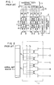
- Fig. 1 shows a schematic diagram of a conventional solid-state area image sensor. It comprises a number of photodiodes 1 as photo-electric conversion elements arranged in a matrix form, vertical switching insulated gate field effect transistors (MOSTs) 2 and horizontal switching MOSTs 3 for reading out desired signals stored in the photodiodes 1, and vertical and horizontal shift registers 4 and 5 for sequentially switching the switches 2 and 3.
- MOSTs vertical switching insulated gate field effect transistors
- a part including the photodiode 1 and the vertical switching MOST 2 for each picture element forms a photosensing part.
- Numeral 6 denotes vertical gate lines
- numeral 7 denotes vertical signal output lines
- numerals 8, 16, 17, 18 and 19 denote horizontal gate lines
- numerals 9 and 10 denote horizontal signal output lines which are connected to signal output terminals.
- the vertical and horizontal switching MOSTs 2 and 3 have their gate voltages controlled by the shift registers 4 and 5 to carry out the switching operations.
- a signal readout scheme called an interlace mode operation has been used.
- the vertical gate lines 6 are designated by A, B, ... from the bottom to the top in Fig. 1, signals on the lines A+B, C+D, E+F, ... are read in a first field period, and signals on the lines A, B+C, D+E, ... are read in a second field period.
- numeral 11 denotes an interlace circuit which allocates the output pulses or vertical scan pulses of the vertical shift register 4 to the vertical gate lines of the respective fields F1 and F 2 .
- Fig. 2 shows a conventional interlace circuit.
- the pulses are applied to the vertical gate lines in the sequence of A+B, C+D, E+F, ... in the first field (F1) period, to read the signals.
- the pulses are applied in the sequence of A, B+C, D+E, ... to read the signals. In this manner, the signals are read in the interlace mode.
- a timing of the pulses of the circuit of Fig. 2 is shown in Fig. 3.
- a D.C. level of a video signal varies depending on a field so that a flicker appears on a reproduced picture image.
- a mechanism of the generation of the flicker is explained with reference to Figs. 4 and 5.
- Fig. 4 shows some picture elements in the photosensing part shown in Fig. 1. Each picture element comprises a photodiode 43 and a vertical switching MOST 44.
- Numerals 30, 31 and 32 denote vertical gate lines
- numerals 41 and 42 denote coupling capacitances
- numeral 43 denotes photodiodes
- numeral 44 denotes vertical switching MOSTs
- numerals 46 and 47 denote vertical signal output lines to which video bias voltages V v are externally applied.
- V SC potential of the photodiode 43
- V SC is substantially equal to the video bias V v so that a reset state is attained, but when the potential of C is low, V SC falls because of the coupling capacitance which is parasitically present between the vertical gate line and the photodiode.
- the coupling capacitance varies with the field.
- Fig. 5 shows a variation thereof and a pulse timing.
- the vertical gate lines C (31) and D (32) are selected at the same timing, and in the second field in which the second field switching pulse F 2 is of high level, the vertical gate lines B (30) and C (31) are simultaneously selected.
- V SC when the vertical gate line C changes from the high level to the low level (at the timing shown by 53 and 55) in the F 1 field, only C PCl (41) acts as the coupling capacitance because the vertical gate line B remains at the low level.
- the drop ⁇ V Sl of V SC is small as shown by 51 in Fig. 5.
- a buffer circuit is provided between the vertical gate lines and the interlace circuit to first turn off the vertical gate line associated with the picture element which has a coupling capacitance with only one of the two simultaneously selected vertical gate lines, and to thereafter turn off the vertical gate line associated with the picture element which has coupling capacitances with both of the simultaneously selected vertical gate lines.
- Fig. 6 which shows a schematic circuit diagram of a solid-state imaging device according to one embodiment of the present invention
- numeral 101 denotes a novel buffer circuit
- Fig. 7 shows an example of the buffer circuit together with a vertical shift register and an interlace-circuit
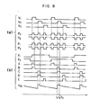
- Fig. 8 shows a timing chart for explaining the operation of the buffer circuit of Fig. 7.
- numeral 121 denotes a part of the vertical shift register 4.
- Numerals 122 to 131 denote field switching MOSTs for interlace operation, four field switching MOSTs being provided for each stage of the vertical shift register,
- numerals 132 and 133 denote first and second field pulse lines for supplying first and second field switching pulses F l and F 2 , and these elements forms an interlace circuit 11.
- Numerals 161 to 166 denote vertical gate lines
- numerals 147 and 148 denote first and second drive pulse lines for supplying first and second drive pulses P 1 and P 2 which are to be applied to the vertical gate lines and are synchronized with the vertical scan pulses V 1 to V 3 from the vertical shift register 121
- numerals 141 to 146 denote transfer MOSTs for sequentially selecting P 1 and P 2
- numeral 170 denotes bootstrap capacitances
- numerals 167 and 165 denote first and second reset lines for supplying first and second reset pulses P 3 and P 4 to fully turn off the voltages on the vertical gate lines
- numerals 151 to 156 denote reset MOSTs controlled by the reset pulses P 3 and P 4 .
- the first and second field pulses F 1 and F 2 select the corresponding field switching MOSTs (122 to 131). For example, when F 2 is ON (high level), the pairs of MOSTs 124, 125; 128, 129,; ... are selected. This corresponds to the selection of the pairs of vertical gate lines B, C; D, E; .... When F 1 is ON, the pairs of MOSTs 122, 123; 126, 127; 130, 131 are selected.
- the pulses P 1 and P 2 are turned ON (high level) when V 2 is ON (high level) and F 2 is ON, the corresponding gate lines 162 (B) and 163 (C) are turned ON (high level) (at time t 1 in Fig. 8).
- the bootstrap capacitances 170 as shown in Fig. 7, the potentials on the vertical gate lines are raised to the high levels of the pulses P 1 and P 2 independently of the threshold voltages of the transistors (142, 143).
- P 1 is turned OFF (low level) and P 3 is turned ON (high level) so that the vertical gate line 162 (B) is turned OFF (low level) (at time t 2 ).
- P 2 is turned OFF (low level) and P 4 is turned ON (high level) so that the line C is turned OFF (low level).
- the vertical gate line B can be turned OFF prior to the vertical gate line C.
- the pairs of D and E, ... which have been selected.
- the pairs A, B; C, D; ... are selected.
- the gate line A can be turned OFF prior to B, and the gate line C can be turned OFF prior to D.
- Fig. 8 further shows a drive pulse timing (a) of the buffer circuit shown in Fig. 7.
- the offset of timing at the transition to OFF is presented by switching the timings of the pulses P 1 , P 3 , P 2 , P 4 for each field.
- the buffer circuit is not limited to the particular circuit shown in Fig. 7.
- the drive pulse lines for P I and P 2 may be common.
- the timing is to be adjusted such that after V l , V 2 , ... (vertical register outputs) have been changed from ON to OFF, the reset pulses P 3 and P 4 are turned ON. In this manner, the outputs (A, B, ... ) as shown in (b) of Fig. 8 are produced.
- P 3 and P 4 may be common. In this case, the common pulses P3 and P4 is synchronized with one of P 1 and P 2 which is later turned OFF.
- An essential feature of the present invention resides in the solid-state imaging device operated in the simultaneous selection mode of two lines in which the gate line for the photodiode which has the coupling capacitance with only one of the two selected vertical gate lines is turned OFF first and the gate line for the photodiode which is encircled by the two selected vertical gate lines and has coupling capacitances therewith is turned OFF next so that the flicker which would otherwise be caused by the unbalance of the coupling capacitances among the fields is prevented and the high sensitivity solid-state imaging device which can produce a high quality of image under a low illumination is provided.
- the drive circuits and the pulse sequences are not limited to the illustrated examples.
Landscapes
- Engineering & Computer Science (AREA)
- Multimedia (AREA)
- Signal Processing (AREA)
- Transforming Light Signals Into Electric Signals (AREA)
- Color Television Image Signal Generators (AREA)
Applications Claiming Priority (2)
| Application Number | Priority Date | Filing Date | Title |
|---|---|---|---|
| JP55186391A JPS57109488A (en) | 1980-12-26 | 1980-12-26 | Solid color image pickup device |
| JP186391/80 | 1980-12-26 |
Publications (3)
| Publication Number | Publication Date |
|---|---|
| EP0055592A2 true EP0055592A2 (fr) | 1982-07-07 |
| EP0055592A3 EP0055592A3 (en) | 1983-09-07 |
| EP0055592B1 EP0055592B1 (fr) | 1985-10-02 |
Family
ID=16187569
Family Applications (1)
| Application Number | Title | Priority Date | Filing Date |
|---|---|---|---|
| EP81306055A Expired EP0055592B1 (fr) | 1980-12-26 | 1981-12-22 | Dispositif de prise de vue à l'état solide |
Country Status (4)
| Country | Link |
|---|---|
| US (1) | US4413283A (fr) |
| EP (1) | EP0055592B1 (fr) |
| JP (1) | JPS57109488A (fr) |
| DE (1) | DE3172559D1 (fr) |
Cited By (5)
| Publication number | Priority date | Publication date | Assignee | Title |
|---|---|---|---|---|
| GB2170374A (en) * | 1984-12-28 | 1986-07-30 | Canon Kk | Image sensing apparatus |
| GB2191059A (en) * | 1985-08-02 | 1987-12-02 | Trt Telecom Radio Electr | Electronic interlaced scanning, for a thermal camera |
| US4816910A (en) * | 1984-12-28 | 1989-03-28 | Canon Kabushiki Kaisha | Image sensing apparatus |
| WO1999059360A1 (fr) * | 1998-05-08 | 1999-11-18 | Telefonaktiebolaget Lm Ericsson (Publ) | Procede et conception relatifs a un systeme de radiocommunication |
| WO2001003418A1 (fr) * | 1999-07-05 | 2001-01-11 | Koninklijke Philips Electronics N.V. | Detecteur d'images |
Families Citing this family (12)
| Publication number | Priority date | Publication date | Assignee | Title |
|---|---|---|---|---|
| FR2504334B1 (fr) * | 1981-04-16 | 1985-10-18 | Thomson Csf | Dispositif d'analyse d'image en lignes successives, utilisant le transfert de charges electriques, composant une memoire de ligne, et camera de television comportant un tel dispositif |
| DE3138294A1 (de) * | 1981-09-25 | 1983-04-14 | Siemens AG, 1000 Berlin und 8000 München | Zweidimensionaler halbleiter-bildsensor mit steuerung oder regelung der integrationszeit |
| US4620222A (en) * | 1982-11-10 | 1986-10-28 | Matsushita Electric Industrial Co., Ltd. | Digital color TV camera |
| JPH0628450B2 (ja) * | 1983-01-28 | 1994-04-13 | 松下電器産業株式会社 | 固体撮像装置 |
| US4542409A (en) * | 1983-03-25 | 1985-09-17 | Fuji Photo Film Co., Ltd. | Single gate line interlace solid-state color imager |
| JPS59181884A (ja) * | 1983-03-31 | 1984-10-16 | Matsushita Electric Ind Co Ltd | カラ−カメラ装置 |
| JPS6055781A (ja) * | 1983-09-07 | 1985-04-01 | Nec Corp | 固体撮像素子 |
| US4905265A (en) * | 1985-12-11 | 1990-02-27 | General Imaging Corporation | X-ray imaging system and solid state detector therefor |
| JPH0695735B2 (ja) * | 1985-12-25 | 1994-11-24 | キヤノン株式会社 | 固体撮像装置 |
| US4804854A (en) * | 1987-02-16 | 1989-02-14 | Shimadzu Corporation | Low-noise arrayed sensor radiation image detecting system wherein each sensor connects to a buffer circuit |
| US5596200A (en) * | 1992-10-14 | 1997-01-21 | Primex | Low dose mammography system |
| JP5312758B2 (ja) * | 2007-06-13 | 2013-10-09 | 株式会社ジャパンディスプレイ | 表示装置 |
Family Cites Families (4)
| Publication number | Priority date | Publication date | Assignee | Title |
|---|---|---|---|---|
| JPS571958B2 (fr) * | 1974-04-25 | 1982-01-13 | ||
| JPS5853830B2 (ja) * | 1977-07-13 | 1983-12-01 | 株式会社日立製作所 | カラ−固体撮像装置 |
| JPS5511682A (en) * | 1978-07-12 | 1980-01-26 | Nec Corp | Color image pickup device |
| JPS56152382A (en) * | 1980-04-25 | 1981-11-25 | Hitachi Ltd | Solid image pickup element |
-
1980
- 1980-12-26 JP JP55186391A patent/JPS57109488A/ja active Granted
-
1981
- 1981-12-21 US US06/332,933 patent/US4413283A/en not_active Expired - Fee Related
- 1981-12-22 EP EP81306055A patent/EP0055592B1/fr not_active Expired
- 1981-12-22 DE DE8181306055T patent/DE3172559D1/de not_active Expired
Cited By (9)
| Publication number | Priority date | Publication date | Assignee | Title |
|---|---|---|---|---|
| GB2170374A (en) * | 1984-12-28 | 1986-07-30 | Canon Kk | Image sensing apparatus |
| DE3546141A1 (de) * | 1984-12-28 | 1986-08-14 | Canon K.K., Tokio/Tokyo | Bildlesegeraet |
| US4816910A (en) * | 1984-12-28 | 1989-03-28 | Canon Kabushiki Kaisha | Image sensing apparatus |
| GB2170675B (en) * | 1984-12-28 | 1989-12-13 | Canon Kk | Image sensing apparatus |
| DE3546809C2 (fr) * | 1984-12-28 | 1993-05-19 | Canon K.K., Tokio/Tokyo, Jp | |
| GB2191059A (en) * | 1985-08-02 | 1987-12-02 | Trt Telecom Radio Electr | Electronic interlaced scanning, for a thermal camera |
| WO1999059360A1 (fr) * | 1998-05-08 | 1999-11-18 | Telefonaktiebolaget Lm Ericsson (Publ) | Procede et conception relatifs a un systeme de radiocommunication |
| WO2001003418A1 (fr) * | 1999-07-05 | 2001-01-11 | Koninklijke Philips Electronics N.V. | Detecteur d'images |
| US6844898B1 (en) | 1999-07-05 | 2005-01-18 | Koninklijke Philips Electronics N.V. | Image detector |
Also Published As
| Publication number | Publication date |
|---|---|
| DE3172559D1 (en) | 1985-11-07 |
| US4413283A (en) | 1983-11-01 |
| JPH0345593B2 (fr) | 1991-07-11 |
| EP0055592B1 (fr) | 1985-10-02 |
| JPS57109488A (en) | 1982-07-07 |
| EP0055592A3 (en) | 1983-09-07 |
Similar Documents
| Publication | Publication Date | Title |
|---|---|---|
| US4413283A (en) | Solid-state imaging device | |
| US5146339A (en) | Photoelectric converting apparatus employing Darlington transistor readout | |
| US9129879B2 (en) | Solid state imaging device and camera system | |
| EP0168030B1 (fr) | Dispositif de lecture d'images du type contact et sa méthode de fonctionnement | |
| US5051831A (en) | Solid state image pickup apparatus for accumulating and reading out optical information using multi-phase scanning pulses | |
| JP2768686B2 (ja) | トランジスタ・イメージ・センサ・アレイとこれを用いて像を検出する方法並びに電圧信号を感知する装置および方法 | |
| KR100817801B1 (ko) | 고체 촬상 장치 및 카메라 시스템 | |
| JP2001128070A (ja) | 自己補償型相関二重サンプリング回路 | |
| US4189749A (en) | Solid state image sensing device | |
| EP0569202B1 (fr) | Capteur d'images à l'état solide avec obturateur électronique | |
| US4922138A (en) | Scan circuit using a plural bootstrap effect for forming scan pulses | |
| EP0653881A2 (fr) | Dispositif de prise de vues à l'état solide | |
| JPS6161586B2 (fr) | ||
| US5134489A (en) | X-Y addressable solid state imager for low noise operation | |
| JP3353921B2 (ja) | 固体撮像装置 | |
| US5883668A (en) | Solid-state image pickup apparatus | |
| EP0766455B1 (fr) | Méthode de commande d'un dispositif à transfert de charges | |
| JP2656475B2 (ja) | 固体撮像装置 | |
| EP0725535B1 (fr) | Dispositif de prise de vues à l'état solide et son procédé de mise en oeuvre | |
| US6784932B1 (en) | Hierarchical pixel readout multiplexer with switched capacitors for cancelling buffer offsets | |
| JP2776804B2 (ja) | 固体撮像装置 | |
| JP2598103B2 (ja) | 光電変換装置 | |
| KR20240105834A (ko) | 엑스선 디텍터 | |
| JP2511867B2 (ja) | 固体撮像装置 | |
| KR850000366B1 (ko) | 고체촬상소자 |
Legal Events
| Date | Code | Title | Description |
|---|---|---|---|
| PUAI | Public reference made under article 153(3) epc to a published international application that has entered the european phase |
Free format text: ORIGINAL CODE: 0009012 |
|
| AK | Designated contracting states |
Designated state(s): DE FR NL |
|
| PUAL | Search report despatched |
Free format text: ORIGINAL CODE: 0009013 |
|
| AK | Designated contracting states |
Designated state(s): DE FR NL |
|
| 17P | Request for examination filed |
Effective date: 19831209 |
|
| GRAA | (expected) grant |
Free format text: ORIGINAL CODE: 0009210 |
|
| AK | Designated contracting states |
Designated state(s): DE FR NL |
|
| REF | Corresponds to: |
Ref document number: 3172559 Country of ref document: DE Date of ref document: 19851107 |
|
| ET | Fr: translation filed | ||
| PLBE | No opposition filed within time limit |
Free format text: ORIGINAL CODE: 0009261 |
|
| STAA | Information on the status of an ep patent application or granted ep patent |
Free format text: STATUS: NO OPPOSITION FILED WITHIN TIME LIMIT |
|
| 26N | No opposition filed | ||
| PGFP | Annual fee paid to national office [announced via postgrant information from national office to epo] |
Ref country code: NL Payment date: 19871231 Year of fee payment: 7 |
|
| PG25 | Lapsed in a contracting state [announced via postgrant information from national office to epo] |
Ref country code: NL Effective date: 19890701 |
|
| NLV4 | Nl: lapsed or anulled due to non-payment of the annual fee | ||
| PGFP | Annual fee paid to national office [announced via postgrant information from national office to epo] |
Ref country code: FR Payment date: 19900922 Year of fee payment: 10 |
|
| PGFP | Annual fee paid to national office [announced via postgrant information from national office to epo] |
Ref country code: DE Payment date: 19901228 Year of fee payment: 10 |
|
| PG25 | Lapsed in a contracting state [announced via postgrant information from national office to epo] |
Ref country code: FR Effective date: 19920831 |
|
| PG25 | Lapsed in a contracting state [announced via postgrant information from national office to epo] |
Ref country code: DE Effective date: 19920901 |
|
| REG | Reference to a national code |
Ref country code: FR Ref legal event code: ST |