EP0056738A2 - Festkörper-Bildaufnahmevorrichtung mit Rauschunterdrückung - Google Patents
Festkörper-Bildaufnahmevorrichtung mit Rauschunterdrückung Download PDFInfo
- Publication number
- EP0056738A2 EP0056738A2 EP82300289A EP82300289A EP0056738A2 EP 0056738 A2 EP0056738 A2 EP 0056738A2 EP 82300289 A EP82300289 A EP 82300289A EP 82300289 A EP82300289 A EP 82300289A EP 0056738 A2 EP0056738 A2 EP 0056738A2
- Authority
- EP
- European Patent Office
- Prior art keywords
- output
- signal
- state imaging
- solid
- imaging apparatus
- Prior art date
- Legal status (The legal status is an assumption and is not a legal conclusion. Google has not performed a legal analysis and makes no representation as to the accuracy of the status listed.)
- Granted
Links
Images


Classifications
-
- H—ELECTRICITY
- H03—ELECTRONIC CIRCUITRY
- H03K—PULSE TECHNIQUE
- H03K17/00—Electronic switching or gating, i.e. not by contact-making and –breaking
-
- H—ELECTRICITY
- H04—ELECTRIC COMMUNICATION TECHNIQUE
- H04N—PICTORIAL COMMUNICATION, e.g. TELEVISION
- H04N25/00—Circuitry of solid-state image sensors [SSIS]; Control thereof
- H04N25/60—Noise processing, e.g. detecting, correcting, reducing or removing noise
- H04N25/62—Detection or reduction of noise due to excess charges produced by the exposure, e.g. smear, blooming, ghost image, crosstalk or leakage between pixels
- H04N25/628—Detection or reduction of noise due to excess charges produced by the exposure, e.g. smear, blooming, ghost image, crosstalk or leakage between pixels for reducing horizontal stripes caused by saturated regions of CMOS sensors
-
- H—ELECTRICITY
- H04—ELECTRIC COMMUNICATION TECHNIQUE
- H04N—PICTORIAL COMMUNICATION, e.g. TELEVISION
- H04N25/00—Circuitry of solid-state image sensors [SSIS]; Control thereof
- H04N25/60—Noise processing, e.g. detecting, correcting, reducing or removing noise
- H04N25/618—Noise processing, e.g. detecting, correcting, reducing or removing noise for random or high-frequency noise
-
- H—ELECTRICITY
- H04—ELECTRIC COMMUNICATION TECHNIQUE
- H04N—PICTORIAL COMMUNICATION, e.g. TELEVISION
- H04N25/00—Circuitry of solid-state image sensors [SSIS]; Control thereof
- H04N25/60—Noise processing, e.g. detecting, correcting, reducing or removing noise
- H04N25/67—Noise processing, e.g. detecting, correcting, reducing or removing noise applied to fixed-pattern noise, e.g. non-uniformity of response
Definitions
- This invention relates to a solid-state imaging apparatus in which photo signals are read out through MO S type field effect transistors from a large number of photosensors arrayed in two dimensions.
- a solid-state imaging apparatus wherein a plurality of photosensors such as photodiodes are arrayed in horizontal and vertical directions on a semiconductor substrate and wherein signal charges corresponding to the quantities of incident light as stored in the respective photosensors are sequentially read out through switches constructed of MOS type field effect transistors (hereinbelow, termed "MOS-FETs"), has the advantages that comparatively great charge signals can be handled and that the dark current is small. See for example EP 0022323.
- MOS-FETs MOS type field effect transistors
- the MOS type solid-state imaging apparatus involves the problem that noise which develops from the switches for controlling the readout of the signals of the photosensors, especially the switches for the. horizontal scanning, is delivered in superposition on the photo signals from the photosensors.
- the noise is classified into so-called ⁇ "fixed pattern noi.se" which appears as fixed vertical stripes on a reproduced picture, and "random noise” which appears as irregular fluctuations. Although the cause of the former noise has been cleared up, no effective method of reducing the latter noise has been found at present.
- a solid-state imaging apparatus wherein a plurality of photosensors are arrayed in horizontal and vertical directions on a semiconductor substrate, photo signal outputs from the photosensors are read out onto vertical signal lines through a first group of switches which are driven by vertical scanning pulses, and the photo signal outputs on the respective vertical signal lines are fetched onto an output line through a second group of switches which are driven by horizontal scanning pulses, is so constructed as to add the output from the output line and a signal with the output delayed by a period which is shorter than one horizontal scanning period by the time of one horizontal scanning pulse and to deliver the resulting signal as a video signal.
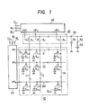
- FIG. 1 shows an example of a MOS type solid-state imaging apparatus to which this invention is applied.
- This solid-state imaging apparatus is constructed of a photosensitive portion 10, a vertical scanning circuit 20, a horizontal switching portion 30 and a horizontal scanning circuit 40.
- photodiodes D 11 - D are arrayed in two dimensions with n photodiodes being included in each row in the horizontal direction and m photodiodes being included 'in each column in the vertical direction.
- Signals of the photodiodes D 11 - D mn are read out onto vertical signal lines 11 - 1N through vertical switches S 11 - S mn which are MOS-FETs.
- the gates of the vertical switches S 11 - S mn are connected to horizontal signal lines 21 - 2M in such a manner that those of the vertical switches in an identical row are collectively connected to the corresponding horizontal signal line.
- the photodiodes D 11 - D mn , the vertical switches S 11 - S mn' the vertical signal lines 11 - 1N and the horizontal signal lines 21 - 2M constitute the photosensitive portion 10.
- the vertical switches S 11 - S mn have their respective rows controlled “on” and “off” by output pulses VP l - VP m from the vertical scanning circuit 20.
- This vertical scanning circuit 20 is constructed of, for example, a shift register which operates to shift a vertical input pulse CL 2 by the use of clocks ⁇ 3 and ⁇ 4 synchronous with the horizontal scanning.
- the group of horizontal switches 30 are constructed of horizontal switches S l - S n being MOS-FETs which serve to supply an output line 50 with the photo signals read out onto the vertical signal readout lines 11 - 1N. These switches are sequentially controlled “on” and “ off” by output pulses HP1 - HP n from the horizontal scanning circuit 40.
- This horizontal scanning circuit 40 is also constructed of, for example, a shift register which operates to shift a horizontal input pulse CL 1 with clocks ⁇ 1 and ⁇ 2 .
- An output line 50 is connected to a preamplifier not shown.
- the combined capacitance between the input capacitance of the preamplifier and the stray capacitance of the output line 50 is indicated by a capacitor 51.
- the input impedance of the preamplifier is indicated by a resistance element 52, and a power source by a part 53.
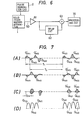
- the video signal is as illustrated in Figure 2.
- the vertical scanning pulse VP 1 has become “1" and has been impressed on the horizontal signal line 21
- signal charges Q s11 - Q sln corresponding to the quantities of incident light and stored in the photodiodes D 11 - D 1n of the first row appear on the vertical signal lines 11 - 1N, respectively.
- the horizontal-switches S 1 - S 1n have been sequentially turned “on” by the horizontal scanning pulses HP l - HP n
- photo signal outputs V 0 as shown in Figure 2 are read out onto the output line 50.
- the outputs V 0 in Figure 2 illustrate only photo signal components free from noise components, and their peak values represent the intensities of light.
- the photo signal V 0 is smoothed by passing it through a low-pass filter which has a cutoff frequency equal to half of the frequency of the horizontal scanning pulses.
- the video signal V s can be obtained.
- the noise components appear in superposition on the photo signal V .
- the fixed pattern noise appears as indicated at FP. in Figure 3. That is, in response to the voltage V Hj of the horizontal pulse HP j , current Fp j flows from the power source 53 so as to charge the gate - source path of the horizontal switch. The quantity of charges Q j to be stored at this time is determined by the gate capacitance of the horizontal switch, the stray capacitance of the vertical signal line and the capacitance 51 of the output circuit. When the horizontal pulse HP . has turned “off”, current flows so as to erase the charges Q j .
- the gate capacitance of the horizontal switch and the stray capacitance of the vertical signal line have different values in dependence on the horizontal position of the imaging apparatus.
- the noi.se components FP. are accordingly inherent in the horizontal direction, and they form vertical stripe patterns on a screen.
- the fixed pattern noise can therefore be erased by integrating the output signal of the output line 50 for a period (T ON + T ON ').
- the inventors of the present invention further analyzed the random noise. As a result, it has been found out that the random noise contains components having a vertical correlation. On the basis of this finding, we propose to effectively eliminate the random noise by exploiting the vertical correlation. Hereunder, the operating principle by which this is done will be described.
- the group of vertical switches S 11 - S mn and the group of horizontal switches S l - S n are considered as random noise sources, but noise from the former are very small. noisy.se from the group of horizontal switches are therefore considered, and the random noise circuit of this group of switches can be simulated as shown in Figure 4.
- R 1 - R n denote the "on" resistances of the horizontal switches S 1 - S n
- thermal noise generated therefrom is indicated by e 1 - e n
- C 1 - C n indicate the stray capacitances of the vertical signal lines connected to the respective horizontal switches.
- T denote the absolute temperature of the resistance R i and ⁇ f a frequency bandwidth
- random noise currents IA 1 and IA 2 as shown in Figure 5 flow to the output line 50 when the switches S 1 and S 2 have been turned “on” and “off” by the horizontal scanning pulses HP 1 and HP 2 , respectively.
- the inventors have found out that the moment the horizontal switches S 1 and S 2 have turned “off”, noise currents in waveforms IC 1 and IC 2 as shown in Figure 5 flow to the output line 50, respectively, and that when the horizontal switches S 1 and S 2 have subsequently turned “on", noise currents IB 1 and IB 2 having correlations with the currents IC 1 and IC 2 flow as shown in the Figure, respectively. It has been found out that the noise currents IC 1 , IC 2 and IB 1 IB 2 are superposed on the currents IA 1 ,IA 2 to form random noise as shown at V N in the Figure.
- the current IB 1 arises after the current IC 1 with a lag approximately equal to one hor.izontal scanning period, or more exactly with a lag of a time shorter than one horizontal scanning period by one scanning pulse width T ON .
- numeral 1 designates the solid-state imaging appar.atus shown in Figure 1
- numeral 2 a pulse generator circuit which gives pulse commands for operating the vertical and horizontal scanning circuits of the solid-state imaging apparatus.
- Numeral 61 indicates a preamplifier
- numeral 62 a'delay circuit which has a delay time equal to the period T 2 that is shorter than one horizontal scanning period T 1 by the pulse width T ON of one horizontal scanning pulse
- numeral 63 a signal adder circuit
- numeral 70 a processing circuit.
- An output signal from the solid-state imaging apparatus 1 which includes random noise is amplified by the preamplifier 61, whereupon it is added by the adder circuit 63 with a signal delayed by the period T .
- the processing circuit 7Q smooths the output of the adder circuit 63 as shown at V s in Figure 2 by passing it through a low-pass filter, and mixes a blanking signal, a synchronizing signal etc. into the smoothed signal.
- the adder circuit 63 mixes the signals corresponding to the two lines and then delivers the output. Therefore, when the photo signals have no correlation in the vertical direction, there is the problem that the vertical resolution of a picture is inferior than if the signals were left intact.
- FIG. 8 A circuit diagram of the second embodiment of this invention improved in the above point is shown in Figure 8.
- numeral 64 indicates a sampling circuit, and the rest of the arrangement is the same as in Figure 6.
- the sampling circuit 64 samples the output of the adder circuit 63 with a sampling pulse ⁇ s which is supplied from the pulse generator circuit 2 and which corresponds to the logical sum of the horizontal scanning pulses.
- the output part of the delay circuit 62 is removed from within the photo signals of the two lines shown in Figure 7(D), and a photo signal corresponding to one line as shown by a waveform V 0 in Figure 9 can be extracted.
- any random noise component due to charges induced when the switch has turned “off” is not contained in the output of the sampling circuit 64 at all.
- the random noise which is superposed on the photo signal has only thermal noise components corresponding to IA 1 and IA 2 in Figure 5. Since the magnitude of the thermal noise is only several thousandths of the photo signal V and one to several tenths of the correlative noise component, the effect of the improvement of the signal-to-noise ratio is very great.
- FIG 10. This circuit arrangement is such that two sampling circuits 65 and 66 are added to the circuit arrangement of the first embodiment.
- the sampling circuit 66 is shown disposed before the delay circuit 62, but it may well be placed between the delay circuit 62 and the adder 63, with appropriate timing of the sampling.
- signal charge components Q S21 ' Q S22 ... and noise charge components Q N11 ', Q N21 , Q N12 ', Q N22 ... are included in the output of the preamplifier 61 in positional relationships shown in Figure 11(B).
- the first sampling circuit 65 samples the preamplifier output at the turn-on of the horizontal switch by the use of a sampling pulse ⁇ s shown in Figure ll(C) and applies an output shown in Figure ll(D) to the adder circuit 63.
- the second sampling circuit 66 samples the preamplifier output by the use of a sampling pulse ⁇ s opposite in phase to the aforecited pulse ⁇ s and applies an output of a waveform shown in Figure 11(E) to the delay circuit 62, which delays it a time T 2 and then applies it to the adder circuit 63.
- this invention has the effect of reducing or removing the random noise.
- the opposite phase component -Q j of the fixed pattern noise FP j explained with reference to Figure 3 is cancelled by the positive phase component +Q . at the scanning of the next row, so the fixed pattern noise can be simultaneously erased.
- FIG 12 shows another example of the structure of the solid-state imaging apparatus 1 to which this invention is applicable.
- a switching circuit 21 is installed between the vertical scanning circuit 20 and a photosensitive portion, and the vertical switches corresponding to two rows can be simultaneously turned “on” or “off”.
- the combination of the horizontal signal lines to be simultaneously switched can be shifted one line.
- Each column is provided with one pair of vertical signal readout lines (11 and 11', 12 and 12', ....), and the vertical switches in each column are alternately connected to these readout lines. Two of the horizontal switches connected to the vertical signal readout lines form each pair, and such paired horizontal switches are controlled "on” and "off” by one horizontal scanning pulse HP..
- the solid-state imaging apparatus is provided with four output lines 50A - 50D so that, when a mosaic color cilter including four filter elements of white (W), green (G), cyan (Cy) and yellow (Ye) in combination as shown by way of example in Figure 13 is superposed on the apparatus, color signals of the respective filter elements can be individually derived. This is intended to obtain a luminance signal and the predetermined color signals by operating the outputs.
- noise charges Q N11 are stored in the vertical signal line 11 at the instant of the turn-off of the horizontal switch S 1 .
- next horizontal scanning they have the correlation with the photo signal of the photodiode D 41 on the output line 50A. Accordingly, the random noise can be reduced by performing the signal processing as described in the first to third embodiments. Needless to say, similar signal processing is performed for the output lines 50B, 50C and 50D.
Landscapes
- Engineering & Computer Science (AREA)
- Multimedia (AREA)
- Signal Processing (AREA)
- Transforming Light Signals Into Electric Signals (AREA)
- Solid State Image Pick-Up Elements (AREA)
Applications Claiming Priority (2)
| Application Number | Priority Date | Filing Date | Title |
|---|---|---|---|
| JP56006403A JPS57121374A (en) | 1981-01-21 | 1981-01-21 | Solid image pickup device |
| JP6403/81 | 1981-01-21 |
Publications (3)
| Publication Number | Publication Date |
|---|---|
| EP0056738A2 true EP0056738A2 (de) | 1982-07-28 |
| EP0056738A3 EP0056738A3 (en) | 1982-08-11 |
| EP0056738B1 EP0056738B1 (de) | 1985-02-27 |
Family
ID=11637396
Family Applications (1)
| Application Number | Title | Priority Date | Filing Date |
|---|---|---|---|
| EP82300289A Expired EP0056738B1 (de) | 1981-01-21 | 1982-01-20 | Festkörper-Bildaufnahmevorrichtung mit Rauschunterdrückung |
Country Status (6)
| Country | Link |
|---|---|
| US (1) | US4413284A (de) |
| EP (1) | EP0056738B1 (de) |
| JP (1) | JPS57121374A (de) |
| KR (1) | KR830009693A (de) |
| CA (1) | CA1164117A (de) |
| DE (1) | DE3262468D1 (de) |
Cited By (1)
| Publication number | Priority date | Publication date | Assignee | Title |
|---|---|---|---|---|
| EP3805767A4 (de) * | 2019-08-15 | 2021-05-26 | Shenzhen Goodix Technology Co., Ltd. | Stromstörungssignaldetektionsschaltung, sicherer chip und elektronische vorrichtung |
Families Citing this family (17)
| Publication number | Priority date | Publication date | Assignee | Title |
|---|---|---|---|---|
| JPS59174074A (ja) * | 1983-03-23 | 1984-10-02 | Toshiba Corp | 固体撮像装置の出力信号再生回路 |
| EP0131387B1 (de) * | 1983-06-15 | 1989-03-08 | Kabushiki Kaisha Toshiba | Festkörper-Bildsensor mit hoher Auflösung |
| JPS6086981A (ja) * | 1983-10-18 | 1985-05-16 | Toshiba Corp | 固体撮像装置 |
| US4719512A (en) * | 1983-10-18 | 1988-01-12 | Kabushiki Kaisha Toshiba | Noise cancelling image sensor |
| JPS60160270A (ja) * | 1984-01-31 | 1985-08-21 | Toshiba Corp | 固体撮像装置 |
| JPH0640665B2 (ja) * | 1984-04-13 | 1994-05-25 | 株式会社東芝 | 固体撮像装置の出力信号再生回路 |
| US5737016A (en) * | 1985-11-15 | 1998-04-07 | Canon Kabushiki Kaisha | Solid state image pickup apparatus for reducing noise |
| US5771070A (en) * | 1985-11-15 | 1998-06-23 | Canon Kabushiki Kaisha | Solid state image pickup apparatus removing noise from the photoelectric converted signal |
| JPH01208975A (ja) * | 1988-02-16 | 1989-08-22 | Nec Corp | 電荷結合素子の信号処理装置 |
| JP2755691B2 (ja) * | 1989-06-16 | 1998-05-20 | 株式会社東芝 | 固体撮像装置 |
| US5392070A (en) * | 1991-11-26 | 1995-02-21 | Kabushiki Kaisha Toshiba | Apparatus for correcting faulty pixel signals by replacing the faulty pixel signals with normal pixel signals |
| EP0553544A1 (de) * | 1992-01-31 | 1993-08-04 | Matsushita Electric Industrial Co., Ltd. | Rückgewinnung des Unterdrückungssignal von multiplexiertem Geräusch für das mehrphasige Auslesen von ladungsgekoppelten Anordnungen |
| US5625210A (en) * | 1995-04-13 | 1997-04-29 | Eastman Kodak Company | Active pixel sensor integrated with a pinned photodiode |
| US6320617B1 (en) | 1995-11-07 | 2001-11-20 | Eastman Kodak Company | CMOS active pixel sensor using a pinned photo diode |
| US6297070B1 (en) | 1996-12-20 | 2001-10-02 | Eastman Kodak Company | Active pixel sensor integrated with a pinned photodiode |
| US5903021A (en) * | 1997-01-17 | 1999-05-11 | Eastman Kodak Company | Partially pinned photodiode for solid state image sensors |
| US6492694B2 (en) | 1998-02-27 | 2002-12-10 | Micron Technology, Inc. | Highly conductive composite polysilicon gate for CMOS integrated circuits |
Family Cites Families (4)
| Publication number | Priority date | Publication date | Assignee | Title |
|---|---|---|---|---|
| US4079423A (en) * | 1976-10-14 | 1978-03-14 | General Electric Company | Solid state imaging system providing pattern noise cancellation |
| JPS5853830B2 (ja) * | 1977-07-13 | 1983-12-01 | 株式会社日立製作所 | カラ−固体撮像装置 |
| JPS585627B2 (ja) * | 1977-08-10 | 1983-02-01 | 株式会社日立製作所 | 固体撮像装置 |
| JPS5822900B2 (ja) * | 1978-09-25 | 1983-05-12 | 株式会社日立製作所 | 固体撮像装置 |
-
1981
- 1981-01-21 JP JP56006403A patent/JPS57121374A/ja active Pending
- 1981-12-31 US US06/336,322 patent/US4413284A/en not_active Expired - Fee Related
-
1982
- 1982-01-13 KR KR1019820000113A patent/KR830009693A/ko not_active Withdrawn
- 1982-01-18 CA CA000394384A patent/CA1164117A/en not_active Expired
- 1982-01-20 EP EP82300289A patent/EP0056738B1/de not_active Expired
- 1982-01-20 DE DE8282300289T patent/DE3262468D1/de not_active Expired
Cited By (2)
| Publication number | Priority date | Publication date | Assignee | Title |
|---|---|---|---|---|
| EP3805767A4 (de) * | 2019-08-15 | 2021-05-26 | Shenzhen Goodix Technology Co., Ltd. | Stromstörungssignaldetektionsschaltung, sicherer chip und elektronische vorrichtung |
| US11187731B2 (en) | 2019-08-15 | 2021-11-30 | Shenzhen GOODIX Technology Co., Ltd. | Power glitch signal detection circuit, security chip and electronic apparatus |
Also Published As
| Publication number | Publication date |
|---|---|
| US4413284A (en) | 1983-11-01 |
| DE3262468D1 (en) | 1985-04-04 |
| JPS57121374A (en) | 1982-07-28 |
| KR830009693A (ko) | 1983-12-22 |
| EP0056738A3 (en) | 1982-08-11 |
| EP0056738B1 (de) | 1985-02-27 |
| CA1164117A (en) | 1984-03-20 |
Similar Documents
| Publication | Publication Date | Title |
|---|---|---|
| EP0056738A2 (de) | Festkörper-Bildaufnahmevorrichtung mit Rauschunterdrückung | |
| DE69633483T2 (de) | Verfahren zum Betreiben eines Rastereingangsabtasters | |
| US4644403A (en) | Image pickup apparatus | |
| GB2035746A (en) | Solid-state imaging apparatus | |
| US4567524A (en) | Smear reduction in CCD imagers using empty well clocking | |
| JPS62272773A (ja) | 固体撮像装置 | |
| US6441851B1 (en) | Solid state image pickup device, signal processing method and camera therefor | |
| US4584609A (en) | Parallel-input/serial output CCD register with clocking noise cancellation, as for use in solid-state imagers | |
| KR900017377A (ko) | 전자적으로 확대 촬영 가능한 촬상 장치 | |
| US4626916A (en) | Solid state image pickup device | |
| JPS59106149A (ja) | Ccdイメ−ジヤ | |
| US4851917A (en) | Solid state image pickup apparatus with interlaced row pair readout | |
| US4661854A (en) | Transfer smear reduction for charge sweep device imagers | |
| EP0848546A1 (de) | Festkörper-Bildaufnahmeanordnung und Steuerverfahren dafür | |
| JP2502408B2 (ja) | 画素サンプルのマトリクスについての平均信号発生方法及び装置並びに電荷パケットの水平/垂直積分方法および装置 | |
| GB2335561A (en) | High speed solid state pickup | |
| US4864407A (en) | Pick up device having pick up elements arranged in a predetermined pattern and smear component reduction varying independence upon the position of a pick up element in the pattern | |
| US4500913A (en) | Solid-state color image sensing device | |
| JP2580560B2 (ja) | 固体カラ−撮像装置 | |
| JPH0620317B2 (ja) | 撮像装置 | |
| KR830001829B1 (ko) | 결합 검출용 검사장치 | |
| EP0588493B1 (de) | Ladungsgekoppelte Vorrichtungen | |
| US4404587A (en) | Electrical compensation for misregistration of striped color filter in a color imager with discrete sampling elements | |
| EP1737207B1 (de) | System zur Auswahl eines Steuerdatenformats in einer bildgebenden Vorrichtung | |
| US7233346B1 (en) | Differential imaging method and system |
Legal Events
| Date | Code | Title | Description |
|---|---|---|---|
| PUAI | Public reference made under article 153(3) epc to a published international application that has entered the european phase |
Free format text: ORIGINAL CODE: 0009012 |
|
| PUAL | Search report despatched |
Free format text: ORIGINAL CODE: 0009013 |
|
| 17P | Request for examination filed |
Effective date: 19820304 |
|
| AK | Designated contracting states |
Designated state(s): DE FR GB NL |
|
| AK | Designated contracting states |
Designated state(s): DE FR GB NL |
|
| GRAA | (expected) grant |
Free format text: ORIGINAL CODE: 0009210 |
|
| AK | Designated contracting states |
Designated state(s): DE FR GB NL |
|
| REF | Corresponds to: |
Ref document number: 3262468 Country of ref document: DE Date of ref document: 19850404 |
|
| ET | Fr: translation filed | ||
| PLBE | No opposition filed within time limit |
Free format text: ORIGINAL CODE: 0009261 |
|
| STAA | Information on the status of an ep patent application or granted ep patent |
Free format text: STATUS: NO OPPOSITION FILED WITHIN TIME LIMIT |
|
| 26N | No opposition filed | ||
| PGFP | Annual fee paid to national office [announced via postgrant information from national office to epo] |
Ref country code: GB Payment date: 19940110 Year of fee payment: 13 |
|
| PGFP | Annual fee paid to national office [announced via postgrant information from national office to epo] |
Ref country code: FR Payment date: 19940120 Year of fee payment: 13 |
|
| PGFP | Annual fee paid to national office [announced via postgrant information from national office to epo] |
Ref country code: NL Payment date: 19940131 Year of fee payment: 13 |
|
| PGFP | Annual fee paid to national office [announced via postgrant information from national office to epo] |
Ref country code: DE Payment date: 19940328 Year of fee payment: 13 |
|
| PG25 | Lapsed in a contracting state [announced via postgrant information from national office to epo] |
Ref country code: GB Effective date: 19950120 |
|
| PG25 | Lapsed in a contracting state [announced via postgrant information from national office to epo] |
Ref country code: NL Effective date: 19950801 |
|
| GBPC | Gb: european patent ceased through non-payment of renewal fee |
Effective date: 19950120 |
|
| PG25 | Lapsed in a contracting state [announced via postgrant information from national office to epo] |
Ref country code: FR Effective date: 19950929 |
|
| NLV4 | Nl: lapsed or anulled due to non-payment of the annual fee |
Effective date: 19950801 |
|
| PG25 | Lapsed in a contracting state [announced via postgrant information from national office to epo] |
Ref country code: DE Effective date: 19951003 |
|
| REG | Reference to a national code |
Ref country code: FR Ref legal event code: ST |