EP0056845B1 - Réalisation d'un masque en oxyde métallique, en particulier par attaque ionique réactive - Google Patents
Réalisation d'un masque en oxyde métallique, en particulier par attaque ionique réactive Download PDFInfo
- Publication number
- EP0056845B1 EP0056845B1 EP81108438A EP81108438A EP0056845B1 EP 0056845 B1 EP0056845 B1 EP 0056845B1 EP 81108438 A EP81108438 A EP 81108438A EP 81108438 A EP81108438 A EP 81108438A EP 0056845 B1 EP0056845 B1 EP 0056845B1
- Authority
- EP
- European Patent Office
- Prior art keywords
- metal oxide
- layer
- etching
- oxide layer
- lacquer
- Prior art date
- Legal status (The legal status is an assumption and is not a legal conclusion. Google has not performed a legal analysis and makes no representation as to the accuracy of the status listed.)
- Expired
Links
Images
Classifications
-
- H—ELECTRICITY
- H10—SEMICONDUCTOR DEVICES; ELECTRIC SOLID-STATE DEVICES NOT OTHERWISE PROVIDED FOR
- H10P—GENERIC PROCESSES OR APPARATUS FOR THE MANUFACTURE OR TREATMENT OF DEVICES COVERED BY CLASS H10
- H10P76/00—Manufacture or treatment of masks on semiconductor bodies, e.g. by lithography or photolithography
- H10P76/40—Manufacture or treatment of masks on semiconductor bodies, e.g. by lithography or photolithography of masks comprising inorganic materials
- H10P76/405—Manufacture or treatment of masks on semiconductor bodies, e.g. by lithography or photolithography of masks comprising inorganic materials characterised by their composition, e.g. multilayer masks
-
- G—PHYSICS
- G03—PHOTOGRAPHY; CINEMATOGRAPHY; ANALOGOUS TECHNIQUES USING WAVES OTHER THAN OPTICAL WAVES; ELECTROGRAPHY; HOLOGRAPHY
- G03F—PHOTOMECHANICAL PRODUCTION OF TEXTURED OR PATTERNED SURFACES, e.g. FOR PRINTING, FOR PROCESSING OF SEMICONDUCTOR DEVICES; MATERIALS THEREFOR; ORIGINALS THEREFOR; APPARATUS SPECIALLY ADAPTED THEREFOR
- G03F7/00—Photomechanical, e.g. photolithographic, production of textured or patterned surfaces, e.g. printing surfaces; Materials therefor, e.g. comprising photoresists; Apparatus specially adapted therefor
- G03F7/004—Photosensitive materials
- G03F7/09—Photosensitive materials characterised by structural details, e.g. supports, auxiliary layers
- G03F7/094—Multilayer resist systems, e.g. planarising layers
-
- G—PHYSICS
- G03—PHOTOGRAPHY; CINEMATOGRAPHY; ANALOGOUS TECHNIQUES USING WAVES OTHER THAN OPTICAL WAVES; ELECTROGRAPHY; HOLOGRAPHY
- G03F—PHOTOMECHANICAL PRODUCTION OF TEXTURED OR PATTERNED SURFACES, e.g. FOR PRINTING, FOR PROCESSING OF SEMICONDUCTOR DEVICES; MATERIALS THEREFOR; ORIGINALS THEREFOR; APPARATUS SPECIALLY ADAPTED THEREFOR
- G03F7/00—Photomechanical, e.g. photolithographic, production of textured or patterned surfaces, e.g. printing surfaces; Materials therefor, e.g. comprising photoresists; Apparatus specially adapted therefor
- G03F7/26—Processing photosensitive materials; Apparatus therefor
- G03F7/40—Treatment after imagewise removal, e.g. baking
-
- Y—GENERAL TAGGING OF NEW TECHNOLOGICAL DEVELOPMENTS; GENERAL TAGGING OF CROSS-SECTIONAL TECHNOLOGIES SPANNING OVER SEVERAL SECTIONS OF THE IPC; TECHNICAL SUBJECTS COVERED BY FORMER USPC CROSS-REFERENCE ART COLLECTIONS [XRACs] AND DIGESTS
- Y10—TECHNICAL SUBJECTS COVERED BY FORMER USPC
- Y10S—TECHNICAL SUBJECTS COVERED BY FORMER USPC CROSS-REFERENCE ART COLLECTIONS [XRACs] AND DIGESTS
- Y10S438/00—Semiconductor device manufacturing: process
- Y10S438/942—Masking
- Y10S438/948—Radiation resist
- Y10S438/949—Energy beam treating radiation resist on semiconductor
-
- Y—GENERAL TAGGING OF NEW TECHNOLOGICAL DEVELOPMENTS; GENERAL TAGGING OF CROSS-SECTIONAL TECHNOLOGIES SPANNING OVER SEVERAL SECTIONS OF THE IPC; TECHNICAL SUBJECTS COVERED BY FORMER USPC CROSS-REFERENCE ART COLLECTIONS [XRACs] AND DIGESTS
- Y10—TECHNICAL SUBJECTS COVERED BY FORMER USPC
- Y10S—TECHNICAL SUBJECTS COVERED BY FORMER USPC CROSS-REFERENCE ART COLLECTIONS [XRACs] AND DIGESTS
- Y10S438/00—Semiconductor device manufacturing: process
- Y10S438/942—Masking
- Y10S438/948—Radiation resist
- Y10S438/95—Multilayer mask including nonradiation sensitive layer
Definitions
- the invention relates to a method for producing the finest structures in microelectronics with very thin layers of photoresist, which are sensitive to light, electrons or X-rays, as a mask.
- photoresist layers that are sensitive to light, electrons or X-rays (e.g. PMMA) are generally used as a mask.
- the paint thickness must also be reduced.
- wet chemical etching processes are increasingly being replaced by dry etching processes such as plasma, sputter or ion beam etching.
- dry etching processes such as plasma, sputter or ion beam etching.
- the latter two methods work with a directed ion beam which, depending on the energy and type of ions (argon, reactive gases), can cause considerable paint removal.
- the removal rate of the varnish is also strongly dependent on the angle of the incident ions and has its greatest value at an angle of incidence of about 60 ° (deviation from the normal).
- a thin metal film e.g. Ti, Va, Mn, Al
- This structured metal film serves as a mask for the underlying layer. This takes advantage of the fact that the etching rate of the oxide with Ar ions is significantly lower than that of the metal itself in many metals.
- the corresponding process can first be carried out in a wet chemical manner by ion beam or sputter etching with pure argon or by lifting technology Structure the metal and then continue to use it as a mask by etching with a mixture of Ar and about 10% 0 2 . The metal oxide is then formed on the surface of the metal mask during etching.
- the invention has for its object to implement the method mentioned. This is done by first applying a thin metal oxide layer over the layer to be etched, then covering this metal oxide layer with a photoresist layer, exposing and developing the photoresist layer according to a pattern, then structuring the metal oxide layer by reactive sputtering or ion beam etching and then this structured metal oxide layer as a masking of the underlying layer for a dry etching process, e.g. B. sputter or ion beam etching.
- a dry etching process e.g. B. sputter or ion beam etching.
- a fluorocarbon for. B. trifluoromethane
- an etching gas for etching the metal oxide layer selectively with respect to the photoresist layers.
- the various metal oxides e.g. TiO, A1 2 0 3 , Ta 2 0 5 , MgO, MnO, VO
- the various metal oxides can be selected with a comparatively high selectivity (factor 3 to 10) against photoresists or X-ray coatings (e.g. B. PMMA).
- the remaining lacquer can serve as additional protection, at least initially, during the subsequent actual etching.
- the actual etching of the layer to be etched with a suitable gas e.g. B. pure argon.
- a suitable gas e.g. B. pure argon.
- the advantage of this solution is that it protects the system (ionization filaments, lattice systems) and on the other hand can be used to etch all types of materials, including those that form oxides resistant to argon bombardment.
- the rest of the metal oxide mask is finally removed with a suitable etching if necessary.
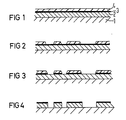
- a substrate 1 is used in each case, which can consist of a silicon dioxide layer which was formed on a semiconductor wafer (not shown) during manufacture. Usually contains one Semiconductor wafer at least one integrated circuit manufactured in a conventional manner including ohmic contacts (which are not shown).
- a metal oxide layer 3 is evaporated or sputtered over it.
- a layer 4 of a peelable mask material is applied over layer 3.
- This mask material is characterized as an organic, polymeric material, which can be, for example, a photoresist, an electron beam or X-ray sensitive lacquer, which is applied in the usual way, for example by spinning, as a coating (FIG. 1).
- the paint is structured in the usual way ( Figure 2).
- z. B. by reactive ion-beam etching the metal oxide 3 at the vacant locations structured without lacquer shrinkage ( Figure 3).
- the layer to be etched etched Figure 4).
Landscapes
- Physics & Mathematics (AREA)
- General Physics & Mathematics (AREA)
- Engineering & Computer Science (AREA)
- Architecture (AREA)
- Structural Engineering (AREA)
- Drying Of Semiconductors (AREA)
- ing And Chemical Polishing (AREA)
Claims (3)
Applications Claiming Priority (2)
| Application Number | Priority Date | Filing Date | Title |
|---|---|---|---|
| DE19813102647 DE3102647A1 (de) | 1981-01-27 | 1981-01-27 | Strukturierung von metalloxidmasken, insbesondere durch reaktives ionenstrahlaetzen |
| DE3102647 | 1981-01-27 |
Publications (3)
| Publication Number | Publication Date |
|---|---|
| EP0056845A2 EP0056845A2 (fr) | 1982-08-04 |
| EP0056845A3 EP0056845A3 (en) | 1982-09-01 |
| EP0056845B1 true EP0056845B1 (fr) | 1985-01-30 |
Family
ID=6123431
Family Applications (1)
| Application Number | Title | Priority Date | Filing Date |
|---|---|---|---|
| EP81108438A Expired EP0056845B1 (fr) | 1981-01-27 | 1981-10-16 | Réalisation d'un masque en oxyde métallique, en particulier par attaque ionique réactive |
Country Status (4)
| Country | Link |
|---|---|
| US (1) | US4390394A (fr) |
| EP (1) | EP0056845B1 (fr) |
| JP (1) | JPS57143830A (fr) |
| DE (1) | DE3102647A1 (fr) |
Families Citing this family (16)
| Publication number | Priority date | Publication date | Assignee | Title |
|---|---|---|---|---|
| JPS59202636A (ja) * | 1983-05-04 | 1984-11-16 | Hitachi Ltd | 微細パタ−ン形成方法 |
| JPH061769B2 (ja) * | 1983-08-10 | 1994-01-05 | 株式会社日立製作所 | アルミナ膜のパターニング方法 |
| JPS60133516A (ja) * | 1983-12-22 | 1985-07-16 | Hitachi Ltd | 薄膜磁気ヘツドの製造方法 |
| US4581099A (en) * | 1985-01-30 | 1986-04-08 | Canon Kabushiki Kaisha | Method for preparation of a photosensor |
| US4619894A (en) * | 1985-04-12 | 1986-10-28 | Massachusetts Institute Of Technology | Solid-transformation thermal resist |
| GB2189903A (en) * | 1986-04-01 | 1987-11-04 | Plessey Co Plc | An etch technique for metal mask definition |
| US5024724A (en) * | 1987-03-27 | 1991-06-18 | Sanyo Electric Co., Ltd. | Dry-etching method |
| FR2640809B1 (fr) * | 1988-12-19 | 1993-10-22 | Chouan Yannick | Procede de gravure d'une couche d'oxyde metallique et depot simultane d'un film de polymere, application de ce procede a la fabrication d'un transistor |
| TW451355B (en) * | 1996-09-10 | 2001-08-21 | United Microelectronics Corp | Method for increasing the etching selectivity |
| JPH1098100A (ja) * | 1996-09-20 | 1998-04-14 | Nec Corp | コンタクトホール/スルーホール形成方法 |
| US6287975B1 (en) * | 1998-01-20 | 2001-09-11 | Tegal Corporation | Method for using a hard mask for critical dimension growth containment |
| US6958295B1 (en) * | 1998-01-20 | 2005-10-25 | Tegal Corporation | Method for using a hard mask for critical dimension growth containment |
| JP3067737B2 (ja) * | 1998-05-18 | 2000-07-24 | 日本電気株式会社 | 酸化バナジウム膜のプラズマエッチング方法 |
| DE10234734A1 (de) * | 2002-07-30 | 2004-02-12 | Infineon Technologies Ag | Verwendung von Masken aus Metalloxiden zur Bearbeitung von Oberflächen bei der Herstellung von Mikrochips |
| CN112490131B (zh) * | 2020-11-27 | 2024-09-13 | 西安交通大学 | 一种基于刻蚀工艺的引线框架制备方法 |
| CN115148433A (zh) * | 2022-06-15 | 2022-10-04 | 无锡尚积半导体科技有限公司 | 一种提升f基氧化钒刻蚀形貌的方法 |
Family Cites Families (12)
| Publication number | Priority date | Publication date | Assignee | Title |
|---|---|---|---|---|
| JPS4840811B1 (fr) * | 1969-11-13 | 1973-12-03 | ||
| CA1009607A (en) * | 1972-11-29 | 1977-05-03 | Heinz Dimigen | Method of manufacturing etched structures in substrates by ion etching |
| US3925677A (en) * | 1974-04-15 | 1975-12-09 | Bell Telephone Labor Inc | Platinum oxide lithographic masks |
| US3975252A (en) * | 1975-03-14 | 1976-08-17 | Bell Telephone Laboratories, Incorporated | High-resolution sputter etching |
| JPS5851412B2 (ja) * | 1975-03-19 | 1983-11-16 | 株式会社日立製作所 | 半導体装置の微細加工方法 |
| FR2312114A1 (fr) * | 1975-05-22 | 1976-12-17 | Ibm | Attaque de materiaux par ions reactifs |
| JPS5812338B2 (ja) * | 1975-07-15 | 1983-03-08 | 凸版印刷株式会社 | ドライエツチングホウホウ |
| FR2399486A1 (fr) * | 1977-08-04 | 1979-03-02 | Comp Generale Electricite | Procede de gravure d'une couche metallique par attaque ionique |
| US4132586A (en) * | 1977-12-20 | 1979-01-02 | International Business Machines Corporation | Selective dry etching of substrates |
| JPS5593225A (en) * | 1979-01-10 | 1980-07-15 | Hitachi Ltd | Forming method of minute pattern |
| JPS5913592B2 (ja) * | 1979-06-22 | 1984-03-30 | 三菱電機株式会社 | エツチング方法 |
| US4211582A (en) * | 1979-06-28 | 1980-07-08 | International Business Machines Corporation | Process for making large area isolation trenches utilizing a two-step selective etching technique |
-
1981
- 1981-01-27 DE DE19813102647 patent/DE3102647A1/de not_active Withdrawn
- 1981-10-16 EP EP81108438A patent/EP0056845B1/fr not_active Expired
-
1982
- 1982-01-11 US US06/338,605 patent/US4390394A/en not_active Expired - Fee Related
- 1982-01-20 JP JP57007369A patent/JPS57143830A/ja active Pending
Non-Patent Citations (1)
| Title |
|---|
| IEEE Transactions on Electron Devices, Vol. ED-22, No. 7, Juli 1975, p. 483-486 * |
Also Published As
| Publication number | Publication date |
|---|---|
| EP0056845A3 (en) | 1982-09-01 |
| JPS57143830A (en) | 1982-09-06 |
| EP0056845A2 (fr) | 1982-08-04 |
| DE3102647A1 (de) | 1982-08-19 |
| US4390394A (en) | 1983-06-28 |
Similar Documents
| Publication | Publication Date | Title |
|---|---|---|
| EP0056845B1 (fr) | Réalisation d'un masque en oxyde métallique, en particulier par attaque ionique réactive | |
| DE2617914C2 (de) | Verfahren zum Herstellen von Mustern eines dünnen Films auf einem Substrat bei der Herstellung von integrierten Schaltungen | |
| DE2536718C3 (de) | Verfahren zur Herstellung geätzter Strukturen in Festkörperoberflächen durch Ionenätzung und Bestrahlungsmaske zur Verwendung in diesem Verfahren | |
| DE69308822T2 (de) | Verfahren zum Ätzen von Aluminium und dessen Legierungen unter Verwendung eines HC1, C1 und N2 enthaltenden Ätzmittels | |
| DE4107006C2 (fr) | ||
| DE2460988C2 (de) | Verfahren zum Niederschlagen eines Musters aus einem dünnen Film auf einem anorganischen Substrat | |
| DE2448535C2 (de) | Verfahren zum Niederschlagen dünner leitfähiger Filme auf einem anorganischen Substrat | |
| DE69023023T2 (de) | Röntgenstrahl-Maskenstruktur und Röntgenstrahl-Belichtungsverfahren. | |
| EP0002669B1 (fr) | Procédé pour enlever du matériau d'un substrat par gravure à sec sélective et emploi de ce procédé dans la production de patrons conducteurs | |
| DE3940087A1 (de) | Verfahren zur herstellung eines gemusterten gegenstands und danach hergestellter gegenstand | |
| DE2953117A1 (en) | Fabrication of integrated circuits utilizing thick high-resolution patterns | |
| DE2610014A1 (de) | Zerstaeubungsaetzen mit hoher aufloesung | |
| DE2754396A1 (de) | Verfahren zum herstellen von duennfilmmustern | |
| DE69837301T2 (de) | Methode, einen Platinfilm in einer Halbleiteranordnung zu ätzen | |
| DE4320033A1 (de) | Verfahren zur Bildung eines Metallmusters bei der Herstellung einer Halbleitereinrichtung | |
| DE4102422A1 (de) | Verfahren zur herstellung einer in mehreren ebenen angeordneten leiterstruktur einer halbleitervorrichtung | |
| DE2408235A1 (de) | Verfahren zur herstellung einer halbleiter-sonnenzelle | |
| DE2432719B2 (de) | Verfahren zum erzeugen von feinen strukturen aus aufdampfbaren materialien auf einer unterlage und anwendung des verfahrens | |
| DE19717363C2 (de) | Herstellverfahren für eine Platinmetall-Struktur mittels eines Lift-off-Prozesses und Verwendung des Herstellverfahrens | |
| EP0166893B1 (fr) | Procédé d'attaque chimique sèche | |
| DE2853295C2 (de) | Verfahren zum Herstellen einer Speicherplatte für ein Vidikon | |
| DE2504500A1 (de) | Verfahren zur herstellung eines musters aus einer oder mehreren schichten auf einer unterlage durch oertliche entfernung dieser schicht oder schichten durch sputteraetzen und gegenstaende, insbesondere halbleiteranordnungen, die unter verwendung dieses verfahrens hergestellt sind | |
| DE69201291T2 (de) | Musterbildungsverfahren. | |
| DE2703473C2 (fr) | ||
| EP0132823B1 (fr) | Procédé pour la fabrication de structures à dimensions stables à proportion d'aspect élévée, dans la région 1 millimicron et en dessous, pour la micro-éléctronique et emploi de ce procédé pour la fabrication de masques pour rayons-X |
Legal Events
| Date | Code | Title | Description |
|---|---|---|---|
| PUAI | Public reference made under article 153(3) epc to a published international application that has entered the european phase |
Free format text: ORIGINAL CODE: 0009012 |
|
| PUAL | Search report despatched |
Free format text: ORIGINAL CODE: 0009013 |
|
| 17P | Request for examination filed |
Effective date: 19811016 |
|
| AK | Designated contracting states |
Designated state(s): FR GB IT NL |
|
| AK | Designated contracting states |
Designated state(s): FR GB IT NL |
|
| ITF | It: translation for a ep patent filed | ||
| GRAA | (expected) grant |
Free format text: ORIGINAL CODE: 0009210 |
|
| AK | Designated contracting states |
Designated state(s): FR GB IT NL |
|
| ET | Fr: translation filed | ||
| PLBE | No opposition filed within time limit |
Free format text: ORIGINAL CODE: 0009261 |
|
| STAA | Information on the status of an ep patent application or granted ep patent |
Free format text: STATUS: NO OPPOSITION FILED WITHIN TIME LIMIT |
|
| 26N | No opposition filed | ||
| PGFP | Annual fee paid to national office [announced via postgrant information from national office to epo] |
Ref country code: NL Payment date: 19871031 Year of fee payment: 7 |
|
| PG25 | Lapsed in a contracting state [announced via postgrant information from national office to epo] |
Ref country code: NL Effective date: 19890501 |
|
| NLV4 | Nl: lapsed or anulled due to non-payment of the annual fee | ||
| PGFP | Annual fee paid to national office [announced via postgrant information from national office to epo] |
Ref country code: GB Payment date: 19910913 Year of fee payment: 11 |
|
| PGFP | Annual fee paid to national office [announced via postgrant information from national office to epo] |
Ref country code: FR Payment date: 19911022 Year of fee payment: 11 |
|
| ITTA | It: last paid annual fee | ||
| PG25 | Lapsed in a contracting state [announced via postgrant information from national office to epo] |
Ref country code: GB Effective date: 19921016 |
|
| GBPC | Gb: european patent ceased through non-payment of renewal fee |
Effective date: 19921016 |
|
| PG25 | Lapsed in a contracting state [announced via postgrant information from national office to epo] |
Ref country code: FR Effective date: 19930630 |
|
| REG | Reference to a national code |
Ref country code: FR Ref legal event code: ST |