EP0056856A1 - Verfahren zum Formen von PN-Übergangen, insbesondere in IGFET-Bauelementen, mit verbesserten Drain-Spannungs-Charakteristiken - Google Patents
Verfahren zum Formen von PN-Übergangen, insbesondere in IGFET-Bauelementen, mit verbesserten Drain-Spannungs-Charakteristiken Download PDFInfo
- Publication number
- EP0056856A1 EP0056856A1 EP81110106A EP81110106A EP0056856A1 EP 0056856 A1 EP0056856 A1 EP 0056856A1 EP 81110106 A EP81110106 A EP 81110106A EP 81110106 A EP81110106 A EP 81110106A EP 0056856 A1 EP0056856 A1 EP 0056856A1
- Authority
- EP
- European Patent Office
- Prior art keywords
- impurity
- concentration
- implanted
- substrate
- arsenic
- Prior art date
- Legal status (The legal status is an assumption and is not a legal conclusion. Google has not performed a legal analysis and makes no representation as to the accuracy of the status listed.)
- Granted
Links
Images

Classifications
-
- H—ELECTRICITY
- H10—SEMICONDUCTOR DEVICES; ELECTRIC SOLID-STATE DEVICES NOT OTHERWISE PROVIDED FOR
- H10P—GENERIC PROCESSES OR APPARATUS FOR THE MANUFACTURE OR TREATMENT OF DEVICES COVERED BY CLASS H10
- H10P30/00—Ion implantation into wafers, substrates or parts of devices
- H10P30/20—Ion implantation into wafers, substrates or parts of devices into semiconductor materials, e.g. for doping
- H10P30/202—Ion implantation into wafers, substrates or parts of devices into semiconductor materials, e.g. for doping characterised by the semiconductor materials
- H10P30/204—Ion implantation into wafers, substrates or parts of devices into semiconductor materials, e.g. for doping characterised by the semiconductor materials into Group IV semiconductors
-
- H—ELECTRICITY
- H10—SEMICONDUCTOR DEVICES; ELECTRIC SOLID-STATE DEVICES NOT OTHERWISE PROVIDED FOR
- H10D—INORGANIC ELECTRIC SEMICONDUCTOR DEVICES
- H10D30/00—Field-effect transistors [FET]
- H10D30/01—Manufacture or treatment
- H10D30/021—Manufacture or treatment of FETs having insulated gates [IGFET]
- H10D30/0223—Manufacture or treatment of FETs having insulated gates [IGFET] having source and drain regions or source and drain extensions self-aligned to sides of the gate
- H10D30/0227—Manufacture or treatment of FETs having insulated gates [IGFET] having source and drain regions or source and drain extensions self-aligned to sides of the gate having both lightly-doped source and drain extensions and source and drain regions self-aligned to the sides of the gate, e.g. lightly-doped drain [LDD] MOSFET or double-diffused drain [DDD] MOSFET
-
- H—ELECTRICITY
- H10—SEMICONDUCTOR DEVICES; ELECTRIC SOLID-STATE DEVICES NOT OTHERWISE PROVIDED FOR
- H10D—INORGANIC ELECTRIC SEMICONDUCTOR DEVICES
- H10D30/00—Field-effect transistors [FET]
- H10D30/60—Insulated-gate field-effect transistors [IGFET]
- H10D30/601—Insulated-gate field-effect transistors [IGFET] having lightly-doped drain or source extensions, e.g. LDD IGFETs or DDD IGFETs
- H10D30/605—Insulated-gate field-effect transistors [IGFET] having lightly-doped drain or source extensions, e.g. LDD IGFETs or DDD IGFETs having significant overlap between the lightly-doped extensions and the gate electrode
-
- H—ELECTRICITY
- H10—SEMICONDUCTOR DEVICES; ELECTRIC SOLID-STATE DEVICES NOT OTHERWISE PROVIDED FOR
- H10D—INORGANIC ELECTRIC SEMICONDUCTOR DEVICES
- H10D62/00—Semiconductor bodies, or regions thereof, of devices having potential barriers
- H10D62/10—Shapes, relative sizes or dispositions of the regions of the semiconductor bodies; Shapes of the semiconductor bodies
- H10D62/13—Semiconductor regions connected to electrodes carrying current to be rectified, amplified or switched, e.g. source or drain regions
- H10D62/149—Source or drain regions of field-effect devices
- H10D62/151—Source or drain regions of field-effect devices of IGFETs
-
- H—ELECTRICITY
- H10—SEMICONDUCTOR DEVICES; ELECTRIC SOLID-STATE DEVICES NOT OTHERWISE PROVIDED FOR
- H10P—GENERIC PROCESSES OR APPARATUS FOR THE MANUFACTURE OR TREATMENT OF DEVICES COVERED BY CLASS H10
- H10P30/00—Ion implantation into wafers, substrates or parts of devices
- H10P30/20—Ion implantation into wafers, substrates or parts of devices into semiconductor materials, e.g. for doping
- H10P30/21—Ion implantation into wafers, substrates or parts of devices into semiconductor materials, e.g. for doping of electrically active species
- H10P30/212—Through-implantation
Definitions
- This invention relates to methods of fabricating field- effect semiconductor devices and more particularly to a method of providing IGFET devices having junction depths of less than one pm which can sustain high voltages while possessing low sheet resistivity and low capacitance.
- IGFET source/drain junctions have been formed by thermal solid state diffusion techniques using various dopant sources. Recent trends to reduce the horizontal geometry of such devices have also required that vertical geometries also be reduced along with corresponding reductions in operating potentials and power. Very large scale integration techniques require IGFET junction depths on the order of 0.2 to 1.0 pm. Solid state diffusion techniques have proved to be unsuitable for the formation of such junctions because of a number of undesirable characteristics including the inability to provide adequately low sheet resistance with the required junction depths. In addition, impurity concentration profiles resulting from surface diffusion are often inadequately steep and result in increased junction capacitance as well as increased reverse bias leakage levels. Ion implantation is now preferred for providing source/drain regions in IGFETs as ion implantation enables better selection of impurity species, more accurate control of impurity concentration and profile and is particularly adapted to self-aligned processing techniques.
- ion implantation causes physical damage to the semiconductor crystal and thermal annealing of the implanted crystal becomes of prime importance in any ion implantation process. Remaining or residual damage, when made electrically active by precipitation effects can enhance reverse bias junction leakage if these defects lie near the p-n junction depletion region.
- a preferred technique therefore, has been to utilize ion implantation as a prediffusion source and to follow the ion implantation with a thermal diffusion/anneal process in order to enable the dopant species to diffuse beyond damaged crystal sites and become electrically active. Implant/diffusion processes are particularly important in those instances when a screen oxide is used to protect the silicon semiconductor surface from implant-introduced surface contamination, which provides an additional defect producing phenomenon caused by the presence of excess oxygen atoms in the crystal.
- arsenic has become the preferred n-type dopant species for making source/drain regions of n-channel polysilicon-gate IGFETs, primarily because of the ability to achieve relatively low resistivity shallow junction having low leakage characteristics in a simple implant/diffusion process.
- the reduction of device geometries also has some inherent limitations.
- the reduction in device size, particularly channel length causes a decrease in the drain voltage at which low-level avalanche, junction breakdown and/or punch-through occur, see for example the article "Drain Voltage Limitations of MOS Transistors" by I. M. Bateman et al in Solid-State Electronics, Vol. 17, pp. 539-550 (June 1974).
- Such drain voltage limitations impose restrictions on the design of IGFET devices with respect to one or more of: drain voltage supply, channel length, diffusion depth, diffusion concentration profile, substrate doping level, channel doping level, etc.
- the primary concern relating to source/drain region design is the ability to withstand various breakdown phenomena and to provide low leakage current.
- U.S. Patent 4 028 717 to Joy et al teaches a drain junction formed from concentric diffusions or ion implantation regions. A first low concentration region formed with a maximum concentration below the semiconductor surface effectively forms the drain electrode. A second high concentration region lies inside the first region and has a concentration peak near the semiconductor surface to provide a low resistivity contact to the first region. The two regions are defined separately and require separate mask and photoresist steps.
- U.S. Patent 4 070 687 to Ho teaches - a similar approach to the same problem but uses only one masking step. Here two dopants, arsenic and phosphorus are diffused or ion implanted to provide a high surface concentration and subsequently diffused to form an n+, p-, p junction due to the difference in diffusion rates.
- U.S. Patent 3 897 276 to Kondo may also be of interest as it teaches a double ion implantation method of forming a junction from as-implanted ions without subsequent diffusion in which a p+, p, n, n+ junction is formed in a semiconductor substrate.
- Ions of a relatively high atomic mass, indium are implanted at a low concentration relatively deep below the surface of a silicon substrate and at least one implant of a low mass ion, boron, of the same impurity type is implanted with a high concentration near the surface of the substrate to form an IMPATT diode.
- the p-n junction portion of the device is controlled by the smaller straggling range of the heavier ion in the substrate and thus provides a step-like concentration profile at the metallurgical junction.
- Yagi et al teaches the formation of the n+, n emitter region by the thermal diffusion of a high concentration of phosphorus into a 2 Qcm n-type epitaxial layer. Aggarwal suggests three alternative techniques for forming the emitter of Yagi et al.
- a first similar to Onodera above, uses sequential implantation and anneal steps of a shallow high concentration of arsenic followed by a deeper high concentration of phosphorus resulting in a composite n-type emitter at least several microns in depth.
- the second uses a single shallow implantation step of a high concentration of arsenic followed by thermal diffusion of a high concentration of phosphorus.
- the third uses a combination of the first but is annealed in a standard bipolar drive-in environment.
- U.S. Patent 3 812 519 to Nakamura et al is of interest as it relates to ion implantation techniques for forming high concentration bipolar emitter regions having reduced emitter dip effect by the surface diffusion of both arsenic and phosphorous having a concentration ratio, of arsenic to phosphorus atoms of from 4 to 40:100.
- the presence of the arsenic is intended to prevent lattice collapse, thus allowing a higher surface concentration to be achieved.
- Patent 4 111 719 to Mader et al teaches achieving a similar result in which a silicon substrate which has been ion implanted with arsenic at 80KeV with a dose of 2 x 10¹⁶ ions/cm 2 (hereafter such powers of 10 will be expressed as 2E16 ions/cm 2 ), resulting in a peak concentration of arsenic near the solid solubility of arsenic in silicon, is also implanted with germanium at a dose of 2 E15 ions/cm 2 at 75KeV and then annealed.
- junction formation techniques both to provide controlled dopant concentration profile for various types of devices and to provide improved junction quality by reduction of leakage causing defects of the crystalline structure in the vicinity of junctions
- the fabrication of shallow junctions of less than one micron depth with adequate low resistivity, high breakdown voltage, high sustaining voltage, low capacitance and low reverse bias leakage suitable for use in forming junctions in very large scale integrated circuit IGFET devices has not been provided.
- this invention intends to provide junction regions with a junction depth of less than one pm having all of the desired properties for use in very large scale integrated circuits which are capable of operating reliably under higher voltages.
- This invention also intends to improve IGFET devices for operation at higher supply potentials.
- a first conductivity determining impurity ion of a first type is implanted into a substrate of a second type through a screen oxide. This provides a maximum impurity concentration at the oxide/substrate interface of a magnitude in excess of that required to achieve maximum electrical solubility of the impurity in the substrate.
- a second conductivity determining impurity ion of the first type is also implanted through the screen oxide to provide a maximum concentration at a depth below that of the first impurity and having a maximum concentration at least one order of magnitude less than that of the first impurity.
- An oxidizing drive-in annealing process causes thermal diffusion of both of the implanted impurities to provide a junction having a first portion of its electrically active concentration profile equal to that of the maximum electrical solubility of the first impurity in the substrate which extends to a depth greater than that of the maximum concentration of the second impurity as-implanted, a second portion of lower concentration determined by the first and second impurities which substantially determines the electrical breakdown characteristics of the junction, and a third portion determined by the second impurity.
- Arsenic and phosphorus are preferred as the first and second impurities, respectively.
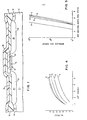
- FIG. 1 illustrates a typical IGFET device fabricated by the process, although any similar process having more or less features may also be used to practice the invention.
- the preferred process may be implemented as follows. Starting with a boron doped silicon semiconductor wafer 10, of about 12 Q cm resistivity and having its major surface parallel to the 100 crystalline plane, a thin thermal silicon dioxide layer is grown followed by the chemical vapor deposition of a silicon nitride layer. This composite layer is patterned by known photolithographic masking and etching techniques to remove the silicon nitride in areas where devices are to be formed.
- a field threshold voltage tailoring step is performed by ion implanting boron ions at an energy of about 80 to 150 KeV and a dosage of about 1 to 5E13 ions/cm 2 . This is followed by the thermal oxidation of the wafer in a dry-wet-dry oxidation atmosphere to provide about 5000 to 10,000 R of semi-recessed dielectric oxide 12, generally referred to as ROX, in all areas of the wafer not protected by the previously defined silicon nitride layer.
- the ion implanted boron diffuses faster than the surface of the wafer is oxidized to provide p+ type semiconductor regions 14 under ROX regions 12 which act as channel stoppers between active device areas by raising the inversion threshold voltage under the ROX areas.
- oxide/ nitride masking layer is then removed by etching followed by the thermal growth of 150 to 800 R of silicon dioxide which will act as the gate insulator layer 16.
- boron is next ion implanted at an energy of about 30 to 100 KeV and a dose of about lEll to 2E12 ions/cm 2 , as represented by the small x's 18 in the channel region.
- phosphorus doped polysilicon is deposited by chemical vapor deposition to a thickness of about 1000 to 5000 R.
- a layer of pyrolytic silicon dioxide may be deposited at this point followed by patterned etching of the oxide covered polysilicon, removal of thin thermal oxide not protected by oxidized polysilicon, subsequent thermal oxidation of the substrate surface and exposed polysilicon edges and deposition of a second doped polysilicon layer.
- the last deposited layer of polysilicon is etched to form IGEET gate electrodes 20 retaining or removing and regrowing the gate dielectric over remaining portions of the substrate to act as an ion implantation screen in the next step.
- Source and drain regions are next formed by the two-step ion implantation/drive-in process using both the polysilicon and ROX areas as a mask.
- arsenic ions implanted at an energy of about 20 to 120 KeV, depending upon the gate insulator/screen oxide thickness, with a dose of 3E15 to 1.2E16 ions/cm 2 followed by an oxidizing drive-in process will provide satisfactory source/drain regions having a junction depth of less than 1.0 ⁇ m.
- the oxidation process provides an oxide layer 24 over polysilicon gate electrode 20 and implanted source/drain regions.
- the drive-in process is followed by deposition of passivating phosphorus doped glass layer 26 followed by an anneal step in nitrogen.
- the resulting junctions 22 provide adequate electrical breakdown and leakage characteristics for use in integrated circuits powered by drain supply voltage on the order of about 5.0 V.
- control or standard arsenic process steps related specifically to the source drain junction formation consisted of the following steps.
- step 2 The other experiment wafers were made by modifying step 2 as follows:
- the arsenic energy is intended to provide a peak concentration at the screen oxide-silicon interface so that subsequent thermal diffusion would determine the final concentration profile at a depth below that in which substantial crystal damage occurs by the arsenic implant process.
- the phosphorus energy was selected to give a projected range of 1757 R with a sigma of 595 ⁇ . Reasons for selecting this energy were twofold. First, the range must be limited such that the phosphorus does not penetrate the polysilicon gate and the gate oxide which would alter the IGFET threshold voltage. Second, it was desired to implant the phosphorus significantly below the arsenic implant in order to aid in its diffusion beyond the expected arsenic metallurgical junction.
- FIG. 2 Ions which are theoretically predicted to lie outside the target surface, as shown by dashed lines, are assumed to accumulate at the surface, increasing the ion density there above the Gaussian prediction.
- the peak arsenic concentration for arsenic lies at the interface between the screen oxide and the silicon surface and is substantially at or above the maximum solid solubility of arsenic in silicon.
- the peak phosphorus concentration lies considerably deeper in the silicon and is about three orders of magnitude less than that of the arsenic and about two orders of magnitude greater than the background concentration of acceptors in the bulk portion of the wafer.
- junction dopant concentration profiles taken by the spreading resistance technique for arsenic alone and the two low dose arsenic plus phosphorus, Groups B and C are shown in FIG. 3.
- the metallurgical junction depths were measured at 0.46, 0.65 and 0.73 ⁇ m, respectively for each group. Electrically the junction depths may appear shallower than the metallurgical junction due to the depletion of carriers during normal reverse biased operation of devices.
- the depth at which the donor level drops below that of the acceptors in the implanted channel region is about 0.46, 0.58, and 0.67 pm respectively.
- the arsenic plus phosphorus diffusion profiles also show compensation of the background boron concentration near the junction which does not appear on the arsenic profile.
- FIG. 4 shows the effect on minimum sustaining voltage, Vss, versus effective channel length, Leff, for all groups except that for the double arsenic implant.
- Vss minimum sustaining voltage
- Leff effective channel length
- Table I exhibits some additional electrical characteristics determined from test data and shows no substantial difference in channel shortening L as indicated in the second column, a decrease in sheet resistivity with increasing phosphorus dose and an increase in junction breakdown voltage to ROX, VBPN.
- gated breakdown voltage at the channel side of the drain diffusion also shows an improvement similar to that of VBPN. There was no significant difference in threshold voltage lowering for short channel devices despite the increase in junction depths :.n the arsenic plus phosphorus wafers.
- junction area capacitance measurements showed a 0 to 5 percent decrease for the two lower dose phosphorus groups over that of the standard arsenic wafers. Junction to adjacent ROX capacitance was found to increase 5-10 percent for the two low dose phosphorus wafers. This is most likely due to the deeper junctions causing an increase in the sidewall area between the diffusions and the p+ regions under the ROX, therefore increasing total capacitance which is not compensated by the reduction in capacitance per unit of sidewall area caused by the more graded junction doping profile.
- Fig. 5 The effect of the arsenic plus phosphorus on channel hot electron sensitivity is shown in Fig. 5 where normalized gate current is plotted versus gate and drain to substrate bias voltage. All of the arsenic plus phosphorus groups B-E show an increase in about 1 V gate/drain bias for a fixed gate current over that of arsenic alone. Thus, IGFET device threshold shifts due to hot electron effects will be reduced significantly.
Landscapes
- Insulated Gate Type Field-Effect Transistor (AREA)
Applications Claiming Priority (2)
| Application Number | Priority Date | Filing Date | Title |
|---|---|---|---|
| US06/227,567 US4369072A (en) | 1981-01-22 | 1981-01-22 | Method for forming IGFET devices having improved drain voltage characteristics |
| US227567 | 1981-01-22 |
Publications (2)
| Publication Number | Publication Date |
|---|---|
| EP0056856A1 true EP0056856A1 (de) | 1982-08-04 |
| EP0056856B1 EP0056856B1 (de) | 1986-03-05 |
Family
ID=22853600
Family Applications (1)
| Application Number | Title | Priority Date | Filing Date |
|---|---|---|---|
| EP81110106A Expired EP0056856B1 (de) | 1981-01-22 | 1981-12-03 | Verfahren zum Formen von PN-Übergangen, insbesondere in IGFET-Bauelementen, mit verbesserten Drain-Spannungs-Charakteristiken |
Country Status (4)
| Country | Link |
|---|---|
| US (1) | US4369072A (de) |
| EP (1) | EP0056856B1 (de) |
| JP (1) | JPS57134974A (de) |
| DE (1) | DE3174014D1 (de) |
Cited By (2)
| Publication number | Priority date | Publication date | Assignee | Title |
|---|---|---|---|---|
| DE3342773A1 (de) * | 1983-11-25 | 1985-06-05 | Siemens AG, 1000 Berlin und 8000 München | Verfahren zum herstellen von spannungsfesten mos-feldeffekttransistoren mit weichen konzentrationsprofilen am drain-uebergang |
| WO1990010309A3 (en) * | 1989-03-02 | 1991-01-24 | Thunderbird Tech Inc | Fermi threshold field effect transistor |
Families Citing this family (29)
| Publication number | Priority date | Publication date | Assignee | Title |
|---|---|---|---|---|
| DE3133841A1 (de) * | 1981-08-27 | 1983-03-17 | Siemens AG, 1000 Berlin und 8000 München | Verfahren zum herstellen von hochintegrierten komplementaeren mos-feldeffekttransistorschaltungen |
| US5389809A (en) * | 1982-02-01 | 1995-02-14 | Texas Instruments Incorporated | Silicided MOS transistor |
| US4566175A (en) * | 1982-08-30 | 1986-01-28 | Texas Instruments Incorporated | Method of making insulated gate field effect transistor with a lightly doped drain using oxide sidewall spacer and double implantations |
| US4519127A (en) * | 1983-02-28 | 1985-05-28 | Tokyo Shibaura Denki Kabushiki Kaisha | Method of manufacturing a MESFET by controlling implanted peak surface dopants |
| US4710477A (en) * | 1983-09-12 | 1987-12-01 | Hughes Aircraft Company | Method for forming latch-up immune, multiple retrograde well high density CMOS FET |
| US4621411A (en) * | 1984-09-28 | 1986-11-11 | Texas Instruments Incorporated | Laser-enhanced drive in of source and drain diffusions |
| KR940006668B1 (ko) * | 1984-11-22 | 1994-07-25 | 가부시끼가이샤 히다찌세이사꾸쇼 | 반도체 집적회로 장치의 제조방법 |
| US4590665A (en) * | 1984-12-10 | 1986-05-27 | Solid State Scientific, Inc. | Method for double doping sources and drains in an EPROM |
| US4851360A (en) * | 1986-09-29 | 1989-07-25 | Texas Instruments Incorporated | NMOS source/drain doping with both P and As |
| US5021851A (en) * | 1988-05-03 | 1991-06-04 | Texas Instruments Incorporated | NMOS source/drain doping with both P and As |
| US5047357A (en) * | 1989-02-03 | 1991-09-10 | Texas Instruments Incorporated | Method for forming emitters in a BiCMOS process |
| JPH0362568A (ja) * | 1989-07-31 | 1991-03-18 | Hitachi Ltd | 半導体装置の製造方法 |
| US5330922A (en) * | 1989-09-25 | 1994-07-19 | Texas Instruments Incorporated | Semiconductor process for manufacturing semiconductor devices with increased operating voltages |
| JPH03105295U (de) * | 1989-12-20 | 1991-10-31 | ||
| JP2626289B2 (ja) * | 1990-03-27 | 1997-07-02 | 松下電器産業株式会社 | 半導体装置の製造方法 |
| US5244823A (en) * | 1991-05-21 | 1993-09-14 | Sharp Kabushiki Kaisha | Process for fabricating a semiconductor device |
| US5885877A (en) * | 1997-04-21 | 1999-03-23 | Advanced Micro Devices, Inc. | Composite gate electrode incorporating dopant diffusion-retarding barrier layer adjacent to underlying gate dielectric |
| US6080629A (en) * | 1997-04-21 | 2000-06-27 | Advanced Micro Devices, Inc. | Ion implantation into a gate electrode layer using an implant profile displacement layer |
| US6380055B2 (en) | 1998-10-22 | 2002-04-30 | Advanced Micro Devices, Inc. | Dopant diffusion-retarding barrier region formed within polysilicon gate layer |
| US6329704B1 (en) * | 1999-12-09 | 2001-12-11 | International Business Machines Corporation | Ultra-shallow junction dopant layer having a peak concentration within a dielectric layer |
| US7332750B1 (en) | 2000-09-01 | 2008-02-19 | Fairchild Semiconductor Corporation | Power semiconductor device with improved unclamped inductive switching capability and process for forming same |
| US20040121524A1 (en) * | 2002-12-20 | 2004-06-24 | Micron Technology, Inc. | Apparatus and method for controlling diffusion |
| US7297617B2 (en) * | 2003-04-22 | 2007-11-20 | Micron Technology, Inc. | Method for controlling diffusion in semiconductor regions |
| US7419892B2 (en) * | 2005-12-13 | 2008-09-02 | Cree, Inc. | Semiconductor devices including implanted regions and protective layers and methods of forming the same |
| US7995384B2 (en) | 2008-08-15 | 2011-08-09 | Macronix International Co., Ltd. | Electrically isolated gated diode nonvolatile memory |
| US9685335B2 (en) | 2012-04-24 | 2017-06-20 | Fairchild Korea Semiconductor Ltd. | Power device including a field stop layer |
| US20130277793A1 (en) | 2012-04-24 | 2013-10-24 | Fairchild Korea Semiconductor, Ltd. | Power device and fabricating method thereof |
| US10181513B2 (en) | 2012-04-24 | 2019-01-15 | Semiconductor Components Industries, Llc | Power device configured to reduce electromagnetic interference (EMI) noise |
| US11869956B2 (en) * | 2021-09-30 | 2024-01-09 | Texas Instruments Incorporated | Channel stop and well dopant migration control implant for reduced MOS threshold voltage mismatch |
Citations (3)
| Publication number | Priority date | Publication date | Assignee | Title |
|---|---|---|---|---|
| US4028717A (en) * | 1975-09-22 | 1977-06-07 | Ibm Corporation | Field effect transistor having improved threshold stability |
| EP0013340A1 (de) * | 1978-12-28 | 1980-07-23 | International Business Machines Corporation | Widerstand mit verbesserter Durchbruchspannung, hergestellt durch eine doppelte Ionenimplantation in einem Halbleitersubstrat, und dessen Herstellungsverfahren |
| GB2046993A (en) * | 1979-03-29 | 1980-11-19 | Siemens Ag | Process for producing an mis-field effect transistor |
Family Cites Families (18)
| Publication number | Priority date | Publication date | Assignee | Title |
|---|---|---|---|---|
| US3879230A (en) * | 1970-02-07 | 1975-04-22 | Tokyo Shibaura Electric Co | Semiconductor device diffusion source containing as impurities AS and P or B |
| US3812519A (en) * | 1970-02-07 | 1974-05-21 | Tokyo Shibaura Electric Co | Silicon double doped with p and as or b and as |
| DE2104752B2 (de) * | 1971-02-02 | 1975-02-20 | Philips Patentverwaltung Gmbh, 2000 Hamburg | Verfahren zum Herstellen einer Halbleiter-Kapazitätsdiode |
| US3798079A (en) * | 1972-06-05 | 1974-03-19 | Westinghouse Electric Corp | Triple diffused high voltage transistor |
| JPS4924361A (de) * | 1972-06-27 | 1974-03-04 | ||
| US4079402A (en) * | 1973-07-09 | 1978-03-14 | National Semiconductor Corporation | Zener diode incorporating an ion implanted layer establishing the breakdown point below the surface |
| US4099998A (en) * | 1975-11-03 | 1978-07-11 | General Electric Company | Method of making zener diodes with selectively variable breakdown voltages |
| GB1569897A (en) * | 1975-12-31 | 1980-06-25 | Ibm | Field effect transistor |
| US4111719A (en) * | 1976-12-06 | 1978-09-05 | International Business Machines Corporation | Minimization of misfit dislocations in silicon by double implantation of arsenic and germanium |
| US4106953A (en) * | 1976-12-28 | 1978-08-15 | Motorola, Inc. | Method of producing an ion implanted tuning diode |
| US4133704A (en) * | 1977-01-17 | 1979-01-09 | General Motors Corporation | Method of forming diodes by amorphous implantations and concurrent annealing, monocrystalline reconversion and oxide passivation in <100> N-type silicon |
| US4111720A (en) * | 1977-03-31 | 1978-09-05 | International Business Machines Corporation | Method for forming a non-epitaxial bipolar integrated circuit |
| US4133701A (en) * | 1977-06-29 | 1979-01-09 | General Motors Corporation | Selective enhancement of phosphorus diffusion by implanting halogen ions |
| US4144100A (en) * | 1977-12-02 | 1979-03-13 | General Motors Corporation | Method of low dose phoshorus implantation for oxide passivated diodes in <10> P-type silicon |
| DE2802838A1 (de) * | 1978-01-23 | 1979-08-16 | Siemens Ag | Mis-feldeffekttransistor mit kurzer kanallaenge |
| DE2917455A1 (de) * | 1979-04-30 | 1980-11-13 | Ibm Deutschland | Verfahren zur vollstaendigen ausheilung von gitterdefekten in durch ionenimplantation von phosphor erzeugten n-leitenden zonen einer siliciumhalbleitervorrichtung und zugehoerige siliciumhalbleitervorrichtung |
| GB2056168A (en) * | 1979-08-01 | 1981-03-11 | Gen Instrument Corp | Method of fabricating P-N junction with high breakdown voltage |
| US4306916A (en) * | 1979-09-20 | 1981-12-22 | American Microsystems, Inc. | CMOS P-Well selective implant method |
-
1981
- 1981-01-22 US US06/227,567 patent/US4369072A/en not_active Expired - Lifetime
- 1981-12-03 DE DE8181110106T patent/DE3174014D1/de not_active Expired
- 1981-12-03 EP EP81110106A patent/EP0056856B1/de not_active Expired
- 1981-12-08 JP JP56196392A patent/JPS57134974A/ja active Granted
Patent Citations (3)
| Publication number | Priority date | Publication date | Assignee | Title |
|---|---|---|---|---|
| US4028717A (en) * | 1975-09-22 | 1977-06-07 | Ibm Corporation | Field effect transistor having improved threshold stability |
| EP0013340A1 (de) * | 1978-12-28 | 1980-07-23 | International Business Machines Corporation | Widerstand mit verbesserter Durchbruchspannung, hergestellt durch eine doppelte Ionenimplantation in einem Halbleitersubstrat, und dessen Herstellungsverfahren |
| GB2046993A (en) * | 1979-03-29 | 1980-11-19 | Siemens Ag | Process for producing an mis-field effect transistor |
Non-Patent Citations (1)
| Title |
|---|
| IBM Journal of Research and Development, Vol. 24, No. 3, May 1980 New York GEIPEL et al. "Implanted Source/Drain Junctions for Polysilicon Gate Technologies" pages 362 to 369 * |
Cited By (2)
| Publication number | Priority date | Publication date | Assignee | Title |
|---|---|---|---|---|
| DE3342773A1 (de) * | 1983-11-25 | 1985-06-05 | Siemens AG, 1000 Berlin und 8000 München | Verfahren zum herstellen von spannungsfesten mos-feldeffekttransistoren mit weichen konzentrationsprofilen am drain-uebergang |
| WO1990010309A3 (en) * | 1989-03-02 | 1991-01-24 | Thunderbird Tech Inc | Fermi threshold field effect transistor |
Also Published As
| Publication number | Publication date |
|---|---|
| JPS57134974A (en) | 1982-08-20 |
| EP0056856B1 (de) | 1986-03-05 |
| DE3174014D1 (en) | 1986-04-10 |
| JPH0231497B2 (de) | 1990-07-13 |
| US4369072A (en) | 1983-01-18 |
Similar Documents
| Publication | Publication Date | Title |
|---|---|---|
| EP0056856B1 (de) | Verfahren zum Formen von PN-Übergangen, insbesondere in IGFET-Bauelementen, mit verbesserten Drain-Spannungs-Charakteristiken | |
| US4717683A (en) | CMOS process | |
| EP0090940B1 (de) | Verfahren zum Herstellen von Emitter- und intrinsic-Basisgebieten eines bipolaren Transistors | |
| US8067805B2 (en) | Ultra shallow junction formation by epitaxial interface limited diffusion | |
| US5041885A (en) | Surface field effect transistor with depressed source and/or drain areas for ULSI integrated devices | |
| KR100822228B1 (ko) | 반도체 장치 및 그 제조 방법 | |
| US5268317A (en) | Method of forming shallow junctions in field effect transistors | |
| US5571744A (en) | Defect free CMOS process | |
| US4373252A (en) | Method for manufacturing a semiconductor structure having reduced lateral spacing between buried regions | |
| EP0852394B1 (de) | Verfahren zum Herstellen von flachen Übergängen in Siliziumbauelementen | |
| US4329773A (en) | Method of making low leakage shallow junction IGFET devices | |
| EP0258148A2 (de) | Veränderung der Eigenschaften eines P-Typ-Dotierungsstoffes mittels eines anderen P-Typ-Dotierungsstoffes | |
| Michel et al. | Annealing properties of ion‐implanted p‐n junctions in silicon | |
| US5453389A (en) | Defect-free bipolar process | |
| US7105413B2 (en) | Methods for forming super-steep diffusion region profiles in MOS devices and resulting semiconductor topographies | |
| US4472212A (en) | Method for fabricating a semiconductor device | |
| US4362574A (en) | Integrated circuit and manufacturing method | |
| US6855618B2 (en) | Radiation hardened semiconductor device | |
| US5420051A (en) | Pre-poly emitter implant | |
| US6054374A (en) | Method of scaling dielectric thickness in a semiconductor process with ion implantation | |
| US5208168A (en) | Semiconductor device having punch-through protected buried contacts and method for making the same | |
| EP0182876B1 (de) | Drei-wannen cmos-technologie | |
| KR100212010B1 (ko) | 반도체 소자의 트랜지스터 제조방법 | |
| US4814290A (en) | Method for providing increased dopant concentration in selected regions of semiconductor devices | |
| USRE35827E (en) | Surface field effect transistor with depressed source and/or drain areas for ULSI integrated devices |
Legal Events
| Date | Code | Title | Description |
|---|---|---|---|
| PUAI | Public reference made under article 153(3) epc to a published international application that has entered the european phase |
Free format text: ORIGINAL CODE: 0009012 |
|
| AK | Designated contracting states |
Designated state(s): DE FR GB IT |
|
| 17P | Request for examination filed |
Effective date: 19821116 |
|
| GRAA | (expected) grant |
Free format text: ORIGINAL CODE: 0009210 |
|
| AK | Designated contracting states |
Kind code of ref document: B1 Designated state(s): DE FR GB IT |
|
| PG25 | Lapsed in a contracting state [announced via postgrant information from national office to epo] |
Ref country code: IT Free format text: LAPSE BECAUSE OF FAILURE TO SUBMIT A TRANSLATION OF THE DESCRIPTION OR TO PAY THE FEE WITHIN THE PRESCRIBED TIME-LIMIT;WARNING: LAPSES OF ITALIAN PATENTS WITH EFFECTIVE DATE BEFORE 2007 MAY HAVE OCCURRED AT ANY TIME BEFORE 2007. THE CORRECT EFFECTIVE DATE MAY BE DIFFERENT FROM THE ONE RECORDED. Effective date: 19860305 |
|
| ET | Fr: translation filed | ||
| REF | Corresponds to: |
Ref document number: 3174014 Country of ref document: DE Date of ref document: 19860410 |
|
| PLBE | No opposition filed within time limit |
Free format text: ORIGINAL CODE: 0009261 |
|
| STAA | Information on the status of an ep patent application or granted ep patent |
Free format text: STATUS: NO OPPOSITION FILED WITHIN TIME LIMIT |
|
| 26N | No opposition filed | ||
| PGFP | Annual fee paid to national office [announced via postgrant information from national office to epo] |
Ref country code: DE Payment date: 20001201 Year of fee payment: 20 |
|
| PGFP | Annual fee paid to national office [announced via postgrant information from national office to epo] |
Ref country code: GB Payment date: 20001204 Year of fee payment: 20 |
|
| PGFP | Annual fee paid to national office [announced via postgrant information from national office to epo] |
Ref country code: FR Payment date: 20001220 Year of fee payment: 20 |
|
| PG25 | Lapsed in a contracting state [announced via postgrant information from national office to epo] |
Ref country code: GB Free format text: LAPSE BECAUSE OF EXPIRATION OF PROTECTION Effective date: 20011202 |
|
| REG | Reference to a national code |
Ref country code: GB Ref legal event code: PE20 Effective date: 20011202 |