EP0057557B1 - Schreibverfahren in einem statischen Halbleiterspeicher - Google Patents
Schreibverfahren in einem statischen Halbleiterspeicher Download PDFInfo
- Publication number
- EP0057557B1 EP0057557B1 EP82300382A EP82300382A EP0057557B1 EP 0057557 B1 EP0057557 B1 EP 0057557B1 EP 82300382 A EP82300382 A EP 82300382A EP 82300382 A EP82300382 A EP 82300382A EP 0057557 B1 EP0057557 B1 EP 0057557B1
- Authority
- EP
- European Patent Office
- Prior art keywords
- transistor
- writing
- transistors
- level
- signal
- Prior art date
- Legal status (The legal status is an assumption and is not a legal conclusion. Google has not performed a legal analysis and makes no representation as to the accuracy of the status listed.)
- Expired
Links
Images


Classifications
-
- G—PHYSICS
- G11—INFORMATION STORAGE
- G11C—STATIC STORES
- G11C11/00—Digital stores characterised by the use of particular electric or magnetic storage elements; Storage elements therefor
- G11C11/21—Digital stores characterised by the use of particular electric or magnetic storage elements; Storage elements therefor using electric elements
- G11C11/34—Digital stores characterised by the use of particular electric or magnetic storage elements; Storage elements therefor using electric elements using semiconductor devices
- G11C11/40—Digital stores characterised by the use of particular electric or magnetic storage elements; Storage elements therefor using electric elements using semiconductor devices using transistors
- G11C11/41—Digital stores characterised by the use of particular electric or magnetic storage elements; Storage elements therefor using electric elements using semiconductor devices using transistors forming static cells with positive feedback, i.e. cells not needing refreshing or charge regeneration, e.g. bistable multivibrator or Schmitt trigger
- G11C11/413—Auxiliary circuits, e.g. for addressing, decoding, driving, writing, sensing, timing or power reduction
- G11C11/414—Auxiliary circuits, e.g. for addressing, decoding, driving, writing, sensing, timing or power reduction for memory cells of the bipolar type
- G11C11/416—Read-write [R-W] circuits
Definitions
- the present invention relates to a method and a circuit for writing data in a static semiconductor memory device.
- DE-A-2947764 discloses a bipolar type static RAM (random access memory), comprising static memory cells connected at intersections of a plurality of word lines and pairs of bit lines, in which writing is effected by changing potentials of paired bit lines according to writing data of binary digits "1" and "0" and turning on one transistor of a memory cell while turning off the other transistor of the memory cell, emitters of the transistors of the memory cell connected to the bit lines respectively.
- Each memory cell is formed by a flip-flop circuit including two transistors, wherein if one transistor is in the ON state, the other is in the off state.
- the bit lines are connected to readout transistors, the emitters of which are commonly connected to a constant current source, the bases of which are respectively connected to the bit lines, and the ON and OFF state of the readout transistors is sensed by a sense amplifier.
- Writing is carried out by turning ON the transistor of the memory cell which is in the OFF state and by further turning OFF the transistor of the memory cell which is in ON state.
- a writing circuit comprising a pair of write-in transistors having emitters connected to the bit lines respectively, and a write amplifier whose outputs are connected to the bases of the write-in transistors; and according to the said writing data, one of the outputs is maintained at a low level while the other output is simultaneously maintained at a high level.
- one bit line is placed at a low potential level and the other bit line is placed at a high potential level.
- the waveforms of potentials in various parts of the memory cell are accompanied by vibration.
- potentials applied to the write bit line amplifier are returned to the readout level after completion of writing, they do not immediately change to the readout level, but first undergo damping vibrations for a while and then settle down.
- the readout mode is produced in the memory on completion of writing and as any such vibrations will create a whisker-like peak in the output of the sense amplifier, there is a risk of error by such a peak when reading is effected just after writing.
- Such a whisker-like peak is caused by vibrations generated when one potential at a bit line falls and the other potential at another bit line rises. Especially large vibrations are generated when the potential falls.
- An object of the present invention is to provide a method for writing in a semiconductor memory device in which the time required for writing can be shortened and adverse characteristics such as the generation of such a whisker-like peak are not caused after writing.
- the period of maintenance of the high level is shorter than the period of maintenance of the low level.
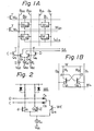
- a bipolar type static RAM comprises memory cells M oo , M oi , ... arranged in the form of a matrix, each memory cell consisting of a flip-flop, said memory cells being connected to word lines W o , W,, ... and bit lines B o , B,, ....
- W o h and W,h represent negative side word lines or hold lines
- B oo , B 01 and other similar symbols attached to the word lines "0" means a left bit line and "1" means a right bit line in the bit lines used in a pair.
- Fig. 1B is a view showing an example of the memory cells M oo , M o , ..., and the example shown comprises load resistors R, and R 2 and multiemitter transistors Q, and Q 2 .
- the memory cell is a flip-flop, if one transistor is turned on, the other transistor is turned off. Supposing that the transistor Q, is in the on state and the transistor Q 2 is in the off state, the potential at the point A is maintained at a low (L) level and the potential at the point B is maintained at a high (H) level.
- the selected word line is maintained at a high level, for example, V cc , which changes potential level at the point B to substantially V cc and the potential at the point A to V cc less the voltage drop of the load resistor.
- the transistor Q since the transistor Q, is turned on and the potential at the point B is at a high level, the bit line B o is maintained at a high level and the bit line B 1 is maintained at a low level.
- the transistors Q 3 and Q 4 of which emitters are commonly connected to a constant current source 1 0 , form a current switch type differential amplifier, wherein when the transistor Q 3 is turned on, the transistor Q 4 is turned off. Such an on-off state is detected by a sense amplifier SA to produce an output for reading out data stored in the cell.
- FIG 2 which illustrates a conventional write amplifier
- Q 11 through Q 13 represent transistors
- I 4 reprsents a constant current source
- D 1 and D 2 represent diodes
- d and d represent signals which are turned to high and low levels according to writing data "1" and "0". Supposing that the signals d and d are turned to high and low levels, in the case of data "1", respectively, the levels of the signals d and d are reversed in case of data "0".
- the write enable signal WE is maintained at a high level, and, therefore, the transistor Q, 3 is turned on and both the outputs C and D are maintained at the same level (the readout level RL).
- Writing is accomplished by turning on the transistor of the memory cell which is in the off state or further turning off the transistor of the memory cell which is in the on state.
- the transistor Q 2 is turned on, with the result that the transistor Q 1 is turned off to effect inversion of the state, that is, writing.
- the signal WE is maintained at a low level and the transistor Q 13 is turned off.
- one of the transistors Q " and Q 12 is turned on while the other transistor is turned off, with the result that one of the outputs C and D is maintained at a high level and the other output is maintained at a low level.
- 1/2 of the current of the constant current source 1 4 flows through the load resistor, diodes D, and D 2 , and transistors Q 11 and Q, 2 to cause reduction of the voltage in the load resistor.
- all of said current flows in the load resistor or said current does not flow in the load resistor at all (change of the current). Accordingly, the readout level RL and the high and low levels H and L at the time of writing are as shown in Fig. 3A.
- potential waveforms of the high and low levels H and L are accompanied by vibrations. That is, as shown in the right portion of Fig. 3A, when potentials C and D are returned to the readout level RL on completion of writing, they are not immediately changed to the level RL, but first undergo damping vibrations for a while and then settle down. As the readout mode is produced in the memory on completion of writing and as any such vibrations will create a whisker-like peak P as shown in Fig. 3B in the output of the sense amplifier, there is a risk of error by such a peak when reading is effected just after writing. Such a whisker-like peak is caused by vibrations generated when the potential C falls and the potential D rises. Especially large vibrations are generated when the potential falls.
- Writing can also the performed by turning one potential D, that is, the potential of the bit line B, to the low level as shown in Fig. 3C.
- D that is, the potential of the bit line B
- Fig. 3C the generation of vibration is relatively controlled, but this method is defective in that the time required for writing is long compared with the method shown in Fig. 3B. That is, reduction of the potential of one bit line and simultaneously elevation of the potential of the other bit line as shown in Fig. 3A, increases the writing speed and enables a smaller writing pulse width PW than in the method shown in Fig. 3C when only the potential of one bit line is reduced.
- one of the paired bit lines is maintained at a low level (L) while the other bit line is maintained at a high level (H).
- This high level is maintained only in the initial stage and is returned to the readout level RL while the low level of the other bit line is still maintained.
- Adoption of this arrangement allows the vibrations caused by falling to be completed during the writing operation, whereas such vibrations do not affect the bit line level just after completion of the writing operation.
- a certain high level period is ensured, turning-off of the transistor which has been in the on state can be performed positively, and, hence, the time required for writing can be shortened. It is sufficient if the period of the high level is several nsec.
- the period of the low level that is, the writing time
- the writing time is, for example, 10 nsec, though this time differs to some extent according to the memory.
- the writing waveform a part of which is at a high level as shown in the drawings, can be generated easily.
- One embodiment of this method is illustrated in Fig. 5.
- Fig. 5 shows a write amplifier WA which generates the signals C, D.
- G represents a gate circuit for producing signal S 1 , shown in Fig. 4C and substantially the same as the write enable signal WE, shown in Fig. 4B and an inversion signal S 2 thereof;
- DL represents a circuit for delaying the signal S 2 by a time T 1 ;
- LS represents a level shift circuit for producing a signal S 3 as shown in Fig. 4c by shifting the level of the delay signal by AL; and
- Q 7 and Q s and Qg and Q 10 represent transistors forming current switches together with constant current sources 1 2 and 1 3 , respectively.
- V cc is a higher power supply
- V EE is a lower power supply.
- the transistors Q 7 and Q 8 When the transistors Q 7 and Q 8 receive such signals S 1 and S 3 , since the level of the signals S 1 is higher than the level of the signal S 3 before the point t 1 and after the point t 2 in Fig. 4C, the transistor Q 8 is turned on and the transistor Q 7 is turned off, but during the period between the points t 1 and t 2 in Fig. 4C, the on-off state is reversed in the transistors Q 7 and Q s .
- the current switch including the transistors Qg and Q 10 receives the output of the current switch including transistors Q 7 and Q 8 (the collector potential of the transistor Q 8 ) and also receives the signal S l .
- the transistor Qg is turned on and the transistor Q lo is turned off.
- the transistor Q 10 is turned on and the transistor Qg is turned off.
- the output as shown in Fig. 4D of the collector of the transistor Q 9 is applied to a write amplifier WA which is the same as that shown in Fig. 2.
- the collector of the transistor Q 9 is connected to the collector of the transistor Q 13 , on entrance into the period T 2 , the higher in level of the outputs D and C is clamped by the transistor Qg through the diode D 1 or D 2 , and the level is reduced to the readout level RL.
- This reduction of the level is accomplished, for example, by adjustt- ing the current of the constant current source 1 3 to 1/2 of the current of the constant current source 1 4 .
- waveforms C and D shown in Fig. 4A are obtained and applied to the bases of the transistors Q s and Q 6 shown in Fig. 1.
Landscapes
- Engineering & Computer Science (AREA)
- Microelectronics & Electronic Packaging (AREA)
- Computer Hardware Design (AREA)
- Static Random-Access Memory (AREA)
Claims (4)
Applications Claiming Priority (2)
| Application Number | Priority Date | Filing Date | Title |
|---|---|---|---|
| JP56011973A JPS6047666B2 (ja) | 1981-01-29 | 1981-01-29 | 半導体記憶装置の書込み方式 |
| JP11973/81 | 1981-01-29 |
Publications (3)
| Publication Number | Publication Date |
|---|---|
| EP0057557A2 EP0057557A2 (de) | 1982-08-11 |
| EP0057557A3 EP0057557A3 (en) | 1985-11-27 |
| EP0057557B1 true EP0057557B1 (de) | 1988-06-01 |
Family
ID=11792543
Family Applications (1)
| Application Number | Title | Priority Date | Filing Date |
|---|---|---|---|
| EP82300382A Expired EP0057557B1 (de) | 1981-01-29 | 1982-01-26 | Schreibverfahren in einem statischen Halbleiterspeicher |
Country Status (5)
| Country | Link |
|---|---|
| US (1) | US4493059A (de) |
| EP (1) | EP0057557B1 (de) |
| JP (1) | JPS6047666B2 (de) |
| DE (1) | DE3278592D1 (de) |
| IE (1) | IE54366B1 (de) |
Families Citing this family (3)
| Publication number | Priority date | Publication date | Assignee | Title |
|---|---|---|---|---|
| US4771404A (en) * | 1984-09-05 | 1988-09-13 | Nippon Telegraph And Telephone Corporation | Memory device employing multilevel storage circuits |
| US4864539A (en) * | 1987-01-15 | 1989-09-05 | International Business Machines Corporation | Radiation hardened bipolar static RAM cell |
| EP0446847B1 (de) * | 1990-03-12 | 1998-06-17 | Nec Corporation | Halbleiterspeicheranordnung mit einem verbesserten Schreibmodus |
Family Cites Families (4)
| Publication number | Priority date | Publication date | Assignee | Title |
|---|---|---|---|---|
| US3919566A (en) * | 1973-12-26 | 1975-11-11 | Motorola Inc | Sense-write circuit for bipolar integrated circuit ram |
| US4168539A (en) * | 1978-09-15 | 1979-09-18 | Gte Laboratories Incorporated | Memory system with row clamping arrangement |
| JPS5589980A (en) * | 1978-11-27 | 1980-07-08 | Nec Corp | Semiconductor memory unit |
| US4272811A (en) * | 1979-10-15 | 1981-06-09 | Advanced Micro Devices, Inc. | Write and read control circuit for semiconductor memories |
-
1981
- 1981-01-29 JP JP56011973A patent/JPS6047666B2/ja not_active Expired
-
1982
- 1982-01-26 DE DE8282300382T patent/DE3278592D1/de not_active Expired
- 1982-01-26 EP EP82300382A patent/EP0057557B1/de not_active Expired
- 1982-01-27 US US06/343,163 patent/US4493059A/en not_active Expired - Fee Related
- 1982-01-28 IE IE189/82A patent/IE54366B1/en not_active IP Right Cessation
Also Published As
| Publication number | Publication date |
|---|---|
| JPS57127988A (en) | 1982-08-09 |
| IE54366B1 (en) | 1989-09-13 |
| JPS6047666B2 (ja) | 1985-10-23 |
| EP0057557A3 (en) | 1985-11-27 |
| EP0057557A2 (de) | 1982-08-11 |
| DE3278592D1 (en) | 1988-07-07 |
| IE820189L (en) | 1982-07-29 |
| US4493059A (en) | 1985-01-08 |
Similar Documents
| Publication | Publication Date | Title |
|---|---|---|
| US4337523A (en) | Bipolar memory circuit | |
| JPH0255880B2 (de) | ||
| EP0023792B1 (de) | Halbleiterspeicher mit integrierten injektionslogischen Speicherzellen | |
| US4984207A (en) | Semiconductor memory device | |
| US4394657A (en) | Decoder circuit | |
| US4385370A (en) | Decoder circuit | |
| EP0057557B1 (de) | Schreibverfahren in einem statischen Halbleiterspeicher | |
| US4464735A (en) | Semiconductor memory | |
| EP0078223B1 (de) | Bitleitungsbetriebene translineare Speicherzelle | |
| JPH0345478B2 (de) | ||
| JP2532831B2 (ja) | メモリ回路 | |
| US4821234A (en) | Semiconductor memory device | |
| US4409674A (en) | Semiconductor memory | |
| US4298961A (en) | Bipolar memory circuit | |
| US3538348A (en) | Sense-write circuits for coupling current mode logic circuits to saturating type memory cells | |
| US4456979A (en) | Static semiconductor memory device | |
| KR100227300B1 (ko) | 반도체 기억 장치 | |
| US4592023A (en) | Latch for storing a data bit and a store incorporating said latch | |
| US3441912A (en) | Feedback current switch memory cell | |
| US4899311A (en) | Clamping sense amplifier for bipolar ram | |
| US4432076A (en) | Bipolar static semiconductor memory device with a high cell holding margin | |
| IE54461B1 (en) | A memory device, more particularly word line drive circuitry for a memory device | |
| JP2821186B2 (ja) | 半導体装置及び半導体メモリ | |
| JP3039011B2 (ja) | 半導体記憶装置 | |
| JPS5984395A (ja) | バイポ−ラ型ram |
Legal Events
| Date | Code | Title | Description |
|---|---|---|---|
| PUAI | Public reference made under article 153(3) epc to a published international application that has entered the european phase |
Free format text: ORIGINAL CODE: 0009012 |
|
| AK | Designated contracting states |
Designated state(s): DE FR GB NL |
|
| PUAL | Search report despatched |
Free format text: ORIGINAL CODE: 0009013 |
|
| AK | Designated contracting states |
Designated state(s): DE FR GB NL |
|
| 17P | Request for examination filed |
Effective date: 19860218 |
|
| 17Q | First examination report despatched |
Effective date: 19870211 |
|
| GRAA | (expected) grant |
Free format text: ORIGINAL CODE: 0009210 |
|
| AK | Designated contracting states |
Kind code of ref document: B1 Designated state(s): DE FR GB NL |
|
| PG25 | Lapsed in a contracting state [announced via postgrant information from national office to epo] |
Ref country code: NL Effective date: 19880601 |
|
| REF | Corresponds to: |
Ref document number: 3278592 Country of ref document: DE Date of ref document: 19880707 |
|
| ET | Fr: translation filed | ||
| NLV1 | Nl: lapsed or annulled due to failure to fulfill the requirements of art. 29p and 29m of the patents act | ||
| PLBE | No opposition filed within time limit |
Free format text: ORIGINAL CODE: 0009261 |
|
| STAA | Information on the status of an ep patent application or granted ep patent |
Free format text: STATUS: NO OPPOSITION FILED WITHIN TIME LIMIT |
|
| 26N | No opposition filed | ||
| PGFP | Annual fee paid to national office [announced via postgrant information from national office to epo] |
Ref country code: FR Payment date: 19911227 Year of fee payment: 11 |
|
| PGFP | Annual fee paid to national office [announced via postgrant information from national office to epo] |
Ref country code: GB Payment date: 19920114 Year of fee payment: 11 |
|
| PGFP | Annual fee paid to national office [announced via postgrant information from national office to epo] |
Ref country code: DE Payment date: 19920326 Year of fee payment: 11 |
|
| PG25 | Lapsed in a contracting state [announced via postgrant information from national office to epo] |
Ref country code: GB Effective date: 19930126 |
|
| GBPC | Gb: european patent ceased through non-payment of renewal fee |
Effective date: 19930126 |
|
| PG25 | Lapsed in a contracting state [announced via postgrant information from national office to epo] |
Ref country code: FR Effective date: 19930930 |
|
| PG25 | Lapsed in a contracting state [announced via postgrant information from national office to epo] |
Ref country code: DE Effective date: 19931001 |
|
| REG | Reference to a national code |
Ref country code: FR Ref legal event code: ST |