EP0058076B1 - Appareil détecteur de métaux - Google Patents
Appareil détecteur de métaux Download PDFInfo
- Publication number
- EP0058076B1 EP0058076B1 EP82300613A EP82300613A EP0058076B1 EP 0058076 B1 EP0058076 B1 EP 0058076B1 EP 82300613 A EP82300613 A EP 82300613A EP 82300613 A EP82300613 A EP 82300613A EP 0058076 B1 EP0058076 B1 EP 0058076B1
- Authority
- EP
- European Patent Office
- Prior art keywords
- circuit
- metal
- output
- signals
- balancing
- Prior art date
- Legal status (The legal status is an assumption and is not a legal conclusion. Google has not performed a legal analysis and makes no representation as to the accuracy of the status listed.)
- Expired
Links
- 239000002184 metal Substances 0.000 title claims abstract description 52
- 238000001514 detection method Methods 0.000 title claims abstract description 39
- 239000003990 capacitor Substances 0.000 claims abstract description 39
- 230000005284 excitation Effects 0.000 claims description 19
- 230000004044 response Effects 0.000 claims description 15
- 230000008878 coupling Effects 0.000 claims description 5
- 238000010168 coupling process Methods 0.000 claims description 5
- 238000005859 coupling reaction Methods 0.000 claims description 5
- 230000001939 inductive effect Effects 0.000 claims description 5
- 230000003534 oscillatory effect Effects 0.000 claims description 5
- 125000004122 cyclic group Chemical group 0.000 claims description 2
- 230000001419 dependent effect Effects 0.000 claims description 2
- 230000010355 oscillation Effects 0.000 claims description 2
- 230000008859 change Effects 0.000 description 5
- 238000000034 method Methods 0.000 description 4
- 101100484930 Saccharomyces cerevisiae (strain ATCC 204508 / S288c) VPS41 gene Proteins 0.000 description 3
- 230000000694 effects Effects 0.000 description 3
- 238000005259 measurement Methods 0.000 description 3
- 101150015217 FET4 gene Proteins 0.000 description 2
- 230000008901 benefit Effects 0.000 description 2
- 238000010586 diagram Methods 0.000 description 2
- 230000007774 longterm Effects 0.000 description 2
- 230000001960 triggered effect Effects 0.000 description 2
- 101150073536 FET3 gene Proteins 0.000 description 1
- 230000004913 activation Effects 0.000 description 1
- 230000032683 aging Effects 0.000 description 1
- 230000009286 beneficial effect Effects 0.000 description 1
- 238000007599 discharging Methods 0.000 description 1
- 239000012535 impurity Substances 0.000 description 1
- 230000002401 inhibitory effect Effects 0.000 description 1
- 239000000463 material Substances 0.000 description 1
- 230000007246 mechanism Effects 0.000 description 1
- 238000000819 phase cycle Methods 0.000 description 1
- 230000010363 phase shift Effects 0.000 description 1
- 230000000717 retained effect Effects 0.000 description 1
Images

Classifications
-
- G—PHYSICS
- G01—MEASURING; TESTING
- G01V—GEOPHYSICS; GRAVITATIONAL MEASUREMENTS; DETECTING MASSES OR OBJECTS; TAGS
- G01V3/00—Electric or magnetic prospecting or detecting; Measuring magnetic field characteristics of the earth, e.g. declination, deviation
- G01V3/08—Electric or magnetic prospecting or detecting; Measuring magnetic field characteristics of the earth, e.g. declination, deviation operating with magnetic or electric fields produced or modified by objects or geological structures or by detecting devices
- G01V3/10—Electric or magnetic prospecting or detecting; Measuring magnetic field characteristics of the earth, e.g. declination, deviation operating with magnetic or electric fields produced or modified by objects or geological structures or by detecting devices using induction coils
- G01V3/104—Electric or magnetic prospecting or detecting; Measuring magnetic field characteristics of the earth, e.g. declination, deviation operating with magnetic or electric fields produced or modified by objects or geological structures or by detecting devices using induction coils using several coupled or uncoupled coils
- G01V3/105—Electric or magnetic prospecting or detecting; Measuring magnetic field characteristics of the earth, e.g. declination, deviation operating with magnetic or electric fields produced or modified by objects or geological structures or by detecting devices using induction coils using several coupled or uncoupled coils forming directly coupled primary and secondary coils or loops
- G01V3/107—Electric or magnetic prospecting or detecting; Measuring magnetic field characteristics of the earth, e.g. declination, deviation operating with magnetic or electric fields produced or modified by objects or geological structures or by detecting devices using induction coils using several coupled or uncoupled coils forming directly coupled primary and secondary coils or loops using compensating coil or loop arrangements
Definitions
- the present invention relates to metal detection apparatus and particularly to an improved circuit to be used in such apparatus.
- a known technique of metal detection involves providing relative movement between a sample and detection apparatus comprising an excitation coil and one or more detector coils.
- the excitation coil is fed with oscillatory signals and these are inductively coupled to the detector coil(s).
- the presence of metal in the inductive path between the excitation coil and the detector coil is indicated by a change in the signal derived from the detector coil.
- one excitation coil is provided with two detector coils spaced on either side thereof and equidistant therefrom.
- the detector coils are connected in series such that their induced E.M.F.s are opposed. Metal passing in the vicinity of such an arrangement will cause imbalance in the combined E.M.F. induced in the detector coils.
- the detected signal will show an imbalance of one polarity as metal passes through the inductive path between the excitation coil and one detector coil, and then an imbalance of the opposite polarity as the metal passes through the inductive path between the excitation coil and the other detector coil.
- the E.M.F.s from the detector coils cannot be kept exactly in opposition. Consequently, a residual voltage appears which; if large enough,- will cause any following circuits to be overloaded. Compensation for this voltage can be effected by subtracting from the residual voltage until it is balanced to zero.
- One of the problems with such balancing is that during the period that the detector circuit is responding to effect a measurement, the balancing mechanism will start to correct for the error signal which is produced as representing the measurement.
- US-A-3 573 784 discloses such a metal detection apparatus including:
- the prior apparatus disclosed in US-A-3573784 includes a means for inhibiting activation of the detection alarm when an expected disturbance is produced in the detector coils, such as by splices in a conveyor belt.
- the time constant of the self-balancing circuit needs to be adjusted individually for each application so as to allow time for full response to a metallic body travelling at belt speed past the detection coils.
- Figure 2 of GB-A-2025630 discloses an apparatus similar to that recited above in connection with US-A-3 573 784 wherein the excitation coil and the detector coil means are comprised in a bridge arrangement (L1, L2), and the stored first and second signals are stored in capacitors (C1, C1a).
- the charge on capacitors (C1, C1a) is updated in response to relatively slow changes in the out-of-balance condition of the bridge (L1, L2) by closure of switches (S1, Sl a) in response to charging of a capacitor C2 to a level exceeding voltage references V ref 1 and V ref 2.
- this system provides a rudimentary system of updating the charges on capacitors (C1, C1a) in response to large out-of-balance signals.
- This system is not sufficiently accurate for all situations, since to provide accurate detection, a time constant of about ]-hour may be required. In addition some arrangement for coming to a balance condition in response to start up conditions would be desirable.
- US-A-3826973 discloses metal detection apparatus including a nulling circuit (15) for ensuring a balanced condition. However this requires manual adjustment and cannot adjust automatically as in GB-A-2025630. US-A-3826973 also discloses output detection circuitry responsive to the amplitude and phase of detected voltage to general aural outputs at two different frequencies.
- the detection circuitry includes a phase comparator (24) which derives a d.c. voltage proportional to the phase angle of the signal picked up from pick up coils.
- phase comparator (24) which derives a d.c. voltage proportional to the phase angle of the signal picked up from pick up coils.
- the present invention provides apparatus of the type stipulated in the preamble of Claim 1 wherein the balancing circuit can compensate for residual voltages without substantially affecting detection of imbalance resulting from the signal representing a required measurement, and this is achieved by the provision of a time constant control means responsive to the combined signal for controlling the length of the time constant of the balancing circuit, in response to the magnitudes of said orthogonal phase components in the combined signal, the time constant control means including an oscillator circuit switching means driven on and off cyclically by the oscillator circuit, two capacitors connected via said switching means to respective circuits providing voltges dependent on the magnitudes of the respective orthogonal phase components of said combined signal, two further capacitors each having greater capacitance than the respective first-mentioned capacitors, each further capacitor being connected to receive packets of charge from the respective first-mentioned capacitor in response to cyclic operation of the switching means, said feedback means being arranged to control the magnitude of each of said balancing signals in dependence upon the voltage obtaining across the respective further capacitor.
- Such an arrangement provides a very accurate method of balancing in contrast to the rudimentary methods of US-A-3573784 and GB-A-2025630.
- the arrangement permits the apparatus rapidly to attain a balance condition in response to start up conditions etc., wherein a threshold detection circuit is provided to detect when the magnitude of the voltages from said voltage providing circuits exceeds a threshold value, and means for connecting said further capacitors directly to the respective voltage providing circuits in response to the threshold value being exceeded.
- an embodiment of the present invention provides detection output circuitry responsive to said combined signal for determining when the magnitude of a given phase component of the combined signal assumes first a given polarity and then an opposite polarity, whereby to detect passage of metal past said detector coil means.
- a voltage for compensating for the residual voltage is provided by combining two voltages with a phase difference of 90° to each other. This is because the residual voltage can be of any phase relative to the originating oscillator voltage. These two voltages are termed the “reactive” and “resistive” components. Under normal circumstances, the main component of the residual voltage is the reactive component; this is generally caused by a dimensional change in the coil arrangement, i.e. a change in position of one coil relative to the others. The resistive component tends to be produced by variations of loss factor such as might arise from a metal screen surrounding the coil arrangement, or from other factors such as moisture.
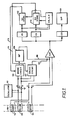
- an oscillator 101 drives an excitation coil 102 which is inductively coupled to detector coils 103, 104 connected in series and such that the E.M.F.s induced therein are in opposition.
- the arrangement of coils is disposed around the path of a conveyor belt shown in hatched outline 105 typically carrying foodstuffs, so that metallic impurities in the food can be detected.
- the signals developed in the excitation and detector coils are applied to a circuit via terminals A to E.
- the circuit is shown in block form in Fig. 1 and is shown in more detail in Fig. 2.
- the oscillatory signals applied by oscillator 101 to the terminals A and B are of a balanced anti-phase nature with reference to earth, a further terminal C being arranged to receive a screen connection.
- Input terminals D, E are arranged to receive the output of the series-connected detector coils 103, 104, including any residual drift voltage together with the detection signals.
- the oscillatory signal from terminals A and B is applied to first and second bridge circuits 106,107 the balances of which are adjustable by means of a feedback loop to be described later.
- An output is taken across a diagonal of each of the bridges, and the output from bridge 106 is fed through a 90° phase shifter circuit 108.
- first and second balancing signals which are of the same frequency as the signal from the oscillator 101, the balancing signals being in phase quadrature.
- balancing signals are combined with the output of the detection coils 103, 104 by combining means in the form of an operational amplifier IC10 and the amplitudes of the balancing signals are selected to cancel out any long term drifts in the output of the detector coils.
- the output of the amplifier IC10 is applied to three balanced demodulators which act as phase sensitive detectors, namely circuits IC1, IC2 and IC11.
- Circuit IC11 develops an output when metal is detected.
- the circuit is fed with a reference signal at the frequency of the oscillator 101 (by means not shown in Fig. 1).
- the phase of the reference signal is selected depending on the type of metal to be detected.
- the circuit IC11 thus develops a voltage level which increases when the balance of signals induced in the detector coils 103, 104 is disturbed by a metallic object on the conveyor belt.
- the output of IC11 is fed to output circuits 111 to be described in more detail hereinafter with reference to Fig. 2.
- the phase sensitive detectors IC1, IC2 are fed with reference signals that are respectively in phase and 90° out of phase with the signal from the oscillator 101.
- the voltage levels produced at the outputs of the circuits IC1, IC2 are stored by storage capacitor circuits 112, 113 and are representative of the out of balance condition of the phase quadrature components of the combined signal from IC10.
- the signals stored by circuits 112, 113 are fed back on paths 114, 115 to adjust the bridge circuits 106, 107 thereby to produce suitable magnitudes for the balancing signals on lines 109, 110, to balance out any long term drifts in the nominally zero output from the detector coils 103, 104.
- a circuit comprising IC5, IC6, IC13 is provided to control the manner in which the signals held in stores 112, 113 are updated when metal is detected. This is described in detail with reference to Fig.
- the store circuits are arranged to have a relatively short time constant at switch on of the circuit or after metal detection has occurred, in order to allow the system to balance itself quickly, and then it switches to a mode wherein the store circuits have a longer time constant, so that when metal is detected, the stored signal values held by circuits 112, 113 do not change rapidly so as to permit satisfactory detection of metal. Additionally a circuit is provided to prevent the store values being changed for a given time in response to metal detection, so as to hold the stored values in circuits 112,113 for a period corresponding to the expected time for the metal to move clear of the detector coils 103, 104, so that the system is automatically retained in its condition prior to detection of the metal.
- the signals from the oscillator on terminals A and B are passed through transistors TR1 and TR2 to a bridge circuit consisting of variable capacity diode pairs DD1 and DD2, and DD3 and DD4.
- DD1 and DD2 form a bridge circuit, the output of which goes to FET1; DD3 and DD4 from another bridge circuit, the output of which goes to FET2.
- the bridge circuits are in balance and no signal appears on the inputs of FET1 and FET2.
- the use of variable capacity diode bridges is a feature of the embodiment; this particular variable bridge element providing advantageous performance over other bridge elements which can be used as thermistors or FET's.
- the output on FET1 is phase-shifted by 90° at FET3 and the combined outputs from R26 and R37 are mixed at terminal 5 with the detector coil signal coming via R102 to the input of amplifier IC10, the detector coil signal having passed through a differential amplifier TR5, TR6, TR7 and emitter follower TRB.
- IC10 output which is on terminals 6 and 7, is passed to IC1, IC2 and IC11, each of which is a balanced demodulator which converts the input signals to a DC component proportional to the AC component that is in phase with a reference voltage fed to each demodulator.
- IC1 and IC2 therefore produce DC signals proportional to the in-phase and 90° components respectively of the outputs from FET1 and FET2.
- the respective signals from these two circuits are amplified via IC3 and IC4. These amplified signals are then fed to electronic switches IC5 and IC6 respectively.
- the first and third switches of IC5 and IC6 are normally switched on for a short period if the error in balance exceeds a certain amount.
- a threshold circuit IC13 which senses the outputs from IC3 and IC4 and determines whether they are higher or lower than an amount set by a chain of resistors R127, R128 and R129; the output from IC13 is fed via diodes D15 and D11 (via connections 14 and 15 respectively) to switch on the relevant circuits on IC5 and IC6.
- D15 controls IC4 which again controls the first switch of IC5 and IC6, whereas D11 controls the third switch of IC5 and IC6 after a time delay, this time delay being required and therefore arranged to allow for the passage of a piece of metal.
- an oscillator comprised of IC41 and its associated components causes capacitors C33 and C34 to be charged up to the output of IC3 and IC4 by switching on the first section of IC5 and IC6.
- the third switch of IC5 and IC6 is connected to resistors R69 and R70 respectively. The result of this is that a small charge from the capacitors C33 and C34 is transferred to capacitors C35 and C36 respectively.
- capacitors C35 and C36 are arranged to be substantially greater than C33 and C34, the ratios thereof being typically of the order of 100,000, the rate of change of the control voltage developed across C35 and C36 can be made extremely slow, not only by the ratio of the respective capacitors, but by the rate at which the oscillator section of IC41 is made to operate.
- initially D15 will effectively, by stopping the oscillator section of IC41, prevent any re-balance of the circuit until the time delay provided by IC13 output at D11 resets the balance. Normally this time delay is arranged to exceed the time that metal would be in the coil arrangement.
- the threshold detecting circuit IC13 is triggered to produce an output on line 14 which switches off the oscillator IC41.
- the first switch section is held on, so as to connect IC4 directly to C34.
- the third section of IC6 is off thus isolating C36 and holding its charge as the controlling voltage to be fed back to the bridge DD3, DD4.
- diode D11 After a timed delay an output is produced by IC13 via diode D11, which switches on the third section of IC6.
- oscillator IC41 starts to run and the system exbits a longer time constant as the charge on capacitor C36 follows more slowly the output at IC4.
- the oscillator IC41 is running, the first and third sections of IC6 are alternately switched thus transferring packets of charge from C34 to C36.
- This longer time constant can be adjusted by altering the rate of the oscillator and/or the relative capacities of C34 and C36.
- the actual detection part of the circuit comprises the demodulator IC11 which obtains a reference voltage via TR4 as mentioned above, the phase of which is controlled by a voltage applied to resistor R121.
- the input of the circuit including TR4 is shown as being derived from the junction of resistors R2 and R3, i.e. it is in phase with the signal applied to terminal B. It can alternatively be supplied 90° out of phase with this signal if required by, for example, taking the input to this circuit from the output capacitor C16 of FET4.
- a switching arrangement allows either input to be selected. This facility allows one to select the optimum mode of operation according to the product being examined and/or the most likely metal being sought.
- the output from the phase detector (or demodulator) IC11 passes through an amplifier IC12 and a voltage follower circuit IC14 to a trigger circuit consisting of IC16 which detects positive or negative excursions of IC12 output and provides signals indicative of these conditions on output terminals L, M.
- the last stage IC14 is capacitively coupled by C57 which eliminates the DC error from IC12. This is necessary because as the automatic balance circuits deviate over their control range, IC12 output will follow correspondingly, depending on whether its phase reference is similar to that of IC1 or IC2. In either event there will inevitably be some deviation from the normal and this will vary according to the drift error of the coil arrangement. The variation of output in IC12, however, will still occur when metal passes through the coil arrangement and will consist of a positive and negative pulse.
- Diodes D4 and D5 limit the input on C57 and prevent any excessive charge or discharge which would occur with a large piece of metal.
- the reference voltage for these diodes is obtained from the lower half of IC12.
- the charging resistor R130 for capacitor C56 is disconnected via switching circuit IC15 so that the reference voltage is held at its original value and does not follow the output of IC12 (top half) once it exceeds an amount sufficient to trigger IC16.
- resistor R134 is also disconnected via IC15 so that no charge is lost from capacitor C57 during the passage of a large piece of metal, whereas normally without these precautions considerable current would flow from R134 and the circuit would not restore to its original state unless the positive and negative charges caused by the passage of the piece of metal were exactly equal. This could only be the case if IC12 was accurately set to the middle of its output voltage range which, as previously stated, will not occur since it will tend to deviate with the degree of drift from the coil arrangement. It is possible, however, that once the circuit has triggered at IC16, R134 being disconnected, the circuit will take a very long time to restore because no charge can flow into C57.
- the output from the re-balance timer IC13 via D16 is arranged to switch a section of IC15 to short-circuit R134 until the circuit is re-balanced.
- the circuit as shown provides output signals on terminals L, M indicative of positive and negative excursions of IC12 output as described above.
- a piece of metal passing through the coil arrangement will therefore provide initially a signal of one polarity, then a signal of the opposite polarity at the output of IC12.
- Two signals are thereby provided at output terminals L, M which differ in timing by the time required for the metal to pass from between the first detector coil and excitation coil to between the second detector coil and excitation coil.
- This feature can be utilised to reject signals resulting from any occurrence other than the passage of metal through both detector coils of the coil arrangement.
- a circuit responsive only to presence of both output signals within a preset time span can be connected to terminals L, M in order to provide such a function.
- This may include two charging circuits, each being enabled by one of the two output signals to commence a charging or discharging operation. States of charge within preset limits may then be monitored for each circuit and a gating arrangement made responsive to both charging circuits being within these limits in order to provide an indication of a required detection.
- the rates of charge can be varied, e.g.
- variable resistance/ capacitance combination to set the time constant for each circuit, and the variation may be controlled in accordance with the speed of a conveyor belt passing samples through the coil arrangement.
- the expected time between output pulses on terminals L, M may advantageously be varied thereby according to the speed of the belt.
- the output from this circuit can then be used to provide an indication of detected metal and/or to operate a suitable rejection device for rejecting any contaminated samples.
- the circuit as described therefore provides operation with a time constant of variable length. This enables the circuit to cope with the various requirements, such as the ability to rebalance any residual drift and yet to detect adequately the passage of metal without commencing a rebalancing operation and thereby losing the immediately preceding state of balance.
Landscapes
- Life Sciences & Earth Sciences (AREA)
- Engineering & Computer Science (AREA)
- Physics & Mathematics (AREA)
- Remote Sensing (AREA)
- Geology (AREA)
- Environmental & Geological Engineering (AREA)
- Electromagnetism (AREA)
- General Life Sciences & Earth Sciences (AREA)
- General Physics & Mathematics (AREA)
- Geophysics (AREA)
- Geophysics And Detection Of Objects (AREA)
- Investigating Or Analyzing Materials By The Use Of Magnetic Means (AREA)
- Analysing Materials By The Use Of Radiation (AREA)
- Measurement Of Levels Of Liquids Or Fluent Solid Materials (AREA)
Claims (8)
Priority Applications (1)
| Application Number | Priority Date | Filing Date | Title |
|---|---|---|---|
| AT82300613T ATE23756T1 (de) | 1981-02-09 | 1982-02-08 | Metallsuchgeraet. |
Applications Claiming Priority (2)
| Application Number | Priority Date | Filing Date | Title |
|---|---|---|---|
| GB8103943 | 1981-02-09 | ||
| GB8103943 | 1981-02-09 |
Publications (3)
| Publication Number | Publication Date |
|---|---|
| EP0058076A2 EP0058076A2 (fr) | 1982-08-18 |
| EP0058076A3 EP0058076A3 (en) | 1982-08-25 |
| EP0058076B1 true EP0058076B1 (fr) | 1986-11-20 |
Family
ID=10519564
Family Applications (1)
| Application Number | Title | Priority Date | Filing Date |
|---|---|---|---|
| EP82300613A Expired EP0058076B1 (fr) | 1981-02-09 | 1982-02-08 | Appareil détecteur de métaux |
Country Status (6)
| Country | Link |
|---|---|
| US (2) | US4563645A (fr) |
| EP (1) | EP0058076B1 (fr) |
| JP (1) | JPS57189084A (fr) |
| AT (1) | ATE23756T1 (fr) |
| CA (1) | CA1194177A (fr) |
| DE (1) | DE3274391D1 (fr) |
Families Citing this family (49)
| Publication number | Priority date | Publication date | Assignee | Title |
|---|---|---|---|---|
| US4709213A (en) * | 1982-07-23 | 1987-11-24 | Garrett Electronics, Inc. | Metal detector having digital signal processing |
| GB2147706B (en) * | 1983-04-21 | 1987-02-04 | John Hugh Davey Walton | Apparatus for balancing an electrical network |
| US4613815A (en) * | 1983-04-27 | 1986-09-23 | Pall Corporation | Electromagnetic detector for metallic materials having an improved phase detection circuit |
| JPS6078378A (ja) * | 1983-10-05 | 1985-05-04 | Anritsu Corp | 金属検出装置 |
| GB8407009D0 (en) * | 1984-03-17 | 1984-04-18 | Parkway Instr Co Operative Ltd | Locating and detecting metal objects |
| GB2165650B (en) * | 1984-04-09 | 1988-04-27 | Dennis Amerena Parker | Method and apparatus for the quantative and qualitative measurement of small metal particles |
| GB8517257D0 (en) * | 1985-07-08 | 1985-08-14 | Goring Kerr Plc | Metal detector |
| US4959636A (en) * | 1987-12-17 | 1990-09-25 | Detection Systems Pty. Ltd. | Search head for metal detectors |
| WO1991004502A1 (fr) * | 1989-09-12 | 1991-04-04 | Bayliss Electronic Industries Pty. Ltd. | Detecteur de valeur minerale a champ induit |
| US5432444A (en) * | 1990-10-23 | 1995-07-11 | Kaisei Engineer Co., Ltd. | Inspection device having coaxial induction and exciting coils forming a unitary coil unit |
| EP0543648A1 (fr) * | 1991-11-21 | 1993-05-26 | Kaisei Engineer Co., Ltd. | Appareil et méthode pour l'inspection à l'induction électromagnétique |
| US5721489A (en) * | 1995-10-06 | 1998-02-24 | Garrett Electronics, Inc. | Metal detector method for identifying target size |
| US5691640A (en) * | 1995-11-17 | 1997-11-25 | Ramsey Technology, Inc. | Forced balance metal detector |
| US6407550B1 (en) | 1998-08-19 | 2002-06-18 | Metrotech Corporation | Line locator with accurate horizontal displacement detection |
| US6130539A (en) * | 1998-08-19 | 2000-10-10 | Metrotech Corporation | Automatic gain control for a line locator |
| US6268724B1 (en) | 1999-06-21 | 2001-07-31 | Quantum Magnetics | Device for selectively detecting metal objects |
| GB2361544B (en) * | 2000-04-20 | 2004-07-07 | Goring Kerr Ltd | Metal detector |
| GB0023303D0 (en) * | 2000-09-22 | 2000-11-08 | Safeline Ltd | Metal detector |
| RU2216028C2 (ru) * | 2000-11-20 | 2003-11-10 | Лубов Валерий Павлович | Металлоискатель |
| DE10122741A1 (de) * | 2001-05-10 | 2002-11-14 | Bosch Gmbh Robert | Detektor zur Ortung metallischer Gegenstände |
| US6803757B2 (en) | 2001-10-02 | 2004-10-12 | Bentley Nevada, Llc | Multi-coil eddy current proximity probe system |
| GB0201465D0 (en) * | 2002-01-23 | 2002-03-13 | Roke Manor Research | Pre-mri metal detector |
| FR2907223B1 (fr) * | 2006-10-13 | 2009-04-03 | Areva Np Sas | Procede et dispositif de detection d'anomalies structurelles dans une particule spherique,notamment dans une particule de combustible nucleaire pour reacteurs a haute temperature ou tres haute temperature. |
| RU2366982C2 (ru) * | 2006-11-20 | 2009-09-10 | Институт нефтегазовой геологии и геофизики им.А.А.Трофимука СО РАН (ИНГГ СО РАН) | Металлоискатель |
| US20080297158A1 (en) * | 2007-05-31 | 2008-12-04 | Zircon Corporation | Gradiometric Directional Metal Detector |
| US7893690B2 (en) * | 2007-07-19 | 2011-02-22 | Carnes Company, Inc. | Balancing circuit for a metal detector |
| EP2439560B1 (fr) * | 2010-10-07 | 2013-05-29 | Mettler-Toledo Safeline Limited | Procédé de fonctionnement d'un système de détection de métaux et système de détection de métaux |
| DE102010042512B4 (de) * | 2010-10-15 | 2025-07-24 | Ifm Electronic Gmbh | Induktiver Näherungsschalter mit verringerter Temperaturabhängigkeit |
| DE102010042511B4 (de) * | 2010-10-15 | 2025-07-24 | Ifm Electronic Gmbh | Induktiver Näherungsschalter mit verringerter Temperaturabhängigkeit |
| US9316537B2 (en) | 2011-06-29 | 2016-04-19 | Minesense Technologies Ltd. | Sorting materials using a pattern recognition, such as upgrading nickel laterite ores through electromagnetic sensor-based methods |
| US11219927B2 (en) | 2011-06-29 | 2022-01-11 | Minesense Technologies Ltd. | Sorting materials using pattern recognition, such as upgrading nickel laterite ores through electromagnetic sensor-based methods |
| AU2012277493B2 (en) | 2011-06-29 | 2017-04-27 | Minesense Technologies Ltd. | Extracting mined ore, minerals or other materials using sensor-based sorting |
| EP2544027A1 (fr) | 2011-07-08 | 2013-01-09 | Mettler-Toledo Safeline Limited | Détecteur de métaux pour les chaînes de production et de conditionnement |
| DE102011088406A1 (de) * | 2011-12-13 | 2013-06-13 | Robert Bosch Gmbh | Metallsensor |
| BR112014019417B1 (pt) | 2012-02-10 | 2022-06-28 | Illinois Tool Works Inc | Método de equilibrar um sinal de saída de um detector de metal de frequência variável e detector de metal |
| GB2499239B (en) * | 2012-02-10 | 2014-02-12 | Illinois Tool Works | Metal detector |
| AU2013201330B2 (en) * | 2012-03-06 | 2015-03-05 | Minelab Electronics Pty Limited | A method for detecting fast time constant targets using a metal detector |
| EP2844403B1 (fr) | 2012-05-01 | 2018-06-20 | Minesense Technologies Ltd. | Machine de tri de minéraux haute performance de type cascade |
| US9176597B2 (en) * | 2012-07-02 | 2015-11-03 | Stmicroelectronics Asia Pacific Pte Ltd | Directional capacitive proximity sensor with bootstrapping |
| US9236861B2 (en) | 2012-07-02 | 2016-01-12 | Stmicroelectronics Asia Pacific Pte Ltd | Capacitive proximity sensor with enabled touch detection |
| US9164629B2 (en) | 2012-08-06 | 2015-10-20 | Stmicroelectronics Asia Pacific Pte Ltd | Touch screen panel with slide feature |
| US9557390B2 (en) * | 2012-08-29 | 2017-01-31 | Minelab Electronics Pty Limited | Noise reduction circuitry for a metal detector |
| GB201302809D0 (en) * | 2013-02-18 | 2013-04-03 | Roke Manor Research | An object detector |
| US9454272B2 (en) | 2014-05-22 | 2016-09-27 | Stmicroelectronics Asia Pacific Pte Ltd | Touch screen for stylus emitting wireless signals |
| CN110090812B (zh) | 2014-07-21 | 2021-07-09 | 感矿科技有限公司 | 来自废物矿物的粗矿石矿物的高容量分离 |
| US9522415B2 (en) | 2014-07-21 | 2016-12-20 | Minesense Technologies Ltd. | Mining shovel with compositional sensors |
| EP3415902B1 (fr) * | 2017-06-14 | 2023-12-27 | Rolls-Royce Corporation | Système de profilage de contrainte résiduelle non destructif utilisant une détection inductive |
| AU2022390822A1 (en) | 2021-11-22 | 2024-07-04 | Minesense Technologies Ltd. | Compositional multispectral and hyperspectral imaging systems for mining shovels and associated methods |
| EP4394331B1 (fr) * | 2023-08-09 | 2025-04-16 | Melexis Technologies SA | Capteur d'angle inductif et capteur de couple inductif |
Family Cites Families (16)
| Publication number | Priority date | Publication date | Assignee | Title |
|---|---|---|---|---|
| US2744232A (en) * | 1952-03-06 | 1956-05-01 | Elbert N Shawhan | Magnetic and conducting materials detector |
| US2858505A (en) * | 1953-09-18 | 1958-10-28 | Sun Oil Co | Apparatus for the detection of foreign bodies |
| US2888026A (en) * | 1957-09-16 | 1959-05-26 | Reserve Mining Co | Automatic material proportioning system |
| US3573784A (en) * | 1968-10-02 | 1971-04-06 | Henry L Bachofer | Metal detecting apparatus for conveyor belt |
| US3614600A (en) * | 1969-07-31 | 1971-10-19 | Geonics Ltd | Electromagnetic prospecting apparatus for detecting electrically or magnetically responsive ore bodies |
| US3676772A (en) * | 1970-08-18 | 1972-07-11 | Nasa | Metallic intrusion detector system |
| GB1370233A (en) * | 1972-01-06 | 1974-10-16 | Goring Kerr Ltd | Electrical sorting apparatus |
| US3826973A (en) * | 1973-01-10 | 1974-07-30 | Benson R | Electromagnetic gradiometer |
| GB1490191A (en) * | 1975-01-16 | 1977-10-26 | Plessey Co Ltd | Metal detectors |
| US4006407A (en) * | 1975-03-10 | 1977-02-01 | Magnaflux Corporation | Non-destructive testing systems having automatic balance and sample and hold operational modes |
| US4099116A (en) * | 1977-01-17 | 1978-07-04 | Tyndall Jerry C | Metal detector with phase related circuit selective discrimination |
| JPS53114497A (en) * | 1977-02-17 | 1978-10-05 | Densoku Kougiyou Kk | Balanceeregulated circuit for metal detector |
| GB2025630B (en) * | 1977-11-10 | 1982-06-30 | Goring Kerr Ltd | Electrical bridge circuit with compensation for long-term drift |
| DE2825958C2 (de) * | 1978-06-14 | 1986-02-20 | Institut Dr. Friedrich Förster Prüfgerätebau GmbH & Co KG, 7410 Reutlingen | Magnetisches oder magnetinduktives Werkstoffprüfgerät mit Nullpunktkompensationseinrichtung |
| FR2443682A1 (fr) * | 1978-12-07 | 1980-07-04 | Commissariat Energie Atomique | Circuit de correction automatique d'un signal emis par un capteur differentiel desequilibre |
| US4300097A (en) * | 1979-07-27 | 1981-11-10 | Techna, Inc. | Induction balance metal detector with ferrous and non-ferrous metal identification |
-
1982
- 1982-02-08 AT AT82300613T patent/ATE23756T1/de not_active IP Right Cessation
- 1982-02-08 DE DE8282300613T patent/DE3274391D1/de not_active Expired
- 1982-02-08 EP EP82300613A patent/EP0058076B1/fr not_active Expired
- 1982-02-08 CA CA000395805A patent/CA1194177A/fr not_active Expired
- 1982-02-09 US US06/347,228 patent/US4563645A/en not_active Expired - Fee Related
- 1982-02-09 JP JP57019510A patent/JPS57189084A/ja active Pending
-
1985
- 1985-10-21 US US06/789,547 patent/US4659989A/en not_active Expired - Fee Related
Also Published As
| Publication number | Publication date |
|---|---|
| US4659989A (en) | 1987-04-21 |
| EP0058076A3 (en) | 1982-08-25 |
| JPS57189084A (en) | 1982-11-20 |
| EP0058076A2 (fr) | 1982-08-18 |
| CA1194177A (fr) | 1985-09-24 |
| DE3274391D1 (en) | 1987-01-08 |
| ATE23756T1 (de) | 1986-12-15 |
| US4563645A (en) | 1986-01-07 |
Similar Documents
| Publication | Publication Date | Title |
|---|---|---|
| US4563645A (en) | Inductively balanced oscillatory coil current for metal detection | |
| EP0196912B1 (fr) | Pont de mesure capacitif | |
| US4472676A (en) | Leakage impedance measuring system including a superimposed measuring voltage having a frequency differing slightly from system frequency | |
| US4414852A (en) | Automatic zero balance circuit | |
| US4240028A (en) | Means and method for determining water saturation of oil | |
| US6346812B1 (en) | Conditioner circuit for magnetic field sensor | |
| CA1164048A (fr) | Dispositif de surveillance pour le bloc de condensateurs d'un circuit de filtrage de courant continu | |
| JPS6232382A (ja) | 金属異物検知器 | |
| GB2025630A (en) | Electrical bridge circuit with compensation for long-term drift | |
| US3846688A (en) | Machine work sensor | |
| US4875007A (en) | Eddy current proximity system | |
| US5744968A (en) | Ratiometric circuit | |
| US4945336A (en) | Trouble detection apparatus for automobile air-bag system | |
| US3496453A (en) | Voltage sensing device | |
| JPS6341502B2 (fr) | ||
| US3493954A (en) | Object detection system | |
| US4038609A (en) | Replica bridge sensing circuit | |
| US4860839A (en) | Weighing apparatus including active low-pass filter means | |
| US4240047A (en) | Mechanical resonator oscillator having redundant parallel drive circuits | |
| GB2257524A (en) | Device for detecting defects in sensors | |
| JP3096788B2 (ja) | 金属検出装置 | |
| EP1065529B1 (fr) | Procédé et dispositif pour la détection des corps étrangers | |
| WO1995004256A1 (fr) | Capteur de deplacement capacitif | |
| SU894651A2 (ru) | Металлоискатель | |
| JP2633637B2 (ja) | 対称分保護リレー |
Legal Events
| Date | Code | Title | Description |
|---|---|---|---|
| PUAI | Public reference made under article 153(3) epc to a published international application that has entered the european phase |
Free format text: ORIGINAL CODE: 0009012 |
|
| PUAL | Search report despatched |
Free format text: ORIGINAL CODE: 0009013 |
|
| AK | Designated contracting states |
Designated state(s): AT BE CH DE FR GB IT LU NL SE |
|
| AK | Designated contracting states |
Designated state(s): AT BE CH DE FR GB IT LU NL SE |
|
| 17P | Request for examination filed |
Effective date: 19830203 |
|
| GRAA | (expected) grant |
Free format text: ORIGINAL CODE: 0009210 |
|
| AK | Designated contracting states |
Kind code of ref document: B1 Designated state(s): AT BE CH DE FR GB IT LI LU NL SE |
|
| REF | Corresponds to: |
Ref document number: 23756 Country of ref document: AT Date of ref document: 19861215 Kind code of ref document: T |
|
| ITF | It: translation for a ep patent filed | ||
| REF | Corresponds to: |
Ref document number: 3274391 Country of ref document: DE Date of ref document: 19870108 |
|
| ET | Fr: translation filed | ||
| PLBE | No opposition filed within time limit |
Free format text: ORIGINAL CODE: 0009261 |
|
| STAA | Information on the status of an ep patent application or granted ep patent |
Free format text: STATUS: NO OPPOSITION FILED WITHIN TIME LIMIT |
|
| 26N | No opposition filed | ||
| ITTA | It: last paid annual fee | ||
| PGFP | Annual fee paid to national office [announced via postgrant information from national office to epo] |
Ref country code: NL Payment date: 19910228 Year of fee payment: 10 |
|
| PGFP | Annual fee paid to national office [announced via postgrant information from national office to epo] |
Ref country code: GB Payment date: 19910514 Year of fee payment: 10 |
|
| PGFP | Annual fee paid to national office [announced via postgrant information from national office to epo] |
Ref country code: DE Payment date: 19910722 Year of fee payment: 10 Ref country code: AT Payment date: 19910722 Year of fee payment: 10 |
|
| PGFP | Annual fee paid to national office [announced via postgrant information from national office to epo] |
Ref country code: FR Payment date: 19910723 Year of fee payment: 10 Ref country code: CH Payment date: 19910723 Year of fee payment: 10 Ref country code: BE Payment date: 19910723 Year of fee payment: 10 |
|
| PGFP | Annual fee paid to national office [announced via postgrant information from national office to epo] |
Ref country code: SE Payment date: 19910725 Year of fee payment: 10 Ref country code: LU Payment date: 19910725 Year of fee payment: 10 |
|
| EPTA | Lu: last paid annual fee | ||
| PG25 | Lapsed in a contracting state [announced via postgrant information from national office to epo] |
Ref country code: LU Free format text: LAPSE BECAUSE OF NON-PAYMENT OF DUE FEES Effective date: 19920208 Ref country code: GB Effective date: 19920208 Ref country code: AT Effective date: 19920208 |
|
| PG25 | Lapsed in a contracting state [announced via postgrant information from national office to epo] |
Ref country code: SE Effective date: 19920209 |
|
| PG25 | Lapsed in a contracting state [announced via postgrant information from national office to epo] |
Ref country code: BE Effective date: 19920228 |
|
| PG25 | Lapsed in a contracting state [announced via postgrant information from national office to epo] |
Ref country code: LI Effective date: 19920229 Ref country code: CH Effective date: 19920229 |
|
| BERE | Be: lapsed |
Owner name: GORING KERR LTD Effective date: 19920228 |
|
| PG25 | Lapsed in a contracting state [announced via postgrant information from national office to epo] |
Ref country code: NL Effective date: 19920901 |
|
| GBPC | Gb: european patent ceased through non-payment of renewal fee | ||
| NLV4 | Nl: lapsed or anulled due to non-payment of the annual fee | ||
| PG25 | Lapsed in a contracting state [announced via postgrant information from national office to epo] |
Ref country code: FR Effective date: 19921030 |
|
| REG | Reference to a national code |
Ref country code: CH Ref legal event code: PL |
|
| PG25 | Lapsed in a contracting state [announced via postgrant information from national office to epo] |
Ref country code: DE Effective date: 19921103 |
|
| REG | Reference to a national code |
Ref country code: FR Ref legal event code: ST |
|
| EUG | Se: european patent has lapsed |
Ref document number: 82300613.5 Effective date: 19920904 |