EP0058852B1 - Dispositif à semiconducteur à cadre de connexion découpé d'une tôle - Google Patents
Dispositif à semiconducteur à cadre de connexion découpé d'une tôle Download PDFInfo
- Publication number
- EP0058852B1 EP0058852B1 EP82100766A EP82100766A EP0058852B1 EP 0058852 B1 EP0058852 B1 EP 0058852B1 EP 82100766 A EP82100766 A EP 82100766A EP 82100766 A EP82100766 A EP 82100766A EP 0058852 B1 EP0058852 B1 EP 0058852B1
- Authority
- EP
- European Patent Office
- Prior art keywords
- semiconductor
- sheet metal
- arrangement
- semiconductor device
- semiconductor body
- Prior art date
- Legal status (The legal status is an assumption and is not a legal conclusion. Google has not performed a legal analysis and makes no representation as to the accuracy of the status listed.)
- Expired
Links
Images
Classifications
-
- H—ELECTRICITY
- H10—SEMICONDUCTOR DEVICES; ELECTRIC SOLID-STATE DEVICES NOT OTHERWISE PROVIDED FOR
- H10W—GENERIC PACKAGES, INTERCONNECTIONS, CONNECTORS OR OTHER CONSTRUCTIONAL DETAILS OF DEVICES COVERED BY CLASS H10
- H10W90/00—Package configurations
- H10W90/811—Multiple chips on leadframes
-
- H—ELECTRICITY
- H10—SEMICONDUCTOR DEVICES; ELECTRIC SOLID-STATE DEVICES NOT OTHERWISE PROVIDED FOR
- H10W—GENERIC PACKAGES, INTERCONNECTIONS, CONNECTORS OR OTHER CONSTRUCTIONAL DETAILS OF DEVICES COVERED BY CLASS H10
- H10W72/00—Interconnections or connectors in packages
-
- H—ELECTRICITY
- H10—SEMICONDUCTOR DEVICES; ELECTRIC SOLID-STATE DEVICES NOT OTHERWISE PROVIDED FOR
- H10W—GENERIC PACKAGES, INTERCONNECTIONS, CONNECTORS OR OTHER CONSTRUCTIONAL DETAILS OF DEVICES COVERED BY CLASS H10
- H10W72/00—Interconnections or connectors in packages
- H10W72/071—Connecting or disconnecting
- H10W72/075—Connecting or disconnecting of bond wires
- H10W72/07521—Aligning
-
- H—ELECTRICITY
- H10—SEMICONDUCTOR DEVICES; ELECTRIC SOLID-STATE DEVICES NOT OTHERWISE PROVIDED FOR
- H10W—GENERIC PACKAGES, INTERCONNECTIONS, CONNECTORS OR OTHER CONSTRUCTIONAL DETAILS OF DEVICES COVERED BY CLASS H10
- H10W72/00—Interconnections or connectors in packages
- H10W72/50—Bond wires
- H10W72/541—Dispositions of bond wires
- H10W72/5445—Dispositions of bond wires being orthogonal to a side surface of the chip, e.g. parallel arrangements
-
- H—ELECTRICITY
- H10—SEMICONDUCTOR DEVICES; ELECTRIC SOLID-STATE DEVICES NOT OTHERWISE PROVIDED FOR
- H10W—GENERIC PACKAGES, INTERCONNECTIONS, CONNECTORS OR OTHER CONSTRUCTIONAL DETAILS OF DEVICES COVERED BY CLASS H10
- H10W90/00—Package configurations
- H10W90/701—Package configurations characterised by the relative positions of pads or connectors relative to package parts
- H10W90/751—Package configurations characterised by the relative positions of pads or connectors relative to package parts of bond wires
- H10W90/756—Package configurations characterised by the relative positions of pads or connectors relative to package parts of bond wires between a chip and a stacked lead frame, conducting package substrate or heat sink
-
- Y—GENERAL TAGGING OF NEW TECHNOLOGICAL DEVELOPMENTS; GENERAL TAGGING OF CROSS-SECTIONAL TECHNOLOGIES SPANNING OVER SEVERAL SECTIONS OF THE IPC; TECHNICAL SUBJECTS COVERED BY FORMER USPC CROSS-REFERENCE ART COLLECTIONS [XRACs] AND DIGESTS
- Y10—TECHNICAL SUBJECTS COVERED BY FORMER USPC
- Y10S—TECHNICAL SUBJECTS COVERED BY FORMER USPC CROSS-REFERENCE ART COLLECTIONS [XRACs] AND DIGESTS
- Y10S257/00—Active solid-state devices, e.g. transistors, solid-state diodes
- Y10S257/909—Macrocell arrays, e.g. gate arrays with variable size or configuration of cells
Definitions
- the invention relates to a semiconductor arrangement with connecting conductors cut out of sheet metal and having main surfaces, with contact surfaces for the attachment of support points provided for each bonding wire and with bond wires arranged in alignment one behind the other, which are fastened on the one hand to a semiconductor body seated on one of the contact surfaces and on the other hand to a support point.
- the invention aims to improve such an arrangement in such a way that a reversal of the direction of movement of the bonder becomes superfluous.
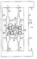
- the invention is explained in more detail using an exemplary embodiment in conjunction with the single figure.
- the figure shows a top view of an unencapsulated semiconductor arrangement.
- a full-wave rectifier bridge is shown in the figure.
- This has a conductor system 15 cut out of sheet metal, which contains two longitudinal webs 16, 17 and two transverse webs 18, 19 and two sealing webs 20, 25.
- the bridge has four connecting conductors 21, 22, 23 and 24, which are connected to the longitudinal webs 16 and 17, respectively.
- the conductor system has main surfaces, one of which is presented to the viewer and cut surfaces that are perpendicular to the main surfaces.
- the connection conductor 21 has at one end a contact surface 26 on which a semiconductor body 35 is seated. It also has a base 31 for attaching a bonding wire 39.
- the connecting conductor 22 carries a contact surface 27 on which a semiconductor body 36 is seated and a support point 32 for a bonding wire 40.
- the connecting conductor 23 has two support points 29, 30 for two bonding wires 37, 38.
- the connecting conductor 24 has a contact surface 28 which is suitable for the inclusion of two semiconductor bodies 33 and 34 is determined.
- the semiconductor bodies are arranged one behind the other in two adjacent groups. However, this is not mandatory, for certain purposes, e.g. For a center point circuit, it may also be sufficient if only two semiconductor bodies lying one behind the other are provided.
- the contact surfaces belonging to the semiconductor bodies 35 and 33 and their supporting points lie one behind the other, as seen in the feed direction (arrow direction).
- the bond wires 37 and 39 can thus be arranged in alignment one behind the other.
- a bond connection on the semiconductor body is always followed by a bond connection, so that the bonder only has to be moved in one direction. This leads to a considerable acceleration of the bonding.
- the same also applies to the semiconductor bodies 34 and 36 and the support points 32, 30 assigned to them.
- the contact surfaces and support points are cranked one or more times as seen from the main surfaces of the conductor system 15. This is recommended for optimal use of space if a fixed distance between the connection conductors 21 and 22 or 23 and 24 is prescribed. If the distance mentioned is freely selectable, the support points and contact areas can be formed as straight strips.
- the semiconductor bodies can be soldered or glued to the connection conductors with their contact surfaces. This means that they are mechanically supported and electrically contacted.
- the semiconductor arrangement is e.g. encapsulated with plastic.
- the connecting conductors and the sealing webs are then cut off at the dashed points.
Landscapes
- Wire Bonding (AREA)
Claims (2)
Applications Claiming Priority (2)
| Application Number | Priority Date | Filing Date | Title |
|---|---|---|---|
| DE3106376 | 1981-02-20 | ||
| DE19813106376 DE3106376A1 (de) | 1981-02-20 | 1981-02-20 | Halbleiteranordnung mit aus blech ausgeschnittenen anschlussleitern |
Publications (3)
| Publication Number | Publication Date |
|---|---|
| EP0058852A2 EP0058852A2 (fr) | 1982-09-01 |
| EP0058852A3 EP0058852A3 (en) | 1983-06-01 |
| EP0058852B1 true EP0058852B1 (fr) | 1987-06-03 |
Family
ID=6125375
Family Applications (1)
| Application Number | Title | Priority Date | Filing Date |
|---|---|---|---|
| EP82100766A Expired EP0058852B1 (fr) | 1981-02-20 | 1982-02-03 | Dispositif à semiconducteur à cadre de connexion découpé d'une tôle |
Country Status (4)
| Country | Link |
|---|---|
| US (1) | US4532538A (fr) |
| EP (1) | EP0058852B1 (fr) |
| JP (1) | JPS57153442A (fr) |
| DE (2) | DE3106376A1 (fr) |
Families Citing this family (15)
| Publication number | Priority date | Publication date | Assignee | Title |
|---|---|---|---|---|
| IT1212708B (it) * | 1983-02-28 | 1989-11-30 | Ates Componenti Elettron | Dispositivo di potenza a semiconduttore costituito da una molteplicita' di elementi attivi uguali collegati in parallelo. |
| FR2571895B1 (fr) * | 1984-10-16 | 1987-07-24 | Silicium Semiconducteur Ssc | Procede de montage de deux composants semi-conducteurs dans un boitier commun et dispositif obtenu par ce procede |
| JPS61269345A (ja) * | 1985-05-24 | 1986-11-28 | Hitachi Ltd | 半導体装置 |
| JPS62142850U (fr) * | 1986-03-04 | 1987-09-09 | ||
| JPH0740790B2 (ja) * | 1987-02-23 | 1995-05-01 | 株式会社東芝 | 大電力パワ−モジユ−ル |
| IT1221585B (it) * | 1987-05-18 | 1990-07-12 | S G S Microelettronica Spa Ora | Circuito modulare a piu' piastrine a semiconduttore in capsulato in resina,e relativo procedimento di fabbrivazione |
| FR2617636A1 (fr) * | 1987-07-02 | 1989-01-06 | Neiman Sa | Procede de fabrication d'un composant electronique de puissance et composants obtenus par ce procede |
| US5084753A (en) * | 1989-01-23 | 1992-01-28 | Analog Devices, Inc. | Packaging for multiple chips on a single leadframe |
| US4979017A (en) * | 1989-02-23 | 1990-12-18 | Adam Mii | Semiconductor element string structure |
| US4916519A (en) * | 1989-05-30 | 1990-04-10 | International Business Machines Corporation | Semiconductor package |
| JP2519806B2 (ja) * | 1989-09-12 | 1996-07-31 | 株式会社東芝 | 樹脂封止型半導体装置 |
| JPH03128936U (fr) * | 1990-12-27 | 1991-12-25 | ||
| JP3096824B2 (ja) * | 1992-04-17 | 2000-10-10 | ローム株式会社 | Led製造用フレームおよびこれを用いたledの製造方法 |
| EP0696818B1 (fr) * | 1994-08-12 | 2004-07-07 | Infineon Technologies AG | Dispositif semi-conducteur avec boítier isolant |
| US6329714B1 (en) | 1999-11-01 | 2001-12-11 | General Semiconductor, Inc. | Hybrid S.C. devices and method of manufacture thereof |
Family Cites Families (15)
| Publication number | Priority date | Publication date | Assignee | Title |
|---|---|---|---|---|
| US3461549A (en) * | 1966-03-09 | 1969-08-19 | Matsushita Electronics Corp | Method for manufacturing semiconductor devices |
| NL6604965A (fr) * | 1966-04-14 | 1967-10-16 | ||
| GB1196452A (en) * | 1967-01-19 | 1970-06-24 | Lucas Industries Ltd | Semiconductor Circuits |
| DE1614491A1 (de) * | 1967-04-08 | 1970-02-26 | Siemens Ag | Halbleiterbauelement |
| US3490141A (en) * | 1967-10-02 | 1970-01-20 | Motorola Inc | High voltage rectifier stack and method for making same |
| JPS553815B1 (fr) * | 1967-10-02 | 1980-01-26 | ||
| BE755950A (fr) * | 1969-09-11 | 1971-03-09 | Philips Nv | Procede permettant d'etablir des liaisons electriques entre desemplacements de contact d'un corps semiconducteur et des conducteurs d'alimentation |
| US3619734A (en) * | 1969-12-17 | 1971-11-09 | Rca Corp | Assembly of series connected semiconductor elements having good heat dissipation |
| NL7108092A (fr) * | 1970-06-18 | 1971-12-21 | ||
| DE2146558C3 (de) * | 1971-09-17 | 1979-09-06 | Siemens Ag, 1000 Berlin Und 8000 Muenchen | Anordnung der Stromschienen in einer Gleichrichteranlage |
| JPS5548700B2 (fr) * | 1973-01-30 | 1980-12-08 | ||
| JPS5272170A (en) * | 1975-12-12 | 1977-06-16 | Nec Corp | Package for semiconductor elements |
| US4142203A (en) * | 1976-12-20 | 1979-02-27 | Avx Corporation | Method of assembling a hermetically sealed semiconductor unit |
| JPS555650A (en) * | 1978-06-30 | 1980-01-16 | Asahi Transformer | Blood vessel negative pressure wave amplifying system |
| JPS604991B2 (ja) * | 1979-05-11 | 1985-02-07 | 株式会社東芝 | ディスプレイ装置 |
-
1981
- 1981-02-20 DE DE19813106376 patent/DE3106376A1/de not_active Withdrawn
-
1982
- 1982-02-03 DE DE8282100766T patent/DE3276511D1/de not_active Expired
- 1982-02-03 EP EP82100766A patent/EP0058852B1/fr not_active Expired
- 1982-02-08 US US06/347,030 patent/US4532538A/en not_active Expired - Fee Related
- 1982-02-17 JP JP57024282A patent/JPS57153442A/ja active Pending
Also Published As
| Publication number | Publication date |
|---|---|
| JPS57153442A (en) | 1982-09-22 |
| EP0058852A3 (en) | 1983-06-01 |
| DE3106376A1 (de) | 1982-09-09 |
| US4532538A (en) | 1985-07-30 |
| EP0058852A2 (fr) | 1982-09-01 |
| DE3276511D1 (en) | 1987-07-09 |
Similar Documents
| Publication | Publication Date | Title |
|---|---|---|
| EP0058852B1 (fr) | Dispositif à semiconducteur à cadre de connexion découpé d'une tôle | |
| DE69621851T2 (de) | Mehrchipanlage und sandwich-typ verfahren zur herstellung durch verwendung von leitern | |
| DE3414961C2 (fr) | ||
| DE10310809B4 (de) | Leistungshalbleitereinrichtung | |
| DE69211821T2 (de) | Innere Leiterstruktur einer Halbleiteranordnung | |
| DE68917798T2 (de) | Anschlussstruktur und Verfahren zu deren Herstellung. | |
| DE69205078T2 (de) | Verbindungstechnik für elektronische Vorrichtungen. | |
| DE69004581T2 (de) | Plastikumhüllte Hybrid-Halbleiteranordnung. | |
| DE3810899C2 (fr) | ||
| DE10105086B4 (de) | Leistungsmodul | |
| DE69313062T2 (de) | Chip-Direktmontage | |
| DE2806099A1 (de) | Halbleiter-baugruppe | |
| DE10119502B4 (de) | Halbleitergerät mit gleichmäßigen Strompfaden und kleinem Aufbau | |
| DE102004045896B4 (de) | Transponder mit Antenne und Flip-Chip-Modul und Verfahren zu dessen Herstellung | |
| DE10251527B4 (de) | Verfahren zur Herstellung einer Stapelanordnung eines Speichermoduls | |
| DE3243689C2 (fr) | ||
| EP0696818B1 (fr) | Dispositif semi-conducteur avec boítier isolant | |
| DE3930858C2 (de) | Modulaufbau | |
| DE3323463A1 (de) | Tastenschalter | |
| DE3619636A1 (de) | Gehaeuse fuer integrierte schaltkreise | |
| EP0776041B1 (fr) | Module semi-conducteur de puissance | |
| DE4333956A1 (de) | Verfahren zur Anbringung von integrierten Schaltungschips mit TAB-Struktur auf ein Substrat | |
| DE3628556C1 (en) | Semiconductor device | |
| EP0278484A2 (fr) | Méthode de fabrication d'une plaquette utilisée pour la digitalisation | |
| EP1576703B1 (fr) | Faisceau de cables plats |
Legal Events
| Date | Code | Title | Description |
|---|---|---|---|
| PUAI | Public reference made under article 153(3) epc to a published international application that has entered the european phase |
Free format text: ORIGINAL CODE: 0009012 |
|
| AK | Designated contracting states |
Designated state(s): DE FR GB IT |
|
| PUAL | Search report despatched |
Free format text: ORIGINAL CODE: 0009013 |
|
| AK | Designated contracting states |
Designated state(s): DE FR GB IT |
|
| 17P | Request for examination filed |
Effective date: 19830629 |
|
| GRAA | (expected) grant |
Free format text: ORIGINAL CODE: 0009210 |
|
| AK | Designated contracting states |
Kind code of ref document: B1 Designated state(s): DE FR GB IT |
|
| PG25 | Lapsed in a contracting state [announced via postgrant information from national office to epo] |
Ref country code: IT Free format text: LAPSE BECAUSE OF FAILURE TO SUBMIT A TRANSLATION OF THE DESCRIPTION OR TO PAY THE FEE WITHIN THE PRESCRIBED TIME-LIMIT;WARNING: LAPSES OF ITALIAN PATENTS WITH EFFECTIVE DATE BEFORE 2007 MAY HAVE OCCURRED AT ANY TIME BEFORE 2007. THE CORRECT EFFECTIVE DATE MAY BE DIFFERENT FROM THE ONE RECORDED. Effective date: 19870603 |
|
| REF | Corresponds to: |
Ref document number: 3276511 Country of ref document: DE Date of ref document: 19870709 |
|
| ET | Fr: translation filed | ||
| PLBE | No opposition filed within time limit |
Free format text: ORIGINAL CODE: 0009261 |
|
| STAA | Information on the status of an ep patent application or granted ep patent |
Free format text: STATUS: NO OPPOSITION FILED WITHIN TIME LIMIT |
|
| 26N | No opposition filed | ||
| PG25 | Lapsed in a contracting state [announced via postgrant information from national office to epo] |
Ref country code: FR Free format text: LAPSE BECAUSE OF NON-PAYMENT OF DUE FEES Effective date: 19881028 |
|
| PG25 | Lapsed in a contracting state [announced via postgrant information from national office to epo] |
Ref country code: DE Effective date: 19881101 |
|
| GBPC | Gb: european patent ceased through non-payment of renewal fee | ||
| PG25 | Lapsed in a contracting state [announced via postgrant information from national office to epo] |
Ref country code: GB Free format text: LAPSE BECAUSE OF NON-PAYMENT OF DUE FEES Effective date: 19881121 |
|
| REG | Reference to a national code |
Ref country code: FR Ref legal event code: ST |