EP0058997A1 - Digitale Verarbeitungsschaltung mit Multiplizierfunktion - Google Patents
Digitale Verarbeitungsschaltung mit Multiplizierfunktion Download PDFInfo
- Publication number
- EP0058997A1 EP0058997A1 EP82101443A EP82101443A EP0058997A1 EP 0058997 A1 EP0058997 A1 EP 0058997A1 EP 82101443 A EP82101443 A EP 82101443A EP 82101443 A EP82101443 A EP 82101443A EP 0058997 A1 EP0058997 A1 EP 0058997A1
- Authority
- EP
- European Patent Office
- Prior art keywords
- circuit
- multiplier
- booth
- input
- partial
- Prior art date
- Legal status (The legal status is an assumption and is not a legal conclusion. Google has not performed a legal analysis and makes no representation as to the accuracy of the status listed.)
- Granted
Links
Images


Classifications
-
- G—PHYSICS
- G06—COMPUTING OR CALCULATING; COUNTING
- G06F—ELECTRIC DIGITAL DATA PROCESSING
- G06F7/00—Methods or arrangements for processing data by operating upon the order or content of the data handled
- G06F7/38—Methods or arrangements for performing computations using exclusively denominational number representation, e.g. using binary, ternary, decimal representation
- G06F7/48—Methods or arrangements for performing computations using exclusively denominational number representation, e.g. using binary, ternary, decimal representation using non-contact-making devices, e.g. tube, solid state device; using unspecified devices
- G06F7/52—Multiplying; Dividing
- G06F7/523—Multiplying only
- G06F7/527—Multiplying only in serial-parallel fashion, i.e. one operand being entered serially and the other in parallel
- G06F7/5272—Multiplying only in serial-parallel fashion, i.e. one operand being entered serially and the other in parallel with row wise addition of partial products
-
- G—PHYSICS
- G10—MUSICAL INSTRUMENTS; ACOUSTICS
- G10L—SPEECH ANALYSIS TECHNIQUES OR SPEECH SYNTHESIS; SPEECH RECOGNITION; SPEECH OR VOICE PROCESSING TECHNIQUES; SPEECH OR AUDIO CODING OR DECODING
- G10L19/00—Speech or audio signals analysis-synthesis techniques for redundancy reduction, e.g. in vocoders; Coding or decoding of speech or audio signals, using source filter models or psychoacoustic analysis
Definitions
- the present invention relates to a digital processing circuit, and more particularly to a digital circuit with a multiplication function making use of the Booth's algorithm.
- an easy algorithm is employed in the case of multiplying a multiplicand X by a multiplier Y, that is, partial products equal to the number of bits in the multiplier Y are produced -by executing multiplications of the multiplicand X by the respective bits in the multiplier Y, and they are added each other, thereby the result is obtained.
- N partial products are produced for an N-bit multiplier Y, and N times of addition are necessitated to obtain the result.
- a correction circuit for a sign processing is also necessitated. Therefore, a great many hardware elements have to be included in the LSI circuit of this algorithm. It was not so valuable in view of practical use.
- the Booth's algorithm is useful. This is an algorithm in which a multiplier and a multiplicand represented in a complement form are multiplied by each other. According to this algorithm, a number of partial products is reduced to one-half of the above-described general case (N/2) and a sign processing is also executed simultaneously in the process of producing partial products, so that this is favorable for a high speed processing.
- N/2 general case
- a hardware for executing the Booth's algorithm becomes very complex. Expecially, many circuit elements for producing partial products and for adding the produced partial products are necessitated. Furthermore, the combination of these circuits are complexed and hence the manufacture of the LSI circuit is difficult.
- Another object of the present invention is to provide a digital processing circuit having multiplier function that is suitable for processing signals in a low frequency band such as speeches.
- Still another object of the present invention is to provide a digital circuit for executing a multiplication operation on the basis of the Booth's algorithm with a small number of circuit elements.
- Yet another object of the present invention is to provide a digital circuit in which data input/output can be controlled by a fewer kinds of timing signals (clock signals).
- a still further object of the present invention is to provide a multiplier circuit in which a decode processing, a partial product producing processing and a partial product adding processing based on the Booth's algorithm are executed within a same cycle.
- a digital processing circuit comprises first means for storing a multiplicand, second means for storing a multiplier, third means for producing coefficients by decoding the multiplier read out of the second means according to the Booth's algorithm, fourth means coupled to the third means and the first means for producing patial products by multiplying the multiplicand by the coefficients, fifth means having first and second input sections for executing addition of first and second inputs received at the first input section and at the second input section, respectively, the first input section being coupled to the fourth means and receiving the partial products as the first input, sixth means for receiving a result of addition from the fifth means and feeding back the result to the second section of the fifth means as second input of the fifth means and seventh means coupled to said fifth or sixth means for outputting a result of multiplication.
- the fourth means is required only to multiply the multiplicand input thereto from the first means by the coefficients produced according to the Booth's algorithm to produce partial products and to merely transfer the results of multiplication to the fifth means.
- the fifth means and the sixth means are coupled in a ring shape so as to form a loop. Accordingly, by circulating data with the aid of this loop, accumulation of the partial products can be achieved and eventually the result of multiplication can be obtained.
- a multiplication operation based on the Booth's algorithm can be executed by means of simple hardware elements (the first to sixth.means) without providing many partial product producing circuits and many adder circuits.
- timing control if provision is made such that at least the output timing of the fourth means for producing partial products and the input timing of the fifth means for adding the partial products may be maintained in a synchronized-relation, then erroneous operations can be prevented without strictly controlling input and output timings for each of the respective partial product producing circuits and the respective adder circuits as is the case with the multiplier circuit in the prior art. Accordingly, timing control is extremely easy.
- the coefficient producing circuit (the third means) also could be provided only one. Accordingly, a further reduced number of hardware elements as compared to the prior art circuit can suffice.
- the input and output of the third means may take a parallel form, it becomes possible to process the production of coefficients, production of partial products and addition of partial products in the same cycle, and this is effective both for timing control and for circuit design. Especially, with regard to clock frequencies for timing control, only one kind of frequency is sufficient.
- the heretofore well known multiplication algorithm is such that partial products of a multiplicand X by respective bits of a multiplier Y are produced respectively and then they are all added together as shown in Fig. 1. It is clean that for a multiplier of N bit, N partial products would be produced. In order to obtain a resultant product P, N times of addition were necessitated, and hence this algorithm was not suitable for a multiplier circuit which was required to have an increased operation speed. Therefore, various multiplication algorithms have been investigated, and among them, for instance, the 2-bit Booth's algorithm has been proved to be especially suitable for formation of a multiplier circuit in an LSI technical field.
- the 2-bit Booth's algorithm means an algorithm in which two numbers represented in the form of complements on two are multiplied by each other. Now this algorithm will be explained assuming that a multiplicand is X and a multiplier is Y.
- the multiplicand X is represented in the form of a complement on two, as follows; where x n is '0' when the multiplicand X is a positive number while it is '1' when the multiplicand X is a negative number, and in the case of a negative number, xi represents the respective bits obtained by inverting the respective bits in the binary code representing the original number and adding one to the least significant bit.
- Equation-(2) can be modified as follows:
- Equation-(3) the product of X and Y is represented as follows: where each term on the right side (-2y 2i+2 + Y 2i+1 + Y 2i ) x. 2 2i forms the partial product.
- n/2 partial products are obtained, in which 2 2i represents the weight of each bit.
- a partial product can be produced in the form containing a sign bit without specially dealing with a sign bit in the form of a complement on two, and therefore, there is provided an advantage with respect to hardwares that a correction circuit for sign operation is not necessitated.
- FIG. 2 One construction of a heretofore known parallel multiplier circuit for, executing the Booth's algorithm is illustrated in Fig. 2.
- This figure shows the case where two 4-digit numbers are multiplied, and x 1 x 2 x 3 x 4 represents a multiplicant, while y 1 y 2 y 3 y 4 represents a multiplier.
- a partial product is produced by a partial product producing circuit 2a.
- Addition of the output of this circuit 2a to a partial sum of partial products is executed by a full adder 3a.
- a similar operation is executed for three consecutive bits y 2 , y 3 and y 4 in the other Booth's decoder, and the corresponding partial product is produced by a partial product producing circuit 5a.
- the less significant two bits of the partial product is added to the more significant two bits of the output from the preceding full adder 3a by another full adder 6a.
- a carry is also output, if exists.
- additions for the respective corresponding bits are executed by a full adder 7a, and thereby a product (P 1 P 2 P 3 .... P 7 ) is obtained.
- An additional bit P 8 is a sign bit for the product.
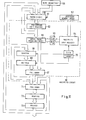
- FIG. 3 A block diagram of a digital processing circuit with multiplier function according to one preferred embodiment of the present invention in which the above-mentioned shortcomings in hardwares and timing control are eliminated, is illustrated in Fig. 3.
- this circuit there are provided only one full adder 5 and one partial product producing circuit 4 which are operated under the Booth's algorithm. It is intended to obtain a product by repeating an operation of adding a partial product produced by the partial product producing circuit 4 to a total sum of the previously obtained partial products by the full adder 5.
- a multiplicand is set in a register 1 and a multiplier is set in a shift register 2.
- the multiplier which is set in the shift register 2 with the least significant digit located at the left end bit portion, is shifted bit by bit as synchronized with a clock issued from a clock generator circuit 8 (in particular, this could be a clock generator used within a speech processing system), and at first the least significant three bits are input to a Booth's decoder 3.
- the output of the decoder 3 obtained by decoding the input three bits according to Table- above is input to the partial product producing circuit 4 joinlly with the multiplicand.
- a partial product produced by the partial product producing circuit 4 is input to the full adder 5 coupled to output of a register 7 which holds a sum (partial sum) of the previously obtained partial products, and a new partial sum is produced in this full adder 5 and is input to a shift register 6 .
- This shift register 6 is inserted for the purpose of transferring the output of the full adder 5 to the register 7 which holds the partial sum at a predetermined timing in response to a clock applied from a clock frequency-divider circuit 9.
- a clock for driving the register 7 is also applied from the same clock frequency-divider circuit 9 and hence it is synchronized with the clock applied to the shift register 6.
- the Booth's decoder 3 executes a decode processing for three consecutive bits in the multiplier, and transfers the decoded output to the partial product producing circuit 4.
- This circuit 4 carries out multiplication of the multiplicand by a decoded output to produce a partial product each time when a decoded output is transferred. These operation timings can be easily controlled so as to synchronize with another circuit by means of the same clock generator. Further, all the partial products necessitated in multiplication are produced by the single partial product producing circuit 4.
- the full adder 5, shift register 6 and register 7 are coupled in a loop, and hence, addition (production of a partial sum) is effected once within each partial product producing cycle. According, production of a partial sum is effected simultaneously with production of a partial product, and after these operations have been repeated, a resultant product can be obtained at the moment when the last addition of the last partial product to the partial sum has been completed.
- the number of partial product producing circuits and addition processing circuits could be only one for executing the Booth's algorithm.
- timing control is extremely simple.
- the multiplier circuit according to the above-described embodiment is especially advantageous to be manufactured in an LSI circuit in view of its design and manufacture.
- a shift register 6 for temporarily holding a newly produced partial product and shifting it in parallel is provided between the full adder 5 and the register 7 and is controlled by a timing signal (clock) for the shift register 7, data can be maintained within the partial sum transfer loop without being confused.
- new bits to be input to the Booth's decoder 3 for each decode processing could be two bits. These bits can be set in the Booth's decoder 3 within two clock cycles. Accordingly, these two clock cycles corresponding to one addition and transfer cycle.
- the clock frequency-divider 9 divides the frequency of the clock generated by the clock generator circuit 8 into 1/2. In other words, the frequency-divider circuit 9 is necessary for the purpose of synchronizing the timing for production of partial products with the timing for addition. If it is assumed that the Booth's algorithm of more than 2 bits is employed, then the ratio of frequency-division must be increased further.
- provision of two clock systems is not favorable in view of a circuit area, and it is desired to further reduce the number of hardware elements.
- multiplier parallel shift register 12 A more detailed circuit diagram of this multiplier shift register (hereinafter called "multiplier parallel shift register") 12 is illustrated in Fig. 6.
- a multiplier is shifted by 2 bits in response to each clock 24 applied from a clock generator 18.
- the bits in the multiplier are divided into two groups (in the illustrated example, into a group of bits in the odd number orders and a group of bits in the even number orders) and are set in the respective stages of a parallel 2-stage shift register 21, respectively.
- another shift register 22 is provided for holding and reusing a bit in the just preceding odd number order.
- Reference numeral 25 designates a reset signal for the shift register 22.
- the necessary three bits can be applied simultaneously to the Booth's decoder 13.
- the output of the Booth's decoder is input to a partial product producing circuit 14 coupled to an output of a multiplicand register 11, and a partial product is produced in this circuit 14.
- the produced partial product is subjected to operation jointly with a partial sum of the previously produced partial products (set in a register 17), in a one- stage parallel full adder 15 so as to produce a new partial sum, and the new partia1.sum is input to a register 17 for holding an up-to-date partial sum via a shift register 16 serving as a timing buffer gate.
- While the present invention is effective when it is embodied in a multiplier circuit for carrying out a digital signal processing, especially it will provide an extremely remarkable advantage if it is applied to a digital filter for dealing with a relatively low frequency signal in a speech synthesizer system.
- Speech synthesis is a technique for simulating voicing organs of a human being with hardwares, and among the speech synthesizer systems, a linear predictive coding (LPC) system, a partial autocorrelation coefficients (PARCOR) system, a formant system, a second segment assembler system, etc. have been known.
- LPC linear predictive coding
- PARCOR partial autocorrelation coefficients
- a frequency characteristic as shown in Fig. 8 will be represented.
- a number of resonance curves are overlapped with each other, and the observed resonant points are called in sequence from the lowest frequency resonant point "first formant", "second formant", . Among these formants, the first to fifth formants are shown in Fig. 8.
- the multiplied signal is given a resonance characteristic possessed by a human vocal tract, and thereby a synthesized speech is generated.
- a periodic impulse signal is employed for a voiced sound, while a pseudo-random signal is employed for an unvoiced sound, and digital filters are used to give a desired resonance characteristic.
- reference numeral 31 designates an impulse signal generator circuit
- reference numeral 32 designates a random signal (white noise signal) generator circuit.
- a switching control signal 34 either one of these signals is selected by a sound source switching circuit 33, and it is multiplied by amplitude data 36 in a multiplier circuit 35.
- the output of the multiplier circuit 35 is given a resonance characteristic through a digital filter 37.
- This multiplier circuit 35 is used in common in each stage (37, - 37 4 ) of the filter 37.
- the output of the filter 37 is converted into an analog signal by a D/A converter 38.
- This analog signal is output as a synthesized speech 39.
- the resonance characteristic of a formant can be attained by applying the data of the frequency and the bandwidth of the formant to the digital filter.
- the digit filter used in this speech synthesizer is a second order cyclic type digital filter as shown in Fig. 10. To the first stage filter is input a signal obtained by multiplying the signal issued from the sound source by the data representing a loudness of a speech, and to a digital filter in a subsequent stage is input a signal from the filter in the just preceding stage.
- Coefficients 2 R i cos W i and -R i 2 de ived from formant frequency information (Ri) and formant bandwith information (W i ) are multiplied by multiplier circuits 46 and 47, respectively. Through these operations the respective formants can be produced, then they are superposed on each other by being added together with full adders 42 and 41.
- a multiplicand in the multiplier circuit is a signal obtained by multiplying the signal issued from the sound source by the amplitude information or an output signal from a digital filter in the preceding stage, and a multiplier is the formant frequency information or the formant bandwidth information.
- the circuit used for speech analysis is designed so as to operate at a relatively low rate. Accordingly, the multiplier circuit must be constructed so as to match with such circuit design.
- Fig. 11 shows one example of a circuit for realizing the speech synthesizer system in Fig. 9, and in this circuit the portion encircled by a dash line frame 58 is a multiplier circuit according to the present invention.
- a data length of a sound source includes 12 bits, amplitude information and coefficients consist of 8 bits and formants to be synthesized are the first to fourth formants.
- a sound source circuit 59 includes the periodic impulse train generator circuit 31, the pseudo-random signal generator circuit 32, the sound source switching circuit 33 and the sound source switching control signal 34 shown in Fig. 9.
- An output of the sound source circuit 59 is input through a switching circuit 60 to a multiplicand shift register 63 which forms a part of the multiplier circuit 58.
- An output of the multiplicand shift register 63 is input to a partial product producing circuit 66, and also it is again set in the multiplicand shift register 63 through the switching circuit 60.
- a delay circuit 45 in Fig. 10 can be achieved, hence the output of the multiplicand shift register 63 at the present time point which corresponds to an output of a delay circuit 44 can be held again, and so, delay of one bit can be achieved.
- amplitude information of each digital filter stage (37 1 - 37 4 ) as well as the coefficients (2R cos W and -R 2 ) of the digital filter in Fig. 10 are stored in a coefficients memory circuit 62, and they are read to a multiplier shift register 64.
- the amplitude information or coefficients input to the multiplier shift register 64 are shifted by a shift clock issued from a clock generator 70, and they are input to a Booth's decoder 65 each time two bits in parallel.
- a decode output from the Booth's decoder o5 is input to the partial product producing circuit 66, in which a partial product of the output of the multiplicand shift register 63 by the decode output is produced.
- the produced partial product is input to a full adder 67, in which the partial product is added to the partial sum (0 in the initial condition) of the previously obtained partial products which is given as an output of a register 69.
- the result of addition is set in a register 68.
- the timing for these operations is controlled by a clock issued from the clock generator 70.
- This switching circuit 60 switches among the output of the sound source circuit 59, the output of the multiplicand shift register 63 and the output of the register 73 in response to a switching control signal 61.
- the speech synthesis is executed in the above-described manner.
- the multiplier circuit 58 carries out the multiplication of the sound source signal by the amplitude information and the multiplication of the data obtained by delaying the input to the digital filter by the coefficient of the digital filter.
- the outputs of the delay circuits 44 and 45 in the digital filter shown in Fig. 10 are denoted by A i and B i , respectively, and the outputs A i and B i of the digital filters for the first to fourth formants are represented by A 1 , B 1 ; A 2 , B Z ; A3, B 3 and A4, B 4 .
- a sound source signal is represented by S and amplitude information is represented by AMP.
- the input to the digital filter corresponding to the first formant is S x AMP.
- the output A l is derived by adding the outputs of the delay circuits 44 and 45, respectively, to the input S x AMP and delaying the sum by one clock cycle.
- the output B 1 is derived by further delaying the output A l by one clock cycle.
- the coefficients of the digital filters corresponding to the respective formants are represented generally by 2R i cos Wi and -R i 2 , then the respective coefficients will be 2R 1 cos W 1 , -R 1 2 ; 2R 2 cos W 2 , -R 2 2 : ....; 2R 4 cos W 4 , -R 4 2 .
- the multiplicand shift register 63 is constructed of a 9-stage shift register, in which data are disposed as shown in Fig. 12 (a). In response to a shift clock, these data are shifted by one bit, and as shown in Fig. 12(b) when the data S is output from the shift register 63, new data S N is set in the same shift register via the switching circuit 60. Subsequently, each time the data are sequentially shifted, new data A 1' B 1 ; A 2 , B 2 ; ....; A4, B 4 are successively set in the multiplicand shift register 63 via the switching circuit 60.
- the data in the multiplier shift register 64 are 8-bit data Y, which are represented in the form of a complement on two by y 7 Y6 Y5 Y4 Y 3 Y Z Y l y 0
- a flow of data in the partial product producing circuit 66 and the subsequent circuits is such that a partial product based on, for example, y 3 y 2 y 1 is produced and this is added to a partial product based on y 1 y 0 y -1 held in the register 69 by the full adder 67.
- the result of addition is held in the register 68, and control is effected such that when the 3-bit group changes from y 3 y 2 y 1 to y 5 Y4 y 3 the value in the register 68 may be shifted to the register 69.
- Fig. 13 is shown one example of detailed constructions of the multiplier shift register 64, Booth's decoder 65, partial product producing circuit 66, full adder 67, register 68, register 69 and clock generator 70.
- a product of 12-digit number x 8 digit number becomes a 20-digit number
- the circuit in Fig. 13 is constructed such that 12 digits can be read out at the maximum as significant digits.
- amplitude information or a coefficient read out of a coefficient memory circuit 62 is input to a multiplier shift register 64 as divided into an odd number group (y 1' y 3' y 5 , Y7 ) and an even number group (y 0 , y 2 , y 4 , y 6 ).
- this multiplier shift register 64 In this multiplier shift register 64, four 1-bit shift registers 139 are arrayed in series respectively on the odd number side and on the even number side, and in response to a clock issued from a clock generator 70 the data in this shift register 64 are shifted.
- the output from the shift register 64 is input to a Booth's decoder 65 each time 3 bits.
- an odd number bit datum serves in itself as a decoder input, and at the same time it is delayed by one bit cycle by a delaying shift register 140.
- the bits y 0 and y l have been input to the Booth's decoder 65, it is reset by a reset signal RST 1 .
- RST 1 In the block of the Booth's decoder 65 in Fig.
- 13 is shown one example of the detailed circuit, in which the logic follows the logic value table in Table-1, and signals representing a coefficient ( 2 , 1 , 0 ) and a sign ( + , - ) are applied from the Booth's decoder 65 to a partial product producing circuit 66. Representing an output from a multiplicand shift register 63 by X, in the partial product producing circuit 66 is carried out an operation for producing a partial product of ⁇ 2X, ⁇ X or 0 .
- Reference numeral 135 denotes one examples of a detailed circuit for one-bit in the partial product producing circuit 66. Upon operation of 2X, X is shifted by one bit to the more significant prositions and 0 is input to the least significant position.
- Reference numeral 41 designates a latch for holding the 1 to be added to the least significant bit, and it latches data in response to a clock issued from a clock generator 70.
- 0 is output in response to the signal 0
- X is in itself output in response to the signal 1 .
- the operation of 2X and the operation of -X could be effected in combination. In other words, after X has been of the full adder 67 is applied the output of the register 69.
- the output of the full adder 67 is latched in a register 68 as shifted by 2 bits to the less significant positions. This is an operation for aligning digits to process the multiplier each time 2 bits. To the most significant position and the next less significant position of the register 68 is input the most significant bit in the full adder 67.
- the registers 68 and 69 are driven by clocks ⁇ and ⁇ (these having different phases) issued from the clock generator 70.
- Reference numerals 137 and 138 designate blocks for one bit of the registers 68 and 69, respectively, and they could be, for example, flip-flops.
- the register 68 is reset by a reset signal RST Z at an appropriate timing.
- the clock generator 70 is constructed by a crystal oscillator 141, a frequency-divider 142 for dividing the frequency of the oscillator output to produce a clock and an inverter.
- the multiplier circuit having a circuit construction as shown in Fig. 13, only one kind of drive clock suffices. If the multiplier shift register 64 is a common shift register in which data are shifted simply bit by bit in the manner of y 0 ⁇ y ⁇ ....
- the clock for driving the multiplier shift register 64 must have a clock frequency ( 2 ⁇ ) which is twice as large as the frequency of the output ( ⁇ ) from the clock generator 70.
- a clock frequency ( 2 ⁇ ) which is twice as large as the frequency of the output ( ⁇ ) from the clock generator 70.
- the multiplier shift register 64 in parallel arrays, only one kind of clock is made sufficient. Accordingly, in view of formation of an LSI circuit, there is a big merit that wirings and design of a clock generator becomes simple and also a number of hardware elements is reduced.
- the multiplier data are shifted in the multiplier shift register 64 in response to the output signals and from the clock generator 70 in the manner of y 1 y 0 y -1 Y 3 y 2 Y 1 ⁇ y 5 Y4 Y3 ⁇ y 7 y 6 y 5
- the output of the Booth's decoder 65 is also varied.
- the data in the multiplicand shift register 63 are shifted at the same timing as the reading out of the coefficient memory circuit 62.
Landscapes
- Engineering & Computer Science (AREA)
- Physics & Mathematics (AREA)
- General Physics & Mathematics (AREA)
- Computational Mathematics (AREA)
- Mathematical Analysis (AREA)
- Mathematical Optimization (AREA)
- Pure & Applied Mathematics (AREA)
- Theoretical Computer Science (AREA)
- General Engineering & Computer Science (AREA)
- Computing Systems (AREA)
- Computational Linguistics (AREA)
- Signal Processing (AREA)
- Health & Medical Sciences (AREA)
- Audiology, Speech & Language Pathology (AREA)
- Human Computer Interaction (AREA)
- Acoustics & Sound (AREA)
- Multimedia (AREA)
- Complex Calculations (AREA)
- Electrophonic Musical Instruments (AREA)
Applications Claiming Priority (2)
| Application Number | Priority Date | Filing Date | Title |
|---|---|---|---|
| JP56026499A JPS57141753A (en) | 1981-02-25 | 1981-02-25 | Multiplication circuit |
| JP26499/81 | 1981-02-25 |
Publications (2)
| Publication Number | Publication Date |
|---|---|
| EP0058997A1 true EP0058997A1 (de) | 1982-09-01 |
| EP0058997B1 EP0058997B1 (de) | 1985-12-27 |
Family
ID=12195176
Family Applications (1)
| Application Number | Title | Priority Date | Filing Date |
|---|---|---|---|
| EP82101443A Expired EP0058997B1 (de) | 1981-02-25 | 1982-02-25 | Digitale Verarbeitungsschaltung mit Multiplizierfunktion |
Country Status (4)
| Country | Link |
|---|---|
| US (1) | US4546446A (de) |
| EP (1) | EP0058997B1 (de) |
| JP (1) | JPS57141753A (de) |
| DE (1) | DE3268071D1 (de) |
Cited By (3)
| Publication number | Priority date | Publication date | Assignee | Title |
|---|---|---|---|---|
| DE3545433A1 (de) * | 1984-12-28 | 1986-07-03 | Kabushiki Kaisha Toshiba, Kawasaki, Kanagawa | Parallelmultiplizierschaltung |
| EP0186864A1 (de) * | 1984-12-27 | 1986-07-09 | Siemens Aktiengesellschaft | Schneller digitaler Multiplizierer |
| AU598405B2 (en) * | 1987-11-30 | 1990-06-21 | Fujitsu Limited | A multiplying unit in a computer system, capable of population counting |
Families Citing this family (64)
| Publication number | Priority date | Publication date | Assignee | Title |
|---|---|---|---|---|
| US4577282A (en) | 1982-02-22 | 1986-03-18 | Texas Instruments Incorporated | Microcomputer system for digital signal processing |
| FR2536879A1 (fr) * | 1982-11-26 | 1984-06-01 | Efcis | Multiplieur binaire rapide |
| US4638449A (en) * | 1983-06-15 | 1987-01-20 | International Business Machines Corporation | Multiplier architecture |
| US4646257A (en) * | 1983-10-03 | 1987-02-24 | Texas Instruments Incorporated | Digital multiplication circuit for use in a microprocessor |
| DE3335424A1 (de) * | 1983-09-29 | 1985-04-18 | Siemens AG, 1000 Berlin und 8000 München | Multiplikationswerk und verfahren zu dessen betrieb |
| JPS60163128A (ja) * | 1984-02-02 | 1985-08-26 | Nec Corp | 乗算回路 |
| US4680701A (en) * | 1984-04-11 | 1987-07-14 | Texas Instruments Incorporated | Asynchronous high speed processor having high speed memories with domino circuits contained therein |
| JPS60254372A (ja) * | 1984-05-31 | 1985-12-16 | Nippon Precision Saakitsutsu Kk | 積和演算装置 |
| JPH0650512B2 (ja) * | 1984-07-11 | 1994-06-29 | 日本電気株式会社 | デ−タ処理装置 |
| US4755962A (en) * | 1984-10-30 | 1988-07-05 | Fairchild Camera And Instrument | Microprocessor having multiplication circuitry implementing a modified Booth algorithm |
| US4718034A (en) * | 1984-11-08 | 1988-01-05 | Data General Corporation | Carry-save propagate adder |
| US4748582A (en) * | 1985-06-19 | 1988-05-31 | Advanced Micro Devices, Inc. | Parallel multiplier array with foreshortened sign extension |
| US4769779A (en) * | 1985-12-16 | 1988-09-06 | Texas Instruments Incorporated | Systolic complex multiplier |
| US4769780A (en) * | 1986-02-10 | 1988-09-06 | International Business Machines Corporation | High speed multiplier |
| JPH0831025B2 (ja) * | 1986-03-29 | 1996-03-27 | 株式会社東芝 | 乗算回路 |
| JPS62229439A (ja) * | 1986-03-31 | 1987-10-08 | Toshiba Corp | 並列乗算器 |
| JPS6347874A (ja) * | 1986-08-16 | 1988-02-29 | Nec Corp | 算術演算装置 |
| US4864529A (en) * | 1986-10-09 | 1989-09-05 | North American Philips Corporation | Fast multiplier architecture |
| US4705125A (en) * | 1986-11-14 | 1987-11-10 | Ishida Scales Manufacturing Company, Ltd. | Method of and apparatus for controlling hopper gate motion |
| US4876660A (en) * | 1987-03-20 | 1989-10-24 | Bipolar Integrated Technology, Inc. | Fixed-point multiplier-accumulator architecture |
| US4829585A (en) * | 1987-05-04 | 1989-05-09 | Polaroid Corporation | Electronic image processing circuit |
| US4887232A (en) * | 1987-05-15 | 1989-12-12 | Digital Equipment Corporation | Apparatus and method for performing a shift operation in a multiplier array circuit |
| US4823300A (en) * | 1987-05-19 | 1989-04-18 | Harris Corporation | Performing binary multiplication using minimal path algorithm |
| US4843585A (en) * | 1987-09-14 | 1989-06-27 | Motorola, Inc. | Pipelineable structure for efficient multiplication and accumulation operations |
| US4991131A (en) * | 1987-10-06 | 1991-02-05 | Industrial Technology Research Institute | Multiplication and accumulation device |
| US4972362A (en) * | 1988-06-17 | 1990-11-20 | Bipolar Integrated Technology, Inc. | Method and apparatus for implementing binary multiplication using booth type multiplication |
| JPH0776914B2 (ja) * | 1988-10-18 | 1995-08-16 | 三菱電機株式会社 | 乗算回路 |
| US4970677A (en) * | 1989-06-05 | 1990-11-13 | Harris Corporation | Full adder circuit with improved carry and sum logic gates |
| US4965762A (en) * | 1989-09-15 | 1990-10-23 | Motorola Inc. | Mixed size radix recoded multiplier |
| US5150322A (en) * | 1990-06-05 | 1992-09-22 | Vlsi Technology, Inc. | Mixed-radix serial/parallel multipliers |
| JPH0449419A (ja) * | 1990-06-19 | 1992-02-18 | Sony Corp | 係数乗算回路 |
| JPH04116720A (ja) * | 1990-09-07 | 1992-04-17 | Hitachi Ltd | 半導体装置 |
| JP2838326B2 (ja) * | 1991-04-16 | 1998-12-16 | 三菱電機株式会社 | ディジタル乗算器 |
| US5218564A (en) * | 1991-06-07 | 1993-06-08 | National Semiconductor Corporation | Layout efficient 32-bit shifter/register with 16-bit interface |
| US5220525A (en) * | 1991-11-04 | 1993-06-15 | Motorola, Inc. | Recoded iterative multiplier |
| US5477479A (en) * | 1993-03-08 | 1995-12-19 | Nkk Corporation | Multiplying system having multi-stages for processing a digital signal based on the Booth's algorithm |
| JPH0713742A (ja) * | 1993-06-25 | 1995-01-17 | Mitsubishi Electric Corp | 乗算装置 |
| US5436860A (en) * | 1994-05-26 | 1995-07-25 | Motorola, Inc. | Combined multiplier/shifter and method therefor |
| JPH08152994A (ja) * | 1994-11-29 | 1996-06-11 | Mitsubishi Electric Corp | 乗算器及びディジタルフィルタ |
| US6247036B1 (en) * | 1996-01-22 | 2001-06-12 | Infinite Technology Corp. | Processor with reconfigurable arithmetic data path |
| US5751619A (en) * | 1996-01-22 | 1998-05-12 | International Business Machines Corporation | Recurrent adrithmetical computation using carry-save arithmetic |
| US5958000A (en) * | 1996-11-15 | 1999-09-28 | Samsung Electronics, Co. Ltd. | Two-bit booth multiplier with reduced data path width |
| US5835393A (en) * | 1996-11-19 | 1998-11-10 | Audiologic Hearing Systems, L.P. | Integrated pre-adder for a multiplier |
| US5935198A (en) * | 1996-11-22 | 1999-08-10 | S3 Incorporated | Multiplier with selectable booth encoders for performing 3D graphics interpolations with two multiplies in a single pass through the multiplier |
| US6009448A (en) * | 1997-08-18 | 1999-12-28 | Industrial Technology Research Institute | Pipelined parallel-serial architecture for a modified least mean square adaptive filter |
| US6449630B1 (en) * | 1999-04-07 | 2002-09-10 | Mitsubishi Electric Research Laboratories, Inc. | Multiple function processing core for communication signals |
| DE29914622U1 (de) * | 1999-08-20 | 2000-01-05 | Siemens AG, 80333 München | Synchrone rückgekoppelte Digitalschaltung mit minimierter Schaltverlustleistung |
| US6628140B2 (en) * | 2000-09-18 | 2003-09-30 | Altera Corporation | Programmable logic devices with function-specific blocks |
| EP1330700B1 (de) * | 2000-10-16 | 2005-07-27 | Nokia Corporation | Multiplizierer und verschiebungsanordnung mit benutzung von vorzeichenzifferzahlen darstellung |
| KR100417136B1 (ko) * | 2001-04-13 | 2004-02-05 | 한국전자통신연구원 | 다항식 기저에서 유한체 승산 장치 및 그 방법 |
| US20040128336A1 (en) * | 2002-08-22 | 2004-07-01 | Zierhofer Clemens M. | Method and system for multiplication of binary numbers |
| KR100550015B1 (ko) * | 2003-12-18 | 2006-02-08 | 한국전자통신연구원 | GF(3^m)의 유한체 곱셈 연산에 적합한 유한체 곱셈연산 장치, 이에 적합한 mod 3 비트 곱셈기, 그리고이에 적합한 mod 3 비트열 덧셈기 |
| US7743085B2 (en) | 2004-11-08 | 2010-06-22 | Tabula, Inc. | Configurable IC with large carry chains |
| US7236009B1 (en) | 2004-12-01 | 2007-06-26 | Andre Rohe | Operational time extension |
| US7385537B2 (en) * | 2005-02-28 | 2008-06-10 | Texas Instruments Incorporated | Linear feedback shift register first-order noise generator |
| US8463836B1 (en) | 2005-11-07 | 2013-06-11 | Tabula, Inc. | Performing mathematical and logical operations in multiple sub-cycles |
| US7679401B1 (en) | 2005-12-01 | 2010-03-16 | Tabula, Inc. | User registers implemented with routing circuits in a configurable IC |
| US8073892B2 (en) * | 2005-12-30 | 2011-12-06 | Intel Corporation | Cryptographic system, method and multiplier |
| CN101384991B (zh) * | 2006-02-15 | 2010-11-10 | 松下电器产业株式会社 | 乘法器、数字滤波器及合成装置 |
| US8275822B2 (en) * | 2007-01-10 | 2012-09-25 | Analog Devices, Inc. | Multi-format multiplier unit |
| US7525344B2 (en) | 2007-03-20 | 2009-04-28 | Tabula, Inc. | Configurable IC having a routing fabric with storage elements |
| US7535252B1 (en) * | 2007-03-22 | 2009-05-19 | Tabula, Inc. | Configurable ICs that conditionally transition through configuration data sets |
| US8863067B1 (en) | 2008-02-06 | 2014-10-14 | Tabula, Inc. | Sequential delay analysis by placement engines |
| US8166435B2 (en) * | 2008-06-26 | 2012-04-24 | Tabula, Inc. | Timing operations in an IC with configurable circuits |
Citations (2)
| Publication number | Priority date | Publication date | Assignee | Title |
|---|---|---|---|---|
| GB1540945A (en) * | 1976-07-07 | 1979-02-21 | Gusev Valery | Apparatus for multiplying numbers |
| US4209836A (en) * | 1977-06-17 | 1980-06-24 | Texas Instruments Incorporated | Speech synthesis integrated circuit device |
Family Cites Families (7)
| Publication number | Priority date | Publication date | Assignee | Title |
|---|---|---|---|---|
| US3878985A (en) * | 1973-11-30 | 1975-04-22 | Advanced Micro Devices Inc | Serial-parallel multiplier using booth{3 s algorithm with combined carry-borrow feature |
| FR2301870A1 (fr) * | 1975-02-19 | 1976-09-17 | Majos Jacques | Circuit multiplicateur a fort debit numerique notamment pour filtre numerique |
| FR2371014A1 (fr) * | 1976-11-12 | 1978-06-09 | Ibm France | Dispositif multiplicateur-accumulateur |
| US4153938A (en) * | 1977-08-18 | 1979-05-08 | Monolithic Memories Inc. | High speed combinatorial digital multiplier |
| US4228518A (en) * | 1978-09-25 | 1980-10-14 | Motorola, Inc. | Microprocessor having multiply/divide circuitry |
| JPS6047609B2 (ja) * | 1980-08-07 | 1985-10-22 | 松下電器産業株式会社 | 乗算回路 |
| US4405992A (en) * | 1981-04-23 | 1983-09-20 | Data General Corporation | Arithmetic unit for use in data processing systems |
-
1981
- 1981-02-25 JP JP56026499A patent/JPS57141753A/ja active Granted
-
1982
- 1982-02-25 US US06/352,398 patent/US4546446A/en not_active Expired - Lifetime
- 1982-02-25 EP EP82101443A patent/EP0058997B1/de not_active Expired
- 1982-02-25 DE DE8282101443T patent/DE3268071D1/de not_active Expired
Patent Citations (2)
| Publication number | Priority date | Publication date | Assignee | Title |
|---|---|---|---|---|
| GB1540945A (en) * | 1976-07-07 | 1979-02-21 | Gusev Valery | Apparatus for multiplying numbers |
| US4209836A (en) * | 1977-06-17 | 1980-06-24 | Texas Instruments Incorporated | Speech synthesis integrated circuit device |
Cited By (3)
| Publication number | Priority date | Publication date | Assignee | Title |
|---|---|---|---|---|
| EP0186864A1 (de) * | 1984-12-27 | 1986-07-09 | Siemens Aktiengesellschaft | Schneller digitaler Multiplizierer |
| DE3545433A1 (de) * | 1984-12-28 | 1986-07-03 | Kabushiki Kaisha Toshiba, Kawasaki, Kanagawa | Parallelmultiplizierschaltung |
| AU598405B2 (en) * | 1987-11-30 | 1990-06-21 | Fujitsu Limited | A multiplying unit in a computer system, capable of population counting |
Also Published As
| Publication number | Publication date |
|---|---|
| JPH0230531B2 (de) | 1990-07-06 |
| DE3268071D1 (en) | 1986-02-06 |
| JPS57141753A (en) | 1982-09-02 |
| US4546446A (en) | 1985-10-08 |
| EP0058997B1 (de) | 1985-12-27 |
Similar Documents
| Publication | Publication Date | Title |
|---|---|---|
| EP0058997A1 (de) | Digitale Verarbeitungsschaltung mit Multiplizierfunktion | |
| US4994997A (en) | Pipeline-type serial multiplier circuit | |
| US4209844A (en) | Lattice filter for waveform or speech synthesis circuits using digital logic | |
| US4344148A (en) | System using digital filter for waveform or speech synthesis | |
| US4076958A (en) | Signal synthesizer spectrum contour scaler | |
| JPS6131658B2 (de) | ||
| US4392018A (en) | Speech synthesizer with smooth linear interpolation | |
| JPH03171098A (ja) | 波形発生装置 | |
| JP2921376B2 (ja) | 楽音発生装置 | |
| US4541111A (en) | LSP Voice synthesizer | |
| JPS61500407A (ja) | 自己同期形スクランブラ | |
| JPH08221256A (ja) | 乗算器及び積和演算装置 | |
| JPS61129917A (ja) | 線形予測符号化法に従つて一連の演算を処理する方法及びそれを実施するデイジタルラテイスフイルタ | |
| JPH03269597A (ja) | 波形発生装置 | |
| US4092495A (en) | Speech synthesizing apparatus | |
| US5150321A (en) | Apparatus for performing serial binary multiplication | |
| CA1118104A (en) | Lattice filter for waveform or speech synthesis circuits using digital logic | |
| JPH0561473A (ja) | 電子楽器用楽音周波数発生装置 | |
| KR950011063B1 (ko) | 단일 연산장치를 이용한 다단필터의 장치 | |
| GB2097636A (en) | Speech synthesizer | |
| JPS6347917Y2 (de) | ||
| JP3427275B2 (ja) | 乗算器 | |
| CA1126864A (en) | Lattice filter for waveform or speech synthesis circuits using digital logic | |
| KR840002361B1 (ko) | 디지탈 필터 | |
| JPH03196712A (ja) | ディジタル演算回路 |
Legal Events
| Date | Code | Title | Description |
|---|---|---|---|
| PUAI | Public reference made under article 153(3) epc to a published international application that has entered the european phase |
Free format text: ORIGINAL CODE: 0009012 |
|
| AK | Designated contracting states |
Designated state(s): DE FR GB |
|
| 17P | Request for examination filed |
Effective date: 19830301 |
|
| RAP1 | Party data changed (applicant data changed or rights of an application transferred) |
Owner name: NEC CORPORATION |
|
| GRAA | (expected) grant |
Free format text: ORIGINAL CODE: 0009210 |
|
| AK | Designated contracting states |
Designated state(s): DE FR GB |
|
| ET | Fr: translation filed | ||
| REF | Corresponds to: |
Ref document number: 3268071 Country of ref document: DE Date of ref document: 19860206 |
|
| PLBE | No opposition filed within time limit |
Free format text: ORIGINAL CODE: 0009261 |
|
| STAA | Information on the status of an ep patent application or granted ep patent |
Free format text: STATUS: NO OPPOSITION FILED WITHIN TIME LIMIT |
|
| 26N | No opposition filed | ||
| PGFP | Annual fee paid to national office [announced via postgrant information from national office to epo] |
Ref country code: FR Payment date: 20010213 Year of fee payment: 20 |
|
| PGFP | Annual fee paid to national office [announced via postgrant information from national office to epo] |
Ref country code: GB Payment date: 20010221 Year of fee payment: 20 Ref country code: DE Payment date: 20010221 Year of fee payment: 20 |
|
| REG | Reference to a national code |
Ref country code: GB Ref legal event code: IF02 |
|
| PG25 | Lapsed in a contracting state [announced via postgrant information from national office to epo] |
Ref country code: GB Free format text: LAPSE BECAUSE OF EXPIRATION OF PROTECTION Effective date: 20020224 |
|
| REG | Reference to a national code |
Ref country code: GB Ref legal event code: PE20 Effective date: 20020224 |