EP0059266A2 - Lateraler Transistor, isoliert vom Substrat durch gekreuzte, mit einem Oxid des Substrats gefüllte Rillen, zum Minimalisieren der Substratinterferenzen und Verfahren zu dessen Herstellung - Google Patents
Lateraler Transistor, isoliert vom Substrat durch gekreuzte, mit einem Oxid des Substrats gefüllte Rillen, zum Minimalisieren der Substratinterferenzen und Verfahren zu dessen Herstellung Download PDFInfo
- Publication number
- EP0059266A2 EP0059266A2 EP81110534A EP81110534A EP0059266A2 EP 0059266 A2 EP0059266 A2 EP 0059266A2 EP 81110534 A EP81110534 A EP 81110534A EP 81110534 A EP81110534 A EP 81110534A EP 0059266 A2 EP0059266 A2 EP 0059266A2
- Authority
- EP
- European Patent Office
- Prior art keywords
- regions
- substrate
- slots
- transistor
- base
- Prior art date
- Legal status (The legal status is an assumption and is not a legal conclusion. Google has not performed a legal analysis and makes no representation as to the accuracy of the status listed.)
- Withdrawn
Links
Images


Classifications
-
- H—ELECTRICITY
- H10—SEMICONDUCTOR DEVICES; ELECTRIC SOLID-STATE DEVICES NOT OTHERWISE PROVIDED FOR
- H10W—GENERIC PACKAGES, INTERCONNECTIONS, CONNECTORS OR OTHER CONSTRUCTIONAL DETAILS OF DEVICES COVERED BY CLASS H10
- H10W10/00—Isolation regions in semiconductor bodies between components of integrated devices
- H10W10/01—Manufacture or treatment
- H10W10/011—Manufacture or treatment of isolation regions comprising dielectric materials
- H10W10/014—Manufacture or treatment of isolation regions comprising dielectric materials using trench refilling with dielectric materials, e.g. shallow trench isolations
- H10W10/0148—Manufacture or treatment of isolation regions comprising dielectric materials using trench refilling with dielectric materials, e.g. shallow trench isolations comprising introducing impurities in side walls or bottom walls of trenches, e.g. for forming channel stoppers
-
- H—ELECTRICITY
- H10—SEMICONDUCTOR DEVICES; ELECTRIC SOLID-STATE DEVICES NOT OTHERWISE PROVIDED FOR
- H10D—INORGANIC ELECTRIC SEMICONDUCTOR DEVICES
- H10D10/00—Bipolar junction transistors [BJT]
- H10D10/60—Lateral BJTs
-
- H—ELECTRICITY
- H10—SEMICONDUCTOR DEVICES; ELECTRIC SOLID-STATE DEVICES NOT OTHERWISE PROVIDED FOR
- H10D—INORGANIC ELECTRIC SEMICONDUCTOR DEVICES
- H10D62/00—Semiconductor bodies, or regions thereof, of devices having potential barriers
- H10D62/10—Shapes, relative sizes or dispositions of the regions of the semiconductor bodies; Shapes of the semiconductor bodies
- H10D62/17—Semiconductor regions connected to electrodes not carrying current to be rectified, amplified or switched, e.g. channel regions
- H10D62/177—Base regions of bipolar transistors, e.g. BJTs or IGBTs
- H10D62/184—Base regions of bipolar transistors, e.g. BJTs or IGBTs of lateral BJTs
-
- H—ELECTRICITY
- H10—SEMICONDUCTOR DEVICES; ELECTRIC SOLID-STATE DEVICES NOT OTHERWISE PROVIDED FOR
- H10P—GENERIC PROCESSES OR APPARATUS FOR THE MANUFACTURE OR TREATMENT OF DEVICES COVERED BY CLASS H10
- H10P30/00—Ion implantation into wafers, substrates or parts of devices
- H10P30/20—Ion implantation into wafers, substrates or parts of devices into semiconductor materials, e.g. for doping
- H10P30/222—Ion implantation into wafers, substrates or parts of devices into semiconductor materials, e.g. for doping characterised by the angle between the ion beam and the crystal planes or the main crystal surface
-
- H—ELECTRICITY
- H10—SEMICONDUCTOR DEVICES; ELECTRIC SOLID-STATE DEVICES NOT OTHERWISE PROVIDED FOR
- H10W—GENERIC PACKAGES, INTERCONNECTIONS, CONNECTORS OR OTHER CONSTRUCTIONAL DETAILS OF DEVICES COVERED BY CLASS H10
- H10W10/00—Isolation regions in semiconductor bodies between components of integrated devices
- H10W10/10—Isolation regions comprising dielectric materials
- H10W10/17—Isolation regions comprising dielectric materials formed using trench refilling with dielectric materials, e.g. shallow trench isolations
Definitions
- This invention is a novel structure and method for forming a sub-micron type lateral dielectrically isolated transistor utilizing VL S I chip processing steps to fabricate hundreds of such devices, simultaneously.
- the invention is a novel lateral NPN or PNP type transistor formed on a substrate by intersecting slots and orthogonal slots for defining each active region undercut by the intersecting slots and filled with substrate oxide to isolate the effective regions from the substrate prior to oxidation filling the orthogonal slots, doping is introduced from the opposed surfaces of each individual active region to complete the NPN formation or a doped substrate or the PNP formation or a N doped substrate. Electrical connections are made in conventional fashion to be emitter, base and collector regions.
- a further feature provides a doped region extending into and across the top of the base region underneath the metallization to reduce the base region contact resistance and provide an electron deflecting potential barrier. Further, each transistor may be lightly doped about its periphery such that the doped skin forces electrons towards the center of the base region.
- the effects of the substrate are minimized relative to the operation of the device.
- the active region is completely separated from the substrate by substrate oxidation and the parasitic capacitances and resistances are almost completely reduced to a minimum value attainable because the transistor is reduced to just its electronically active region.
- the conventional (vertical) transistor in the electrically active region, is only a very small fraction of the total transistor area or volume.
- the dielectric isolation between transistors offered'by the substrate oxidation has advantages with respect to high frequency performance, high voltage integrated circuits, radiation resistance, and circuit flexibility, i.e. the process can provide NPN, PNP, JFET, MOSFET, etc. devices on the same integrated circuit chip.
- the principles of the invention apply equally to NPN or PNP type transistors wherein the base may be graded P+P or N+N and it may incorporate a base region potential barrier that will deflect the electrons in transit across the base region away from the base metallization contact. This also reduces the base region contact resistance. Also, a doped skin may be formed around the active portion of the device to keep the electrons away from the base periphery and urged toward the central part of the base region. This aids in reducing surface recombination and thus increases gain, especially for operation at very low current levels.
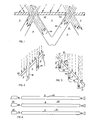
- substrate 21 is masked by photoresist 23 which is patterned to define the penetration regions for intercepting slots 25 and 26. Since substrate 21 is shown doped NPN type, the intermediate region 27 which will eventually comprise a plurality of transistors, is also of the NPN type, having been carved from the substrate by the slots 25 and 26. To prevent intermediate region 27, better defined as a semi-array of transistor regions, from falling into substrate 21, it should be noted that the slots 25 and 26 are interrupted to leave shoulders at spaced apart intervals therealong, best seen at 31, 32 and 33 in Fig. 4.
- the masking layer 23 is a material with a low sputtering rate such as one of the heavier metals.
- Figures 2 and 3 illustrate the ease of forming intercepting slots such as 25 and 26 simply by orienting the substrate at angles, e.g. 60° to the horizontal, such that the ion flux 37 may remain in its vertical pattern to form first slots 26 and thereafter slots 25 simply by rotating the substrate 21 90°.
- triangular array 27 is shown as being substantially equalateral, it need not be and the angles may be varied to configure the active regions as desired for specific purposes. It will also be noticed from Figs. 2 and 3 that slots 25 and 26 terminate where they intercept because extending them deeper into the substrate would serve no purpose.
- the slots 25 and 26 may be intermittent such that supporting ribs or webs 31, 32 and 3T, 32' serve to support each semi-array 27. ,These webs or supports may be at spaced apart locations along the slots 25 and 26 or merely comprise only supports at the edges of the chips because they serve but a temporary purpose as the slots will be filled with substratetoxide to provide the permanent support for each transistor region.
- the oxidation step is shown in Fig. 5 wherein silicon oxide 25' and 26' fill the respective slots 25 and 26. Also, an upper layer of silicon oxide 28 covers the upper surface and is contiguous with the silicon oxide 25' and 26' such that semi-array 27 is totally isolated from the substrate 21 by the silicon oxide and the periphery of the semi-arrays 27 are substantially covered by the oxide.
- orthogonal slots 41 divide the semi-arrays 27 into the individual transistor regions 27' and provide ingress for the doping to follow.
- each orthogonal slot 41 includes sidewalls 41' through which individual transistor region 27' will be doped.
- the other sidewalls of slots 41 provide for doping adjacent transistor regions 27'.
- Slots 41 may be-ion milled using the masking technique heretofore employed, Consequently photoresist 43 of a heavier metal is patterned as shown in Fig. 7 to provide for ion milling slots 41 via the openings 45 in the heavy photoresist 43 and silicon layer. The ion flux is illustrated by the lines 46.
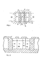
- an individual transistor region 27' is shown comprising the N+ doped region 51, P doped region 52 and N+ doped region 53.
- the P region 52 is the base region and comprises a portion of the original substrate 21.
- both N+ regions 51 and 53 are provided by doping region 27' via the sidewalls 41' of orthogonal slots 41 (Fig 6) with phosphorous deposition, diffusion or implantation plus drive-in to create the emitter region 51 and the collector region 53.
- the structure of Fig. 8 is oxidized to fill in slots 41 with silicon oxide 54 and covering layer 55.
- FIG. 8 A slight variation of the structure of Fig. 8 is indicated by the dotted line 60 wherein the P region 52 may comprise a P+ region 61 and a P region 60 simply by providing a boron doping via the left hand sidewall 4T prior to the phosphorous doping and then driving in the P+ region 61 such that the base will now comprise a graded P+P region 61, 62.
- Fig. 9 The next step in the process is illustrated in Fig. 9 wherein the silicon oxide layer 55 has been patterned and metallization applied to comprise the emitter electrode 71, base electrode 72 and collector electrode 73. However, prior to applying the metallization, a light boron deposit has been made in the base region 52 to provide the P+ base spanning region 75.
- the purpose of the boron deposition 75 prior to the metallization is twofold i.e. first to reduce the base region contact resistance and second to produce a potential barrier Pf that will deflect the electrons in transit across the base region 52 away from the base contact.
- FIG. 10 another innovation is shown in the form of the P+ skin 77 about the periphery of the individual transistor active region 27'.
- the P+ skin is formed by a light boron deposition for the purpose of keeping the electrons away from the base periphery and urging them toward the central part of the base region 52. This reduces surface recombination and thus, increases gain, especially for operation at currents in the nanoampere range.
- Figure 11 shows a completed transistor in accordance with the general principles of the invention wherein the active region 27' is shown totally surrounded by the silicon oxide 101 and the electrodes 71, 72 and 73 for the emitter region 51, base region 52 and collector 53 are seen in top plan view. Also, the P+ base spanning region 75 is seen in plan across base region 52.
- the transistor is reduced to just its electronically active area.
- the drift field P+,P in the base region 52 was produced such as is found in conventional double diffused devices.
- an NPN device can be built utilizing an N-type substrate in the manner of having built the PNP device starting from a P substrate as described. This is shown in Fig. 12 wherein all doping is accomplished through the sidewalls 41" of the orthogonal slots, as previously explained.
- the P+ region 106 is formed via angled implanting through the left hand sidewall 41" of boron material, followed by heating to drive in region 106 to its position shown in Fig. 12 adjacent an original portion 107 of the N substrate.
- phosphorous doping is carried out through both sidewalls 41'' to form the emitter region 111 doped N+ and the remaining portion of the collector region doped N+ and shown at 112 which taken together within region 107 comprises the collector.
- Patterning of the silicon oxide on the top of this device has been shown and it is only necessary to lay down the metallization pattern for electrical connection to the various transistor regions.
- a lateral, dielectrically isolated NPN transistor with a drift field in the base and an NN+ collector region has been formed with all the characteristics heretofore attributed to these submicron devices.
- the invention may be summarized as follows:
Landscapes
- Bipolar Transistors (AREA)
- Element Separation (AREA)
Applications Claiming Priority (2)
| Application Number | Priority Date | Filing Date | Title |
|---|---|---|---|
| US23975081A | 1981-03-02 | 1981-03-02 | |
| US239750 | 1981-03-02 |
Publications (1)
| Publication Number | Publication Date |
|---|---|
| EP0059266A2 true EP0059266A2 (de) | 1982-09-08 |
Family
ID=22903564
Family Applications (1)
| Application Number | Title | Priority Date | Filing Date |
|---|---|---|---|
| EP81110534A Withdrawn EP0059266A2 (de) | 1981-03-02 | 1981-12-17 | Lateraler Transistor, isoliert vom Substrat durch gekreuzte, mit einem Oxid des Substrats gefüllte Rillen, zum Minimalisieren der Substratinterferenzen und Verfahren zu dessen Herstellung |
Country Status (2)
| Country | Link |
|---|---|
| EP (1) | EP0059266A2 (de) |
| JP (1) | JPS57157570A (de) |
Cited By (1)
| Publication number | Priority date | Publication date | Assignee | Title |
|---|---|---|---|---|
| GB2198285A (en) * | 1986-12-01 | 1988-06-08 | Mitsubishi Electric Corp | Bipolar transistor |
Families Citing this family (2)
| Publication number | Priority date | Publication date | Assignee | Title |
|---|---|---|---|---|
| US4510676A (en) * | 1983-12-06 | 1985-04-16 | International Business Machines, Corporation | Method of fabricating a lateral PNP transistor |
| JPH0665218B2 (ja) * | 1984-03-13 | 1994-08-22 | 三菱電機株式会社 | 薄膜トランジスタの製造方法 |
-
1981
- 1981-12-17 EP EP81110534A patent/EP0059266A2/de not_active Withdrawn
-
1982
- 1982-02-25 JP JP57030457A patent/JPS57157570A/ja active Pending
Cited By (3)
| Publication number | Priority date | Publication date | Assignee | Title |
|---|---|---|---|---|
| GB2198285A (en) * | 1986-12-01 | 1988-06-08 | Mitsubishi Electric Corp | Bipolar transistor |
| GB2198285B (en) * | 1986-12-01 | 1990-08-01 | Mitsubishi Electric Corp | Bipolar transistor and method of manufacturing the same |
| US4990991A (en) * | 1986-12-01 | 1991-02-05 | Mitsubishi Denki Kabushiki Kaisha | Bipolar transistor and method of manufacturing the same |
Also Published As
| Publication number | Publication date |
|---|---|
| JPS57157570A (en) | 1982-09-29 |
Similar Documents
| Publication | Publication Date | Title |
|---|---|---|
| US4458158A (en) | IC Including small signal and power devices | |
| US4466178A (en) | Method of making extremely small area PNP lateral transistor by angled implant of deep trenches followed by refilling the same with dielectrics | |
| US4419150A (en) | Method of forming lateral bipolar transistors | |
| US20040164304A1 (en) | Insulated gate planar integrated power device with co-integrated schottky diode and process | |
| JPH0336311B2 (de) | ||
| US4415371A (en) | Method of making sub-micron dimensioned NPN lateral transistor | |
| US4510676A (en) | Method of fabricating a lateral PNP transistor | |
| EP0068071A1 (de) | Durchbruchdioden für Spannungsregelung und Verfahren zur Herstellung | |
| US4966858A (en) | Method of fabricating a lateral semiconductor structure including field plates for self-alignment | |
| US4584762A (en) | Lateral transistor separated from substrate by intersecting slots filled with substrate oxide for minimal interference therefrom and method for producing same | |
| US4435899A (en) | Method of producing lateral transistor separated from substrate by intersecting slots filled with substrate oxide | |
| US5726069A (en) | Use of oblique implantation in forming emitter of bipolar transistor | |
| US5198376A (en) | Method of forming high performance lateral PNP transistor with buried base contact | |
| US4485551A (en) | NPN Type lateral transistor separated from substrate by O.D.E. for minimal interference therefrom and method for producing same | |
| US6573550B2 (en) | Semiconductor with high-voltage components and low-voltage components on a shared die | |
| JPH0413863B2 (de) | ||
| US5031014A (en) | Lateral transistor separated from substrate by intersecting slots filled with substrate oxide for minimal interference therefrom | |
| US4497685A (en) | Small area high value resistor with greatly reduced parasitic capacitance | |
| EP0069191A1 (de) | Komplementäre NPN- und PNP- Lateraltransistoren, die zur minimalen Beeinflussung durch mit Substratoxyd gefüllte, sich kreuzende Rillen vom Substrat getrennt sind, und Verfahren zu ihrer Herstellung | |
| JPH0249025B2 (de) | ||
| US5273913A (en) | High performance lateral PNP transistor with buried base contact | |
| US4097888A (en) | High density collector-up structure | |
| EP0068073A2 (de) | Lateraler PNP Transistor mit minimaler Beeinflussung der Arbeitsweise durch das Substrat und Verfahren zu seiner Herstellung | |
| US6215167B1 (en) | Power semiconductor device employing field plate and manufacturing method thereof | |
| US3894891A (en) | Method for making a space charge limited transistor having recessed dielectric isolation |
Legal Events
| Date | Code | Title | Description |
|---|---|---|---|
| PUAI | Public reference made under article 153(3) epc to a published international application that has entered the european phase |
Free format text: ORIGINAL CODE: 0009012 |
|
| AK | Designated contracting states |
Designated state(s): DE FR GB |
|
| 17P | Request for examination filed |
Effective date: 19830308 |
|
| STAA | Information on the status of an ep patent application or granted ep patent |
Free format text: STATUS: THE APPLICATION IS DEEMED TO BE WITHDRAWN |
|
| 18D | Application deemed to be withdrawn |
Effective date: 19840703 |
|
| RIN1 | Information on inventor provided before grant (corrected) |
Inventor name: SOCLOF, SIDNEY ISAAC |