EP0069191A1 - Komplementäre NPN- und PNP- Lateraltransistoren, die zur minimalen Beeinflussung durch mit Substratoxyd gefüllte, sich kreuzende Rillen vom Substrat getrennt sind, und Verfahren zu ihrer Herstellung - Google Patents
Komplementäre NPN- und PNP- Lateraltransistoren, die zur minimalen Beeinflussung durch mit Substratoxyd gefüllte, sich kreuzende Rillen vom Substrat getrennt sind, und Verfahren zu ihrer Herstellung Download PDFInfo
- Publication number
- EP0069191A1 EP0069191A1 EP82101439A EP82101439A EP0069191A1 EP 0069191 A1 EP0069191 A1 EP 0069191A1 EP 82101439 A EP82101439 A EP 82101439A EP 82101439 A EP82101439 A EP 82101439A EP 0069191 A1 EP0069191 A1 EP 0069191A1
- Authority
- EP
- European Patent Office
- Prior art keywords
- regions
- substrate
- slots
- arrays
- sidewalls
- Prior art date
- Legal status (The legal status is an assumption and is not a legal conclusion. Google has not performed a legal analysis and makes no representation as to the accuracy of the status listed.)
- Withdrawn
Links
Images


Classifications
-
- H—ELECTRICITY
- H10—SEMICONDUCTOR DEVICES; ELECTRIC SOLID-STATE DEVICES NOT OTHERWISE PROVIDED FOR
- H10D—INORGANIC ELECTRIC SEMICONDUCTOR DEVICES
- H10D10/00—Bipolar junction transistors [BJT]
- H10D10/60—Lateral BJTs
-
- H—ELECTRICITY
- H10—SEMICONDUCTOR DEVICES; ELECTRIC SOLID-STATE DEVICES NOT OTHERWISE PROVIDED FOR
- H10B—ELECTRONIC MEMORY DEVICES
- H10B20/00—Read-only memory [ROM] devices
- H10B20/10—ROM devices comprising bipolar components
-
- H—ELECTRICITY
- H10—SEMICONDUCTOR DEVICES; ELECTRIC SOLID-STATE DEVICES NOT OTHERWISE PROVIDED FOR
- H10D—INORGANIC ELECTRIC SEMICONDUCTOR DEVICES
- H10D84/00—Integrated devices formed in or on semiconductor substrates that comprise only semiconducting layers, e.g. on Si wafers or on GaAs-on-Si wafers
- H10D84/01—Manufacture or treatment
- H10D84/0112—Integrating together multiple components covered by H10D8/00, H10D10/00 or H10D18/00, e.g. integrating multiple BJTs
-
- H—ELECTRICITY
- H10—SEMICONDUCTOR DEVICES; ELECTRIC SOLID-STATE DEVICES NOT OTHERWISE PROVIDED FOR
- H10D—INORGANIC ELECTRIC SEMICONDUCTOR DEVICES
- H10D84/00—Integrated devices formed in or on semiconductor substrates that comprise only semiconducting layers, e.g. on Si wafers or on GaAs-on-Si wafers
- H10D84/01—Manufacture or treatment
- H10D84/02—Manufacture or treatment characterised by using material-based technologies
- H10D84/03—Manufacture or treatment characterised by using material-based technologies using Group IV technology, e.g. silicon technology or silicon-carbide [SiC] technology
- H10D84/038—Manufacture or treatment characterised by using material-based technologies using Group IV technology, e.g. silicon technology or silicon-carbide [SiC] technology using silicon technology, e.g. SiGe
-
- H—ELECTRICITY
- H10—SEMICONDUCTOR DEVICES; ELECTRIC SOLID-STATE DEVICES NOT OTHERWISE PROVIDED FOR
- H10P—GENERIC PROCESSES OR APPARATUS FOR THE MANUFACTURE OR TREATMENT OF DEVICES COVERED BY CLASS H10
- H10P30/00—Ion implantation into wafers, substrates or parts of devices
- H10P30/20—Ion implantation into wafers, substrates or parts of devices into semiconductor materials, e.g. for doping
- H10P30/22—Ion implantation into wafers, substrates or parts of devices into semiconductor materials, e.g. for doping using masks
- H10P30/221—Ion implantation into wafers, substrates or parts of devices into semiconductor materials, e.g. for doping using masks characterised by the angle between the ion beam and the mask
-
- H—ELECTRICITY
- H10—SEMICONDUCTOR DEVICES; ELECTRIC SOLID-STATE DEVICES NOT OTHERWISE PROVIDED FOR
- H10P—GENERIC PROCESSES OR APPARATUS FOR THE MANUFACTURE OR TREATMENT OF DEVICES COVERED BY CLASS H10
- H10P30/00—Ion implantation into wafers, substrates or parts of devices
- H10P30/20—Ion implantation into wafers, substrates or parts of devices into semiconductor materials, e.g. for doping
- H10P30/222—Ion implantation into wafers, substrates or parts of devices into semiconductor materials, e.g. for doping characterised by the angle between the ion beam and the crystal planes or the main crystal surface
-
- H—ELECTRICITY
- H10—SEMICONDUCTOR DEVICES; ELECTRIC SOLID-STATE DEVICES NOT OTHERWISE PROVIDED FOR
- H10W—GENERIC PACKAGES, INTERCONNECTIONS, CONNECTORS OR OTHER CONSTRUCTIONAL DETAILS OF DEVICES COVERED BY CLASS H10
- H10W10/00—Isolation regions in semiconductor bodies between components of integrated devices
- H10W10/01—Manufacture or treatment
- H10W10/011—Manufacture or treatment of isolation regions comprising dielectric materials
- H10W10/014—Manufacture or treatment of isolation regions comprising dielectric materials using trench refilling with dielectric materials, e.g. shallow trench isolations
- H10W10/0148—Manufacture or treatment of isolation regions comprising dielectric materials using trench refilling with dielectric materials, e.g. shallow trench isolations comprising introducing impurities in side walls or bottom walls of trenches, e.g. for forming channel stoppers
-
- H—ELECTRICITY
- H10—SEMICONDUCTOR DEVICES; ELECTRIC SOLID-STATE DEVICES NOT OTHERWISE PROVIDED FOR
- H10W—GENERIC PACKAGES, INTERCONNECTIONS, CONNECTORS OR OTHER CONSTRUCTIONAL DETAILS OF DEVICES COVERED BY CLASS H10
- H10W10/00—Isolation regions in semiconductor bodies between components of integrated devices
- H10W10/10—Isolation regions comprising dielectric materials
- H10W10/17—Isolation regions comprising dielectric materials formed using trench refilling with dielectric materials, e.g. shallow trench isolations
Definitions
- This invention is a novel structure and method for forming sub-micron type lateral dielectrically isolated complementary transistors utilizing VLSI chip processing steps to compatibly fabricate hundreds of such devices, simultaneously on a common functional chip.
- the invention comprises novel lateral complementary transistors formed on a selectively doped substrate by intersecting slots and orthogonal slots for respectively defining each active region undercut by selective intersecting slots and filled with substrate oxide to isolate the effective regions from the substrate.
- selective doping is introduced by angle implantation from opposed orthogonal surfaces of each individual active region to complete the NPN formations or the complementary PNP formations.
- the intersecting slots and the orthogonal slots of the complementary devices are respectively orthogonally related. Electrical connections are made in conventional fashion to become emitter, base and collector regions.
- FIGURE 8A illustrates angled doping
- the effects of the substrate are minimized relative to the operation of the devices.
- Each active region is completely separated from the substrate by substrate oxidation and the parasitic capacitances and resistances are almost completely reduced to a minimum value attainable because the transistors are reduced to just their electronically active regions.
- the electrically active region is only a very small fraction of the total transistor area or volume.
- the dielectric isolation between transistors offered by the substrate oxidation has advantages with respect to high frequency performance, high voltage integrated circuits, radiation resistance, and circuit flexibility, i.e., the process provides NPN and PNP devices on the same integrated circuit chip.
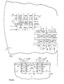
- the chip or die is partly shown at 1 carrying an NPN formation of transistors structures 2 and a separate PNP formation of transistor structures 3.
- a pair of intersecting slots 4 and 5 form triangular shaped active regions 6 and 7 separated by orthogonal slots 8 and 9.
- the arrows 10 and 11 illustrate the angle doping paths (when -tilted upwardly) for N or N+ doping of the underlying substrate.
- slots 8 and 9 are also filled with oxide and electrical connections are established to the electrode regions of the isolated -active transistor regions.
- the intersecting slots 12 and 13 of the P region are illustrated orthogonal to intersecting slots 4 and 5 of the N region 2, and the directions of angled doping, shown by arrows 14 and 15, is at right angles to arrows 10 and 11 of region 2. Since ion milling and ion doping are preferably employed, many regions, such as 2 and 3, may be selectively distributed across the chip 1, and accurately indexed by present day conventional techniques. This offers versatility of association of the complementary transistors. Use of the ullistrated orthogonal relationship of slots 8 and 9 to slots 101 and 102 serves to prevent contaminating of doping (i.e.) N type doping is only Injected at right angles to P type doping.
- substrate 21 is masked by photoresist 23 which is patterned to define the penetration regions for intersecting slots 25 and 26. Since substrate 21 is shown doped N-or P type, the intermediate region 27 will eventually comprise a plurality of transistors of either the NPN or PNP type, having been carved from the substrate by the slots 25 and 26. To prevent intermediate region 27, better defined as a semi-array of transistor regions, from falling into substrate 21, it should be noted that the slots 25 and 26 are interrupted to leave shoulders at spaced apart intervals therealong, best seen at 31, 32 and 33 in Fig. 5.
- the masking layer 23 is a material with a low sputtering rate, such as one of the heavier metals.
- FIGS 3 and 4 illustrate the ease of forming Intersecting slots, such as 25 and 26,simply by orienting the substrate at angles, e.g., 60° to the horizontal, such that the ion flux 37 may remain in its vertical pattern to form, first slots 26, and thereafter slots 25 simply by rotating the substrate 21 through 90°.
- the flux may be accurately directed to any region 2 or 3.
- triangular array 27 is shown as being substantially equilateral, it need not be and the angles may be varied to configure the active regions as desired for specific purposes, It will also be noticed from Figs. 3 and 4 that slots 25 and 26 terminate where they intersect because extending them deeper into the substrate would serve no purpose.
- the slots 25 and 26 may be intermittent such that supporting ribs or webs 31, 32 and 31', 32' serve to support each semi-array 27.
- These webs or supports may be at spaced apart locations along the slots 25 and 26 or merely comprise only supports at the edges of the chips because they serve but a temporary purpose as the slots will be filled with substrate oxide to provide the permanent support for each transistor region.
- the first oxidation step is shown in Fig. 6 wherein silicon oxide 25' and 26' fills the respective slots 25 and 26. Also, an upper layer of silicon oxide 28 (Fig. 6) covers the upper surface and is continguous with the silicon oxide 25' and 26' such that semi-array 27 is totally isolated from the substrate 21 by the silicon oxide, and the periphery of the semi-arrays 27 are substantially covered by the oxide.
- orthogonal slots 41 divide the semi-arrays 27 into the individual transistor regions 27' and provide ingress for the doping to follow.
- each orthogonal slots 41 includes sidewalls 41' through which individual transistor regions 27' will be doped.
- the other sidewalls 41" of slots 41 provide for doping adjacent transistor regions 27'.
- Slots 41 may be ion milled using the masking technique heretofore employed. Consequently, photoresist 43 (fig. 8) of a heavier metal is patterned as shown in Fig. 8 to provide for ion milling slots 41 via the openings 45 in the heavy photoresist 43 and silicon oxide layer 42. The ion flux is illustrated by the lines 46.
- Fig. 8A it may be seen that the N+ regions 31 and 33 are implanted by ion implanting at an angle as illustrated by the ion beams 32 and 34. It is important to note that the angle of the ion beams relative to the slot directions is such that the N+ implanting does not extend to the full depth of the slots 23 and 25. Actually the corners of the silicon oxide layer 42 form a shadowing effect and cooperate with the orientation of the beams 32 and 34 in fixing the N+ doped regions within the P active region 27. Phosphor or other donors may be employed in this step. Dotted lines 31' and 33' show that the doping has been driven in and the N+ regions 31 and 33 considerably enlarged. This may be accomplished through the applica-, tion of heat over a controlled period of time and temperature.
- an individual transistor region 27' is shown comprising N or N+ doped region 51, P or P+ doped region 52 and N or N+ doped region 53.
- the P region 52 is the base region and comprises a portion of the original substrate 21, e.g., doped P.at formation 2 in Fig. 1.
- both N+ regions 51 and 53 are provided by doping region 27' via the sidewalls 41' and 41" of orthogonal slots 41 (Fig. 7) with phosphorous deposition, diffusion or implantation plus drive-in to create the emitter region 51 and the collector region 53.
- the structure of Fig. 9 is oxidized to fill in slots 41 with silicon oxide 54 and provide covering layer 51.
- Fig. 10 The next step in the process is illustrated in Fig. 10 wherein the silicon oxide layer 51 has been patterned to leave oxide islands 55 and metallization applied to comprise the emitter electrode 71, base electrode 72 and collector electrode 73.
- a light boron deposit may be made in the base region 52 to provide the P+ base spanning region 75, if desired.
- the purpose of the boron deposition 75 prior to the metallization is two fold, i.e., first to reduce the base region contact resistance and second to produce a potential barrier P+ that will deflect the electrons in transit across the base region 52 away from the base contact.
- a PNP device can be built utilizing a P-type substrate in the manner of having built the NPN device starting from a P substrate as described in region 3 Fig. 1. This is shown in Fig. 11 wherein emitter region 85 is conventionally P doped, but by angled ion flux via the slots 101, 102 (Fig. 1) just as in the process for the NPN transistors. Collector region 86 is similarly formed, and base region 87 is part of the original N doped substrate 3 (Fig. 1).
- Interconnections of the complementary transistors may be established using conventional diffused lines, poly lines or metal patterning.
- N and P formations need not be at right angles but this arrangement insures that ion doping is carried out most efficiently and there are no components of doping intended for NPN transistors which dope the complementary PNP transistors. This orientation facilitates higher speed and more efficient processing.
Landscapes
- Bipolar Transistors (AREA)
- Bipolar Integrated Circuits (AREA)
Applications Claiming Priority (2)
| Application Number | Priority Date | Filing Date | Title |
|---|---|---|---|
| US27746581A | 1981-06-25 | 1981-06-25 | |
| US277465 | 1981-06-25 |
Publications (1)
| Publication Number | Publication Date |
|---|---|
| EP0069191A1 true EP0069191A1 (de) | 1983-01-12 |
Family
ID=23060993
Family Applications (1)
| Application Number | Title | Priority Date | Filing Date |
|---|---|---|---|
| EP82101439A Withdrawn EP0069191A1 (de) | 1981-06-25 | 1982-02-25 | Komplementäre NPN- und PNP- Lateraltransistoren, die zur minimalen Beeinflussung durch mit Substratoxyd gefüllte, sich kreuzende Rillen vom Substrat getrennt sind, und Verfahren zu ihrer Herstellung |
Country Status (2)
| Country | Link |
|---|---|
| EP (1) | EP0069191A1 (de) |
| JP (1) | JPS583279A (de) |
Cited By (3)
| Publication number | Priority date | Publication date | Assignee | Title |
|---|---|---|---|---|
| EP0512607A3 (en) * | 1991-05-03 | 1993-09-08 | N.V. Philips' Gloeilampenfabrieken | Method of manufacturing a semiconductor device using ion implantation |
| US5405454A (en) * | 1992-03-19 | 1995-04-11 | Matsushita Electric Industrial Co., Ltd. | Electrically insulated silicon structure and producing method therefor |
| US5855493A (en) * | 1996-03-11 | 1999-01-05 | The Whitaker Corporation | Electrical connector strain relief with shield ground for multiple cables |
Families Citing this family (1)
| Publication number | Priority date | Publication date | Assignee | Title |
|---|---|---|---|---|
| EP0068070A1 (de) * | 1981-07-01 | 1983-01-05 | Rockwell International Corporation | Komplementare NPN- und PNP-Lateraltransistoren, die zur minimalen Beeinflussung durch mit Substratoxyd gefüllte Rillen vom Substrat getrennt sind, und Verfahren zu ihrer Herstellung |
Citations (3)
| Publication number | Priority date | Publication date | Assignee | Title |
|---|---|---|---|---|
| US4104090A (en) * | 1977-02-24 | 1978-08-01 | International Business Machines Corporation | Total dielectric isolation utilizing a combination of reactive ion etching, anodic etching, and thermal oxidation |
| EP0004298A1 (de) * | 1978-03-02 | 1979-10-03 | Western Electric Company, Incorporated | Verfahren zur Herstellung von Isolierung und Kontaktierung vergrabener Schichten von Halbleiterstrukturen |
| US4214315A (en) * | 1979-03-16 | 1980-07-22 | International Business Machines Corporation | Method for fabricating vertical NPN and PNP structures and the resulting product |
-
1982
- 1982-02-25 EP EP82101439A patent/EP0069191A1/de not_active Withdrawn
- 1982-06-17 JP JP57106068A patent/JPS583279A/ja active Pending
Patent Citations (3)
| Publication number | Priority date | Publication date | Assignee | Title |
|---|---|---|---|---|
| US4104090A (en) * | 1977-02-24 | 1978-08-01 | International Business Machines Corporation | Total dielectric isolation utilizing a combination of reactive ion etching, anodic etching, and thermal oxidation |
| EP0004298A1 (de) * | 1978-03-02 | 1979-10-03 | Western Electric Company, Incorporated | Verfahren zur Herstellung von Isolierung und Kontaktierung vergrabener Schichten von Halbleiterstrukturen |
| US4214315A (en) * | 1979-03-16 | 1980-07-22 | International Business Machines Corporation | Method for fabricating vertical NPN and PNP structures and the resulting product |
Cited By (4)
| Publication number | Priority date | Publication date | Assignee | Title |
|---|---|---|---|---|
| EP0512607A3 (en) * | 1991-05-03 | 1993-09-08 | N.V. Philips' Gloeilampenfabrieken | Method of manufacturing a semiconductor device using ion implantation |
| US5405454A (en) * | 1992-03-19 | 1995-04-11 | Matsushita Electric Industrial Co., Ltd. | Electrically insulated silicon structure and producing method therefor |
| US5543351A (en) * | 1992-03-19 | 1996-08-06 | Matsushita Electric Industrial Co., Ltd. | Method of producing electrically insulated silicon structure |
| US5855493A (en) * | 1996-03-11 | 1999-01-05 | The Whitaker Corporation | Electrical connector strain relief with shield ground for multiple cables |
Also Published As
| Publication number | Publication date |
|---|---|
| JPS583279A (ja) | 1983-01-10 |
Similar Documents
| Publication | Publication Date | Title |
|---|---|---|
| US4437226A (en) | Process for producing NPN type lateral transistor with minimal substrate operation interference | |
| US4038680A (en) | Semiconductor integrated circuit device | |
| US4466178A (en) | Method of making extremely small area PNP lateral transistor by angled implant of deep trenches followed by refilling the same with dielectrics | |
| US4458158A (en) | IC Including small signal and power devices | |
| US4419150A (en) | Method of forming lateral bipolar transistors | |
| US4115797A (en) | Integrated injection logic with heavily doped injector base self-aligned with injector emitter and collector | |
| JPH0336311B2 (de) | ||
| US4522682A (en) | Method for producing PNP type lateral transistor separated from substrate by O.D.E. for minimal interference therefrom | |
| US4415371A (en) | Method of making sub-micron dimensioned NPN lateral transistor | |
| EP0068071A1 (de) | Durchbruchdioden für Spannungsregelung und Verfahren zur Herstellung | |
| KR0139005B1 (ko) | 상보형 바이폴라와 상보형 mos를 병합한 수단 및 그 제조방법 | |
| US4988639A (en) | Method of manufacturing semiconductor devices using trench isolation method that forms highly flat buried insulation film | |
| US4584762A (en) | Lateral transistor separated from substrate by intersecting slots filled with substrate oxide for minimal interference therefrom and method for producing same | |
| KR890003474B1 (ko) | Soi기판상에 형성된 래터럴 바이폴라 트랜지스터 | |
| US4485551A (en) | NPN Type lateral transistor separated from substrate by O.D.E. for minimal interference therefrom and method for producing same | |
| US4435899A (en) | Method of producing lateral transistor separated from substrate by intersecting slots filled with substrate oxide | |
| EP0069191A1 (de) | Komplementäre NPN- und PNP- Lateraltransistoren, die zur minimalen Beeinflussung durch mit Substratoxyd gefüllte, sich kreuzende Rillen vom Substrat getrennt sind, und Verfahren zu ihrer Herstellung | |
| US5198376A (en) | Method of forming high performance lateral PNP transistor with buried base contact | |
| US4704786A (en) | Method of forming a lateral bipolar transistor in a groove | |
| JPH0413863B2 (de) | ||
| US4506283A (en) | Small area high value resistor with greatly reduced parasitic capacitance | |
| US4497685A (en) | Small area high value resistor with greatly reduced parasitic capacitance | |
| US5031014A (en) | Lateral transistor separated from substrate by intersecting slots filled with substrate oxide for minimal interference therefrom | |
| EP0059266A2 (de) | Lateraler Transistor, isoliert vom Substrat durch gekreuzte, mit einem Oxid des Substrats gefüllte Rillen, zum Minimalisieren der Substratinterferenzen und Verfahren zu dessen Herstellung | |
| US4611387A (en) | Process for producing NPN type lateral transistors |
Legal Events
| Date | Code | Title | Description |
|---|---|---|---|
| PUAI | Public reference made under article 153(3) epc to a published international application that has entered the european phase |
Free format text: ORIGINAL CODE: 0009012 |
|
| 17P | Request for examination filed |
Effective date: 19820630 |
|
| AK | Designated contracting states |
Designated state(s): DE FR GB |
|
| STAA | Information on the status of an ep patent application or granted ep patent |
Free format text: STATUS: THE APPLICATION IS DEEMED TO BE WITHDRAWN |
|
| 18D | Application deemed to be withdrawn |
Effective date: 19840830 |
|
| RIN1 | Information on inventor provided before grant (corrected) |
Inventor name: SOCLOF, SIDNEY ISAAC |