EP0060115B1 - Circuit de mémoire statique RAM - Google Patents
Circuit de mémoire statique RAM Download PDFInfo
- Publication number
- EP0060115B1 EP0060115B1 EP82301156A EP82301156A EP0060115B1 EP 0060115 B1 EP0060115 B1 EP 0060115B1 EP 82301156 A EP82301156 A EP 82301156A EP 82301156 A EP82301156 A EP 82301156A EP 0060115 B1 EP0060115 B1 EP 0060115B1
- Authority
- EP
- European Patent Office
- Prior art keywords
- field effect
- data bus
- pair
- effect transistors
- memory circuit
- Prior art date
- Legal status (The legal status is an assumption and is not a legal conclusion. Google has not performed a legal analysis and makes no representation as to the accuracy of the status listed.)
- Expired
Links
Images

Classifications
-
- G—PHYSICS
- G11—INFORMATION STORAGE
- G11C—STATIC STORES
- G11C11/00—Digital stores characterised by the use of particular electric or magnetic storage elements; Storage elements therefor
- G11C11/21—Digital stores characterised by the use of particular electric or magnetic storage elements; Storage elements therefor using electric elements
- G11C11/34—Digital stores characterised by the use of particular electric or magnetic storage elements; Storage elements therefor using electric elements using semiconductor devices
- G11C11/40—Digital stores characterised by the use of particular electric or magnetic storage elements; Storage elements therefor using electric elements using semiconductor devices using transistors
- G11C11/41—Digital stores characterised by the use of particular electric or magnetic storage elements; Storage elements therefor using electric elements using semiconductor devices using transistors forming static cells with positive feedback, i.e. cells not needing refreshing or charge regeneration, e.g. bistable multivibrator or Schmitt trigger
- G11C11/413—Auxiliary circuits, e.g. for addressing, decoding, driving, writing, sensing, timing or power reduction
- G11C11/417—Auxiliary circuits, e.g. for addressing, decoding, driving, writing, sensing, timing or power reduction for memory cells of the field-effect type
- G11C11/419—Read-write [R-W] circuits
Definitions
- the present invention relates to a static RAM (Random Access Memory) memory circuit.
- D1 discloses an arrangement in which, in a RAM using MOS transistors, outputs of transistors connected to digit lines are fed back via a latch circuit and NAND gates to digit line load transistors.
- D2 discloses a discharging circuit for discharging a bit line of an MOS memory.
- D3 discloses a symmetrical differential amplifying circuit for an asynchronous complementary type RAM.
- D4 discloses memory and sense amplifier circuitry of a static MOS RAM.
- D5 concerns a static type MIS memory and a circuit for reducing power consumption when writing.
- a static RAM including a memory circuit comprising: a pair of bit lines, to which pull-up loads are respectively connected; a plurality of memory cells each connected to the pair of bit lines; a pair of data bus lines operatively connected to the pair of bit lines, and a sense amplifier connected to the pair of bit lines through the pair of data bus lines, characterised in that the sense amplifier comprises a linear amplifier which delivers complementary outputs and in that the memory circuit further comprises charging circuitry operatively connected to the pair of data bus lines for charging up that one of the pair of data bus lines which is of higher potential, the charging circuitry having control terminals arranged to receive respectively and directly the complementary outputs of the sense amplifier and being activated in dependence upon the said outputs.
- An embodiment of the present invention can provide a high-density static RAM capable of fast operation.
- a load of a data bus line which line may be regarded as equivalent to a bit line in terms of potential changes etc. because it is connected to the bit line through a column selecting gate, (the load being a pull-up FET for example) in other words a charging current, is changed in dependence upon a signal read out.
- Figure 1 illustrates an embodiment of the present invention.
- MC indicates memory cells
- SA is a sense amplifier.
- X o -X N are word lines
- Y O -Y N are column selecting signal lines.
- Q 1 ⁇ Q 4 are MOS FET's forming column selecting gates
- Q 5 and Q 6 are MIS FET's (hereinafter referred to as MOS FET's) which are as bit line loads.
- Q 7 and Q 8 are MOS FET's which constitute a cell driver, and are respectively provided with load elements (resistors) R 1 and R2.
- Q 9 and Q lo are MOS FET's which function as transfer gates.
- BL and BL are a bit line pair
- DB and DB are a pair of data bus lines.
- Q 11 and Q 12 are MOS FET's of charging circuits for charging the data bus lines DB and DB, respectively.
- the sense amplifier SA is a differantial amplifier comrising two inverters made up of depletion- mode load MOS FET's Q 13 and Q 14 and enhancement-mode driving MOS FET's Q 15 and Q 16 .
- the sources of MOS FET's Q 15 and Q 16 are connected in common.
- Q 17 and Q 18 are MOS FET's which are connected in parallel with one another to the common-connected sources of Q, 5 and Q 16 .
- Outputs DF and DF (of the inverters) are fed back to the MOS FET's Q 17 and Q 18 , to correct a reference voltage V ref (at their common connection point with the sources of Q 15 and Q 16 ) to provide an appropriate value at all times so that a linear operation is effected.
- An input of the sense amplifier SA on the side of the MOS FET Q 15 is the potential of the data bus line DB, whilst an input of the sense amplifier SA on the side of the MOS FET Q 16 is the potential of the data bus line DB.
- An amplified output DF of the same polarity as the potential of the data bus line DB, is obtained from the drain side of the MOS FET Q 15 , and is fed back to the gate of the MOS FET Q 11 .
- an amplified output DF of the same polarity as the potential of the data bus line DB, is obtained from the drain side of the MOS FET Q 16 , and is fed back to the gate of the MOS FET Q 12 .
- V cc signifies a power source voltage
- a downwardly pointing arrow signifies ground.
- the outputs DF and DF are respectively fed back to the gates of the MOS FET's Q 17 and Q 18 .
- the reference voltage V ref can become a virtual ground or a constant voltage with respect to the inputs DB and DB.
- the reference voltage V ref is in phase with supply voltage: that is to say, the reference voltage V, ef rises with an increase in supply voltage (V cc ) and falls with a decrease in power source voltage.
- this differential amplifier generates amplified outputs DF and DF which follow up the fluctuations. That is, the amplifier operates as an analog linear amplifier in which, when the input DB changes from “L” (low level) to "H” (high level) and the input DB changes from “H” to “L”, the output DF rapidly shifts from “H” to “L” and the output DF rapidly shifts from “L” to “H”.
- the outputs DF and DF are respectively fed back to the gates of the MOS FETs Q 11 and Q 12 in the same polarity (with unchanged polarities).
- the potential changes of a data bus line and a bit line which are shifting from “L” to "H", for example DB and BL, are promoted by charging using the MOS FET Q 11 (DF) and are therefore effected quickly. This is equivalent to temporarily increasing the transconductance g m of the bit line load transistor Q 5 (of bit line BL) during charging.
- the MOS FET Q 12 has its gate supplied with the amplified output DB (DF), which is changing from “H” to “L”, and turns “OFF". Therefore, the discharging characteristics of the data bus line DB and the biz line BL are those based only on the bit line load MOS FET Q 6 and are unaffected by Q 12 . Since the transconductance G M OF THE MOS FET Q 6 remains low, the pull-down of the data bus line and bit line is satisfactorily effected by the cell driver MOS FET Q e .
- Figure 1 OB is an output buffer which receives the signals DF, DF and outputs a read out signal to an output terminal OUT.
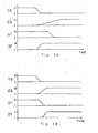
- Figures 3A and 3B are signal waveform diagrams showing the variations of data bus line signals DB, DB and output signals DF, DF in a previously proposed circuit and in an embodiment of the present invention, respectively.
- the previously proposed circuit does not comprise the charging transistors Q 11 , Q 12 of Figure 1.
- the signal DB changes from "H” to "L” rapidly, but the signal DB changes from "L” to “H” slowly.
- the reason for this is that the discharging ability of transistor Q 7 (Q 8 ) is better than the charging ability of transistor Q 6 (Q 5 ) in general.
- a charging MOS FET connected to the data bus line on the "H” side turns “ON” and performs a pull-up operation, but the charging MOS FET connected to the data bus line on the "L” side turns “OFF” and has no effect on operations.
- the "ON" MOS FET of the selected cell pulls- down the bit line and the data bus line on the "H" side (as determined by the previously selected cell-BL and DB in this case).
- MOS FET Q11 since the presence of MOS FET Q11 is to be considered, the pull-down load becomes greater than in the previously proposed circuit.
- the presence of the MOS FET Q1' causes no special problems for reasons described hereunder.
- the sense amplifier SA of a memory circuit embodying the present invention is a linear amplifier which has the widest possible range of proportional operation as described above. Therefore, as soon as the bit line and the data bus line begin to change their potential levels, the sense amplifier SA starts operating so as to promote those changes.
- each memory cell has the transconductance g m ratio between the driver MOS FET's Q 7 and Q s and the transfer gate MOS FET's Q 9 , Q 10 properly selected so that the bit line and the data bus line when close to the power source voltage as viewed from the minute cell, can be pulled down sufficiently.
- the transconductance g m of the data bus load is in effect made high during charging, and low (as usual) during discharging, so that the transconductance g m of the bit line load can be set in a ratioless form relative to the transconductance g of the cell driver. Accordingly, the signal change of the bit line is efficiently speeded up, and read-out speed is enhanced.
- read-out outputs are derived by passing the outputs DF and DF of the sense amplifier SA through the output buffer OB.
- MOS FET's Q 5 and Q 6 are used as loads. However, they can be replaced as loads by resistors. Further, whilst MOS FETs have been referred to in the description of the illustrated embodiment, embodiments using other semiconductor devices can be provided.
- a bit line load current in other words a charging current, (which is reduced when the memory has a high memory density) of a memory is changed in response to a signal to be read out, so that fast read-out is achieved even when the transconductance g m of a cell driver is low.
- An embodiment of the present invention provides a high density static RAM integrated circuit comprising a pair of bit lines to which pull-up loads are respectively connected, a plurality of memory cells which are connected across the bit lines of the pair, a pair of data buses which are connected to the pair of bit lines, and a sense amplifier which is connected to the pair of bit lines through the pair of data buses, the pair of data buses being respectively provided with charging circuits each of which has a control terminal for varying the pull-up current applied to the relevant data bus (and bit line), amplified outputs of the sense amplifier being fed back to control terminals of the charging circuits, and the data bus on a high potential side being charged by the corresponding charging circuit.
- the current to flow across a common data bus line connected to a higher (potential) side of selected bit lines is increased, thereby enabling a high speed read out operation in the high-density static RAM.
- the present invention can provide a fast-access RAM which, when reading out stored data from a memory cell, is operable to change a data bus line load in dependence upon the data to be read out, thereby to provide fast read-out.
Landscapes
- Engineering & Computer Science (AREA)
- Microelectronics & Electronic Packaging (AREA)
- Computer Hardware Design (AREA)
- Static Random-Access Memory (AREA)
Claims (7)
Applications Claiming Priority (2)
| Application Number | Priority Date | Filing Date | Title |
|---|---|---|---|
| JP56033475A JPH0831278B2 (ja) | 1981-03-09 | 1981-03-09 | メモリ回路 |
| JP33475/81 | 1981-03-09 |
Publications (3)
| Publication Number | Publication Date |
|---|---|
| EP0060115A2 EP0060115A2 (fr) | 1982-09-15 |
| EP0060115A3 EP0060115A3 (en) | 1985-04-17 |
| EP0060115B1 true EP0060115B1 (fr) | 1987-11-25 |
Family
ID=12387563
Family Applications (1)
| Application Number | Title | Priority Date | Filing Date |
|---|---|---|---|
| EP82301156A Expired EP0060115B1 (fr) | 1981-03-09 | 1982-03-08 | Circuit de mémoire statique RAM |
Country Status (5)
| Country | Link |
|---|---|
| US (1) | US4467456A (fr) |
| EP (1) | EP0060115B1 (fr) |
| JP (1) | JPH0831278B2 (fr) |
| DE (1) | DE3277749D1 (fr) |
| IE (1) | IE53339B1 (fr) |
Families Citing this family (10)
| Publication number | Priority date | Publication date | Assignee | Title |
|---|---|---|---|---|
| US4740921A (en) * | 1985-10-04 | 1988-04-26 | Motorola, Inc. | Precharge of a dram data line to an intermediate voltage |
| US4670675A (en) * | 1986-02-07 | 1987-06-02 | Advanced Micro Devices, Inc. | High gain sense amplifier for small current differential |
| US4813023A (en) * | 1986-10-21 | 1989-03-14 | Brooktree Corporation | System employing negative feedback for decreasing the response time of a cell |
| US4769564A (en) * | 1987-05-15 | 1988-09-06 | Analog Devices, Inc. | Sense amplifier |
| JP2723909B2 (ja) * | 1987-06-19 | 1998-03-09 | 株式会社日立製作所 | 半導体メモリ |
| US5293515A (en) * | 1989-09-12 | 1994-03-08 | Kabushiki Kaisha Toshiba | Amplifier circuit having two inverters |
| JPH03100996A (ja) * | 1989-09-12 | 1991-04-25 | Toshiba Micro Electron Kk | 増幅回路 |
| US5386150A (en) * | 1991-11-20 | 1995-01-31 | Fujitsu Limited | Tracking pulse generator and RAM with tracking precharge pulse generator |
| US5781469A (en) * | 1997-01-24 | 1998-07-14 | Atmel Corporation | Bitline load and precharge structure for an SRAM memory |
| US8437204B2 (en) * | 2009-06-12 | 2013-05-07 | Taiwan Semiconductor Manufacturing Company, Ltd. | Memory array with corresponding row and column control signals |
Family Cites Families (5)
| Publication number | Priority date | Publication date | Assignee | Title |
|---|---|---|---|---|
| US3765002A (en) * | 1971-04-20 | 1973-10-09 | Siemens Ag | Accelerated bit-line discharge of a mosfet memory |
| JPS54136240A (en) * | 1978-04-14 | 1979-10-23 | Nec Corp | Semiconductor integrated circuit |
| JPS5824874B2 (ja) * | 1979-02-07 | 1983-05-24 | 富士通株式会社 | センス回路 |
| JPS5833634B2 (ja) * | 1979-02-28 | 1983-07-21 | 富士通株式会社 | メモリセルアレイの駆動方式 |
| JPS6027113B2 (ja) * | 1980-02-13 | 1985-06-27 | 日本電気株式会社 | プリチャ−ジ装置 |
-
1981
- 1981-03-09 JP JP56033475A patent/JPH0831278B2/ja not_active Expired - Lifetime
-
1982
- 1982-03-01 US US06/353,332 patent/US4467456A/en not_active Expired - Lifetime
- 1982-03-08 DE DE8282301156T patent/DE3277749D1/de not_active Expired
- 1982-03-08 EP EP82301156A patent/EP0060115B1/fr not_active Expired
- 1982-03-09 IE IE529/82A patent/IE53339B1/en not_active IP Right Cessation
Non-Patent Citations (1)
| Title |
|---|
| IEEE Journal of Solid State Circuits, vol. SC-15, 1980, oct., no. 5, pages 854-861 * |
Also Published As
| Publication number | Publication date |
|---|---|
| JPH0831278B2 (ja) | 1996-03-27 |
| JPS57150185A (en) | 1982-09-16 |
| US4467456A (en) | 1984-08-21 |
| IE53339B1 (en) | 1988-10-26 |
| DE3277749D1 (en) | 1988-01-07 |
| EP0060115A3 (en) | 1985-04-17 |
| IE820529L (en) | 1982-09-09 |
| EP0060115A2 (fr) | 1982-09-15 |
Similar Documents
| Publication | Publication Date | Title |
|---|---|---|
| US5239502A (en) | Bit storage cell | |
| EP0045133B1 (fr) | Circuits d'attaque du type "bootstrap" pour une mémoire MOS | |
| US5289415A (en) | Sense amplifier and latching circuit for an SRAM | |
| US4441169A (en) | Static random access memory having a read out control circuit connected to a memory cell | |
| US4396845A (en) | Address buffer circuit | |
| EP0060115B1 (fr) | Circuit de mémoire statique RAM | |
| US5517142A (en) | Output buffer with a reduced transient bouncing phenomenon | |
| JPH0355913B2 (fr) | ||
| JP3216925B2 (ja) | 半導体集積回路 | |
| US4578778A (en) | Semiconductor memory with load controlling feedback means to reduce power consumption | |
| EP0459314B1 (fr) | Circuit de verrouillage de bus de données d'un dispositif de mémoire à semi-conducteurs | |
| US4845676A (en) | Non-clocked static memory cell | |
| US4093875A (en) | Field effect transistor (FET) circuit utilizing substrate potential for turning off depletion mode devices | |
| US4939691A (en) | Static random access memory | |
| EP0420189B1 (fr) | Circuit amplificateur de détection | |
| KR0167762B1 (ko) | 향상된 di/dt 제어가 가능한 집적회로 메모리 | |
| KR0147712B1 (ko) | 에스램의 저전압 동작용 비트 라인 회로 | |
| US4594519A (en) | Low power consumption, high speed CMOS signal input circuit | |
| US5260904A (en) | Data bus clamp circuit for a semiconductor memory device | |
| US4879684A (en) | Write-read circuit | |
| US6046949A (en) | Semiconductor integrated circuit | |
| JP3255158B2 (ja) | 半導体集積回路 | |
| JPH0212694A (ja) | 半導体記憶装置 | |
| JP3436210B2 (ja) | 半導体集積回路 | |
| JP3436209B2 (ja) | 半導体集積回路 |
Legal Events
| Date | Code | Title | Description |
|---|---|---|---|
| PUAI | Public reference made under article 153(3) epc to a published international application that has entered the european phase |
Free format text: ORIGINAL CODE: 0009012 |
|
| AK | Designated contracting states |
Designated state(s): DE FR GB NL |
|
| KL | Correction list |
Free format text: 83/01 ZEICHNUNG |
|
| PUAL | Search report despatched |
Free format text: ORIGINAL CODE: 0009013 |
|
| AK | Designated contracting states |
Designated state(s): DE FR GB NL |
|
| 17P | Request for examination filed |
Effective date: 19850507 |
|
| 17Q | First examination report despatched |
Effective date: 19860422 |
|
| GRAA | (expected) grant |
Free format text: ORIGINAL CODE: 0009210 |
|
| AK | Designated contracting states |
Kind code of ref document: B1 Designated state(s): DE FR GB |
|
| REF | Corresponds to: |
Ref document number: 3277749 Country of ref document: DE Date of ref document: 19880107 |
|
| ET | Fr: translation filed | ||
| PLBE | No opposition filed within time limit |
Free format text: ORIGINAL CODE: 0009261 |
|
| STAA | Information on the status of an ep patent application or granted ep patent |
Free format text: STATUS: NO OPPOSITION FILED WITHIN TIME LIMIT |
|
| 26N | No opposition filed | ||
| PGFP | Annual fee paid to national office [announced via postgrant information from national office to epo] |
Ref country code: GB Payment date: 19960228 Year of fee payment: 15 |
|
| PGFP | Annual fee paid to national office [announced via postgrant information from national office to epo] |
Ref country code: DE Payment date: 19960313 Year of fee payment: 15 |
|
| PGFP | Annual fee paid to national office [announced via postgrant information from national office to epo] |
Ref country code: FR Payment date: 19960315 Year of fee payment: 15 |
|
| PG25 | Lapsed in a contracting state [announced via postgrant information from national office to epo] |
Ref country code: GB Effective date: 19970308 |
|
| GBPC | Gb: european patent ceased through non-payment of renewal fee |
Effective date: 19970308 |
|
| PG25 | Lapsed in a contracting state [announced via postgrant information from national office to epo] |
Ref country code: FR Free format text: LAPSE BECAUSE OF NON-PAYMENT OF DUE FEES Effective date: 19971128 |
|
| PG25 | Lapsed in a contracting state [announced via postgrant information from national office to epo] |
Ref country code: DE Effective date: 19971202 |
|
| REG | Reference to a national code |
Ref country code: FR Ref legal event code: ST |