EP0061292A2 - Digital-Analog-Umwandler - Google Patents
Digital-Analog-Umwandler Download PDFInfo
- Publication number
- EP0061292A2 EP0061292A2 EP82301357A EP82301357A EP0061292A2 EP 0061292 A2 EP0061292 A2 EP 0061292A2 EP 82301357 A EP82301357 A EP 82301357A EP 82301357 A EP82301357 A EP 82301357A EP 0061292 A2 EP0061292 A2 EP 0061292A2
- Authority
- EP
- European Patent Office
- Prior art keywords
- bit
- binary counter
- output
- bits
- count
- Prior art date
- Legal status (The legal status is an assumption and is not a legal conclusion. Google has not performed a legal analysis and makes no representation as to the accuracy of the status listed.)
- Granted
Links
Images




Classifications
-
- H—ELECTRICITY
- H03—ELECTRONIC CIRCUITRY
- H03M—CODING; DECODING; CODE CONVERSION IN GENERAL
- H03M1/00—Analogue/digital conversion; Digital/analogue conversion
- H03M1/12—Analogue/digital converters
- H03M1/60—Analogue/digital converters with intermediate conversion to frequency of pulses
Definitions
- the present invention relates to a digital-to- analog converter (to be referred to as a DA converter hereinafter) which converts a digital signal into an analog signal (dc signal) of a corresponding magnitude and, more particularly, to a PWM-type DA converter which is improved in conversion speed and which is capable of effectively attenuating the ripple components of the pulse width modulated (PWM) waves.
- a digital-to- analog converter to be referred to as a DA converter hereinafter
- PWM-type DA converter which is improved in conversion speed and which is capable of effectively attenuating the ripple components of the pulse width modulated (PWM) waves.
- a pulse signal (PWM wave) of the pulse width corresponding to the magnitude of the input digital signal is generated.
- This PWM wave is smoothed to obtain an output analog signal.
- a DA converter of this type has an advantage in that the conversion precision can be easily improved if the number of bits of the reference digital signal is increased.
- the PWM-type DA converter is, therefore, widely adopted especially in servo control of motors since it is easily integrated.
- the PWM-type DA converter is also subject to disadvantages.
- the output dc signal is determined only one period after the reference digital signal. Since the input signal is passed through a low-pass filter for the purpose of smoothing, the conversion speed is slower than that obtainable with DA converters of other types. Furthermore, the smoothing is insufficient and the ripple components tend to be included in the output signal.
- an object of the present invention to provide a DA converter which is capable of improving the conversion speed and which is capable of producing dc outputs of good quality by effectively attenuating the ripple components of the PWM waves.
- a DA converter which comprises storing means for temporarily storing N-bit digital data to be DA converted; digital value string generating means for counting pulses of a predetermined frequency to generate a plurality of dispersed digital value strings to be compared with the digital data within one conversion period and in correspondence with digital values varying within the conversion period; N-bit comparing means, connected to said storing means and said digital value string generating means, for sequentially comparing each of the plurality of digital value strings with the digital data so as to output pulses corresponding to the number of the digital value strings; and smoothing means, connected to said N-bit comparing means, for converting the pulses generated within the conversion period by said N-bit comparing means into a dc signal.
- the DA converter of the present invention a plurality of digital value strings which are obtained in correspondence with digital values changing within one conversion period are sequentially generated as dispersed within this conversion period.
- the digital value strings and the input digital data are compared to generate PWM waves. Therefore, the cut-off frequency of the low-pass filter for smoothing the PWM waves can be set significantly higher than that with the conventional DA converters, so that the conversion speed may be increased and the ripple components of the PWM waves may be effectively attenuated. Accordingly, dc outputs of good quality may be obtained.
- Figs. 1 (A) and 1(B) show the waveforms for explaining the conversion principle of a prior art DA converter.
- digital value strings indicated by staircase wave I
- input digital data indicated by line II.
- PWM waves of pulse width W are generated within regions wherein the staircase wave I is smaller (or greater) in magnitude than line II.
- n strings of digital values are sequentially generated within the conversion period W0. These digital value strings are compared with the input digital data (indicated by line II). Pulse signals of a predetermined pulse width are generated within regions wherein the staircase waves Il, I2,..., In are smaller (or greater) in magnitude than line II. It is to be noted that these staircase waves Il, I2,..., In are generated in correspondence with the digital values of the staircase wave I shown in Fig.
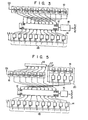
- Fig. 3 shows a circuit diagram of a DA converter according to the first embodiment of the present invention.
- the DA converter of this embodiment has a 10-bit binary counter 10 of up-counter type which receives clock pulses CK of a predetermined frequency, a comparator 12 which compares two binary numbers and produces an output representing which one of the two binary numbers is greater or smaller, a 10-bit register 14 for temporarily storing 10-bit digital data DD to be converted, and a smoothing circuit 15 comprising, for example, a low-pass filter for smoothing the pulse signals generated by the comparator 12.
- the 10-bit binary counter 10 counts the received clock pulses CK and generates a 10-bit binary number which is sequentially incremented.
- the lower six significant bits Q0, Ql,..., Q5 are applied to the upper six significant bits of the comparator 12 in this order whereas the upper four significant bits Q6 to Q9 are inverted in order and are applied to the lower four significant bits of the comparator 12.
- the binary number input to the comparator 12 may be given as:
- This binary number defines 2 4 binary number strings of 2 6 steps with one step corresponding to 2 4 (the binary number strings are indicated by staircase waves Il to I16). These binary number strings respectively have different weights (Q9 x 2 0 + Q8 x 2 1 + Q7 x 2 7 + Q6 x 2 3 ). These weights are shown in Table 1 below based upon the relations with bits Q6 to Q9.
- the values from the LSB to the fourth bit input to the comparator 12 are such that the orders of decimal numbers 0 to 15 are dispersed at maximum as shown in the right column of Table 1 above.
- the digital data DD to be converted is temporarily stored in the 10-bit register 14 and supplied to the comparator 12 in response to a load signal LA.
- the comparator 12 sequentially compares the digital data DD with the binary number strings supplied from the binary counter 10 and produces the comparison outputs. Some comparison outputs produced by the comparator 12 differ by one step from other comparison outputs according to the weights of the binary number strings to be compared with the digital data DD.
- the binary number string reaches the value of the digital data DD, 555, at the 34th step when the weight is 11. Therefore, the comparison outputs are produced by the comparator 12 within the range of 34 steps for the binary number string whose weight exceeds 11.
- the comparison outputs are produced by the comparator 12 within the range of (34 + 1) steps for the binary number string whose weight is 11 or less.
- the comparison outputs from the comparator 12 are produced in correspondence with (34 + 1), (34 + 1), (34 + 1), 34, (34 + 1), (34 + 1), (34 + 1), 34, (34 + 1), (34 + 1), (34 + 1), 34, (34 + 1) and 34 steps in the example shown in Table 1.
- weights with which outputs are obtained in correspondence with 34 steps are indicated with symbol o.
- most of the comparison outputs (pulse train) are produced by the comparator 12 over the range of 35 steps; the comparison output are produced over the range of 34 steps at the positions of maximum dispersion in this pulse train within the conversion period.
- the pulse widths only differ in correspondence with one step.
- the pulse train obtained in this manner is supplied to the smoothing circuit 15.
- the smoothing circuit 15 converts the PWM wave into a dc output from which the ripple components are effectively attenuated.
- a DA conversion of 555/2 10 per conversion period is obtained with high accuracy.
- a dc output signal close to an objective value is obtained per duration which is 1/16 the conversion period.
- a correction equivalent to the LSB of the data to be converted is of small fraction and effectively dispersed within one conversion period. Therefore, the conversion speed becomes faster than that of the conventional DA converters.
- the cut-off frequency of the smoothing circuit (low-pass filter) 15 for smoothing the PWM waves can be made nearly 16 times that with the conventional DA converter.
- the ripple components of the PWM waves can be effectively attenuated so that a dc output of good quality may be obtained.
- the weights of the binary number strings are generated within one period of the staircase wave.
- the present invention is not limited to this.
- similar effects may be obtained by generating the weights over a duration of two periods.
- the second embodiment of the present invention as shown in Fig. 5 achieves this.
- the same reference numerals in Fig. 5 as those in Fig. 3 denote the same parts.
- the DA converter of the second embodiment comprises a 6-bit binary counter 16 for receiving the clock pulse CK, a 4-bit binary counter 18, a latch circuit 20 for latching the output from the 4-bit binary counter 18, and a detection circuit 22 which supervises the count of the 6-bit binary counter 16 and which generates a count pulse CP for the 4-bit binary counter 18 and a latch pulse LP for the latch circuit 20.
- the staircase waves from the 6-bit binary counter 16 have the period as shown in Fig.
- a count pulse CP is generated by the detection circuit 22 after a fixed duration from the beginning of each staircase wave, as shown in Fig. 6(B), to increment the count of the 4-bit binary counter 18 by one.
- a latch pulse LP is generated after another fixed duration from the count pulse CP, as shown in Fig. 6(C), to latch the count of the 4-bit binary counter 18 in the latch circuit 20.
- the bits QO to Q5 of the output from the 6-bit binary counter 16 are directly supplied to the upper six significant bits of the 10-bit comparator 12, whereas the latched content in the latch circuit 20 is reversed in the order of bits and supplied to the lower four significant bits of the 10-bit comparator 12. Other details of the arrangement remain the same as those of the embodiment shown in Fig. 3.
- the weights of the respective staircase waves change when the latch pulses LP are generated by the detection circuit 22; all the weights are generated within one conversion period.
- the output data from the 4-bit binary counter 18 it suffices that the output data from the 4-bit binary counter 18 be established substantially within the period of each staircase wave. Therefore, the operation speed of the 4-bit binary counter 18 may be significantly lowered in comparison with that of the 6-bit binary counter 16.
- the second embodiment has an advantage in manufacture of the DA converter in addition to the advantages obtained with the first embodiment.
- F ig. 7 shows the third embodiment of the present invention.
- a 4-bit comparator 24 for comparing the lower four significant bits and a 6-bit comparator 26 for comparing the upper six significant bits are incorporated in place of the 10-bit comparator 12 shown in Fig. 5.
- the 4-bit comparator 24 first compares the inverted signal of the output signal from the 4-bit binary counter 18 with the lower four significant bits of the binary number to be converted.
- the comparison output from the 4-bit comparator 24 is latched in a latch circuit 28 in response to the latch pulse LP from the detection circuit 22.
- the latched content in the latch circuit 28 is supplied to the 6-bit comparator 26.
- the 6-bit comparator 26 has the priority for producing the comparison output over the 4-bit comparator 24, and the 6-bit comparator 26 receives the comparison output from the 4-bit comparator only when the data to be compared coincide with each other. Since the digital data DD to be converted within the conversion period remains constant, the weights of the respective staircase waves change when the latch pulses are generated by the detection circuit 22 as in the case of the second embodiment shown in Fig. 5. Therefore, the output PWM waves same as those obtainable with the second embodiment shown in Fig. 5 are obtained. In the third embodiment, the operation speeds of the 4-bit binary counter 18 and the 4-bit comparator 24 can be significantly lowered for the same reason as that described with reference to the second embodiment shown in Fig. 5. Thus, the third embodiment achieves the similar effects to those of the second embodiment.
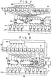
- F ig. 8 shows a DA converter according to the fourth embodiment of the present invention.
- the same reference numerals in Fig. 8 as those in Fig. 3 denote the same parts.
- the upper four significant bits of the count of the 10-bit binary counter 10 are reversed in the order of bits and are supplied to a 4-bit comparator 30. More specifically, when the upper four significant bits of the count of the 10-bit binary counter 10 are denoted by Q6 to Q9, the most significant bit (to be referred to as MSB hereinafter) Q9 is input to the LSB of the 4-bit comparator 30. The subsequent bits Q8 and Q7 are input to the second and third bits of the 4-bit comparator 30. The bit Q6 is input to the MSB of the comparator 30. The lower six significant bits of the count of the 10-bit binary counter 10 are directly supplied to a 6-bit coincidence circuit 32.
- the LSB QO is supplied to the LSB of the 6-bit coincidence circuit 32.
- the bits Ql to Q4 are supplied to the second to fourth bits, and the bit Q5 is supplied to the MSB of the coincidence circuit 32.
- the lower four significant bits of the input digital data DD to be converted are also input, as a comparison input, to the 4-bit comparator 30.
- the comparator 30 compares the value (value A) of the lower four bits of the digital data DD with the value (value B) output from the 10-bit binary counter 10.
- the comparator 30 outputs a signal "0" if A > B while it outputs a signal "1” if A > B.
- the signal "0" or "1" output from the comparator 30 is supplied to a delay control circuit 34.
- the upper six significant bits of the input digital data DD to be converted are also supplied to the 6-bit coincidence circuit 32.
- the coincidence circuit 32 compares the value (value C) of the upper six significant bits with the value (value D) from the binary counter 10.
- the signal "0" or “1” generated from the coincidence circuit 32 is supplied to the delay control circuit 34.
- the delay control circuit 34 comprises a D flip-flop 36, AND circuits 38 and 40 each having two input ends, an inverter 42, and an OR circuit 44. If the output signal from the comprator 30 is 111" (A ⁇ B), the output signal from the coincidence circuit 32 is directly output, that is, without delay.
- the output signal from the comparator 30 is "0" (A > B)
- the output signal from the coincidence circuit 32 is output as delayed by a duration corresponding to one period of the clock pulse CK (to be referred to as one clock time hereinafter).
- the AND circuit 40 is rendered operative to produce the output signal from the coincidence circuit 32 through the AND circuit 40 and the OR circuit 44.
- the AND circuit 38 is rendered operative in response to a signal input thereto through the inverter 42.
- the output signal from the coincidence circuit 32 is delayed by one clock time by the D flip-flop 36 and is then output through the AND circuit 38 and the OR circuit 44.
- the clock pulse CK is input as a drive pulse to the D flip-flop 36.
- the output from the coincidence circuit 32 supplied to a data input terminal D of the D flip-flop 36 is output as delayed by one clock time.
- the output from the delay control circuit 34 is supplied to a reset input R of an SR flip-flop 46.
- the output from a detection circuit 48 is supplied to a set input S of the SR flip-flop 46.
- the comparator 30 Since the upper four significant bits Q6 to Q9 from the binary counter 1 are inverted in the order of bits and are input to the comparator 30, the comparator 30 receives a binary number Q 9 x 2 0 + Q 8 x 2 1 + Q7 x 2 2 + Q6 x 2 3 .
- the bits Q6 to Q9 output from the binary counter 10 and the values input to the comparator 30 correspond in the manner as shown in Table 1 above.
- substantially equal 16 pulse trains having a duty of 3 4/2 6 or 3 5/2 6 within the conversion period are obtained as shown in Figs. 4(A) and 4(B) as in the case of the first embodiment.
- the pulses having a duty of 34/2 6 are obtained as maximally dispersed among pulses having a duty of 34/2 6 . Therefore, the fourth embodiment has the similar effects to those obtainable with the first embodiment.
- Fig. 9 shows a circuit diagram of the fifth embodiment of the present invention.
- the same reference numerals as in Figs. 5 and 8 denote the same parts.
- the fifth embodiment shown in Fig. 9 differs from the first embodiment in the following respects.
- the 6-bit binary counter 16, the 4-bit binary counter 18 and the latch circuit 20 are incorporated in place of the 10-bit binary counter 10.
- the 4-bit binary counter 18 is rendered operative in response to the output (count pulse CP) from a detection circuit 50 which detects if the count of the 6-bit binary counter 16 has reached a predetermined value.
- the count of the 4-bit binary counter 18 is latched by the latch circuit 20 in response to the output (latch pulse LP) from the detection circuit 50 and is then supplied to the comparator 30.
- the other configuration remains the same. With the embodiment of this configuration, the operation speed of the 4-bit binary counter 18 can be made significantly lower than that of the 6-bit binary counter 16.
- the signal supplied to the comparator remains constant for a duration corresponding to one period of the staircase wave. Therefore, the operation speed of the 4-bit binary counter 18 can be significantly lowered if the count pulse CP for rendering the 4-bit binary counter 18 operative is supplied thereto during the initial period of the staircase wave, and if the count of the 4-bit binary counter 18 is latched in the latch circuit 20 and is supplied to the comparator 30 after the counting operation of the 4-bit binary counter 18 is completed, as shown in Figs. 10(A), 10(B) and 10(C). In Figs. 10(A), 10(B) and 10(C), the latch pulse LP is generated in synchronism with the leading edge of the staircase wave.
- the latch pulse LP need not be generated in synchronism with the leading edge or the trailing edge of the staircase.
- the latch pulse LP may be generated at the timing as shown in Figs. 6(A), 6(B) and 6(C).
- the timing for generating the latch pulse LP may be arbitrarily set. Accordingly, the fifth embodiment provides the same effects as the second embodiment.
- Fig. 11 shows the sixth embodiment of the present invention.
- the latch circuit 28 is connected to the output end of the comparator 30 in place of the latch circuit 20 of the fifth embodiment shown in Fig. 9.
- the output from the comparator 30 is latched in the latch circuit 28 in synchronism with the latch pulse LP output from the detection circuit 50 and is supplied to the delay control circuit 34.
- the mode of operation of the sixth embodiment is basically the same as that of the fifth embodiment shown in Fig. 9, the operation speeds of the 4-bit binary counter 18 and the comparator 30 may be significantly lowered by suitably selecting the timings at which the count pulse CP to be supplied to the 4-bit binary counter 18 and the latch pulse LP to be supplied to the latch circuit 28 are generated. In this manner, the sixth embodiment also provides the same effects as the second embodiment.
- the present invention is not limited to the first to sixth embodiments described above.
- the present invention is applied to a 10-bit PWM-type DA converter.
- the present invention can be applied to PWM-type DA converters having any number of bits.
- the number of bits of each staircase wave-and the number of bits of the weight were divided into four and six bits. These bits may be divided in many ways depending upon the purpose.
- the binary counters comprise up- counters. Therefore, the sawtooth waves were generated as the staincase waves. However, if the binary counters comprise up-down counters, the staircase waves of triangular shape may be obtained. A DA converter of similar effects may be obtained in this case.
- the binary counters may comprise down-counters or synchronous counters.
- the coincidence output signal from the coincidence circuit 32 may be input to the D flip-flop 36. And the signal delayed by one clock time in response to the clock pulse CK may be supplied to the D input of the D flip-flop 36 and to the input end of the AND circuit 40. In this manner, the error due to logic delay of the coincidence circuit 32 may be reduced.
Landscapes
- Engineering & Computer Science (AREA)
- Theoretical Computer Science (AREA)
- Analogue/Digital Conversion (AREA)
Applications Claiming Priority (4)
| Application Number | Priority Date | Filing Date | Title |
|---|---|---|---|
| JP56040494A JPS57155833A (en) | 1981-03-23 | 1981-03-23 | Digital-to-analog converting circuit |
| JP40494/81 | 1981-03-23 | ||
| JP40495/81 | 1981-03-23 | ||
| JP56040495A JPS57155834A (en) | 1981-03-23 | 1981-03-23 | Digital-to-analog converting circuit |
Publications (3)
| Publication Number | Publication Date |
|---|---|
| EP0061292A2 true EP0061292A2 (de) | 1982-09-29 |
| EP0061292A3 EP0061292A3 (en) | 1983-09-14 |
| EP0061292B1 EP0061292B1 (de) | 1986-06-18 |
Family
ID=26379956
Family Applications (1)
| Application Number | Title | Priority Date | Filing Date |
|---|---|---|---|
| EP82301357A Expired EP0061292B1 (de) | 1981-03-23 | 1982-03-17 | Digital-Analog-Umwandler |
Country Status (3)
| Country | Link |
|---|---|
| US (1) | US4532496A (de) |
| EP (1) | EP0061292B1 (de) |
| DE (1) | DE3271734D1 (de) |
Cited By (2)
| Publication number | Priority date | Publication date | Assignee | Title |
|---|---|---|---|---|
| EP0509484A1 (de) * | 1991-04-17 | 1992-10-21 | Rohm Co., Ltd. | Pulsbreiten-Modulationschaltung für die Ansteuerung eines Kreuzspulanzeigeinstrumentes |
| WO2000035095A1 (en) * | 1998-12-04 | 2000-06-15 | Koninklijke Philips Electronics N.V. | Pulse density modulation based digital-to-analog conversion |
Families Citing this family (6)
| Publication number | Priority date | Publication date | Assignee | Title |
|---|---|---|---|---|
| US5198818A (en) * | 1991-11-07 | 1993-03-30 | Pairgain Technologies, Inc. | Oversampled digital-to-analog converter for multilevel data transmission |
| US5764165A (en) * | 1996-05-03 | 1998-06-09 | Quantum Corporation | Rotated counter bit pulse width modulated digital to analog converter |
| KR100220383B1 (ko) * | 1996-07-09 | 1999-09-15 | 윤종용 | Pwm을 이용한 디지탈/아날로그 변환장치 및 그 변환방법 |
| US6191722B1 (en) | 1999-01-14 | 2001-02-20 | Setra Systems, Inc. | Pulse width modulation digital to analog converter |
| US6525501B1 (en) * | 2000-05-26 | 2003-02-25 | Motorola | Method and apparatus for accelerating communication between controllable devices |
| JP4125032B2 (ja) * | 2002-04-12 | 2008-07-23 | キヤノン株式会社 | レーザ制御装置及び画像形成装置 |
Family Cites Families (4)
| Publication number | Priority date | Publication date | Assignee | Title |
|---|---|---|---|---|
| DE2317851B2 (de) * | 1973-04-10 | 1975-04-24 | Grundig E.M.V. Elektro-Mechanische Versuchsanstalt Max Grundig, 8510 Fuerth | Digital-Analog-Wandler |
| US4096475A (en) * | 1975-04-08 | 1978-06-20 | U.S. Philips Corporation | Circuit for the conversion of a digital signal to an analog signal |
| JPS5228205A (en) * | 1975-08-28 | 1977-03-03 | Sony Corp | Station selector unit |
| JPS547263A (en) * | 1977-06-20 | 1979-01-19 | Hitachi Ltd | D-a converter |
-
1982
- 1982-03-17 EP EP82301357A patent/EP0061292B1/de not_active Expired
- 1982-03-17 DE DE8282301357T patent/DE3271734D1/de not_active Expired
-
1984
- 1984-06-26 US US06/624,747 patent/US4532496A/en not_active Expired - Lifetime
Cited By (3)
| Publication number | Priority date | Publication date | Assignee | Title |
|---|---|---|---|---|
| EP0509484A1 (de) * | 1991-04-17 | 1992-10-21 | Rohm Co., Ltd. | Pulsbreiten-Modulationschaltung für die Ansteuerung eines Kreuzspulanzeigeinstrumentes |
| US5291126A (en) * | 1991-04-17 | 1994-03-01 | Rohm Co., Ltd. | Pulse width modulation driving circuit for a cross coil meter |
| WO2000035095A1 (en) * | 1998-12-04 | 2000-06-15 | Koninklijke Philips Electronics N.V. | Pulse density modulation based digital-to-analog conversion |
Also Published As
| Publication number | Publication date |
|---|---|
| DE3271734D1 (de) | 1986-07-24 |
| US4532496A (en) | 1985-07-30 |
| EP0061292A3 (en) | 1983-09-14 |
| EP0061292B1 (de) | 1986-06-18 |
Similar Documents
| Publication | Publication Date | Title |
|---|---|---|
| US5337338A (en) | Pulse density modulation circuit (parallel to serial) comparing in a nonsequential bit order | |
| US4703308A (en) | Apparatus and methods for digital-to-analogue conversion | |
| US3836908A (en) | Digital to analog converter | |
| US4590457A (en) | Digital to analog converter utilizing pulse width modulation | |
| CA2004317C (en) | Successive comparison type analog-to-digital converting apparatus | |
| JP4073676B2 (ja) | Da変換器及びda変換方法 | |
| JPS6143899B2 (de) | ||
| EP0492434A2 (de) | Verfahren zur Konversion eines digitalen Signals in ein analoges Signals in einem Digital/Analog-Wandler | |
| EP0061292A2 (de) | Digital-Analog-Umwandler | |
| US4467319A (en) | Signal conversion circuit | |
| CN1046607A (zh) | 用于精确数字测定信号脉冲序列的时间或相位位置的方法和装置 | |
| GB2089606A (en) | Analog-to-digital converter circuits | |
| US6169504B1 (en) | Device and method for converting analog signal to digital signal using interleaving sampling | |
| US5812831A (en) | Method and apparatus for pulse width modulation | |
| US4144525A (en) | Cascadable analog to digital converter | |
| US4636773A (en) | Binarily weighted pulse width digital-to-analog converter | |
| JPS6359570B2 (de) | ||
| JPH0787376B2 (ja) | デルタ変調符号の復号装置 | |
| JPH02184119A (ja) | オーバーサンプリング形デジタル―アナログ変換回路 | |
| US5502440A (en) | Structure and method for performing analog to digital conversion | |
| JPS6352808B2 (de) | ||
| JPH0653794A (ja) | パルス幅変調回路 | |
| JPS6013335B2 (ja) | デイジタル・アナログ変換器 | |
| US5053729A (en) | Pulse-width modulator | |
| JPS6022681Y2 (ja) | ディジタル・アナログ変換器 |
Legal Events
| Date | Code | Title | Description |
|---|---|---|---|
| PUAI | Public reference made under article 153(3) epc to a published international application that has entered the european phase |
Free format text: ORIGINAL CODE: 0009012 |
|
| 17P | Request for examination filed |
Effective date: 19820329 |
|
| AK | Designated contracting states |
Designated state(s): DE FR GB NL |
|
| PUAL | Search report despatched |
Free format text: ORIGINAL CODE: 0009013 |
|
| AK | Designated contracting states |
Designated state(s): DE FR GB NL |
|
| RAP1 | Party data changed (applicant data changed or rights of an application transferred) |
Owner name: KABUSHIKI KAISHA TOSHIBA |
|
| GRAA | (expected) grant |
Free format text: ORIGINAL CODE: 0009210 |
|
| AK | Designated contracting states |
Kind code of ref document: B1 Designated state(s): DE FR GB NL |
|
| REF | Corresponds to: |
Ref document number: 3271734 Country of ref document: DE Date of ref document: 19860724 |
|
| ET | Fr: translation filed | ||
| PLBE | No opposition filed within time limit |
Free format text: ORIGINAL CODE: 0009261 |
|
| STAA | Information on the status of an ep patent application or granted ep patent |
Free format text: STATUS: NO OPPOSITION FILED WITHIN TIME LIMIT |
|
| 26N | No opposition filed | ||
| PGFP | Annual fee paid to national office [announced via postgrant information from national office to epo] |
Ref country code: DE Payment date: 19970321 Year of fee payment: 16 |
|
| PGFP | Annual fee paid to national office [announced via postgrant information from national office to epo] |
Ref country code: GB Payment date: 19980309 Year of fee payment: 17 |
|
| PGFP | Annual fee paid to national office [announced via postgrant information from national office to epo] |
Ref country code: FR Payment date: 19980310 Year of fee payment: 17 |
|
| PGFP | Annual fee paid to national office [announced via postgrant information from national office to epo] |
Ref country code: NL Payment date: 19980326 Year of fee payment: 17 |
|
| PG25 | Lapsed in a contracting state [announced via postgrant information from national office to epo] |
Ref country code: DE Free format text: LAPSE BECAUSE OF NON-PAYMENT OF DUE FEES Effective date: 19981201 |
|
| PG25 | Lapsed in a contracting state [announced via postgrant information from national office to epo] |
Ref country code: GB Free format text: LAPSE BECAUSE OF NON-PAYMENT OF DUE FEES Effective date: 19990317 |
|
| PG25 | Lapsed in a contracting state [announced via postgrant information from national office to epo] |
Ref country code: NL Free format text: LAPSE BECAUSE OF NON-PAYMENT OF DUE FEES Effective date: 19991001 |
|
| GBPC | Gb: european patent ceased through non-payment of renewal fee |
Effective date: 19990317 |
|
| PG25 | Lapsed in a contracting state [announced via postgrant information from national office to epo] |
Ref country code: FR Free format text: LAPSE BECAUSE OF NON-PAYMENT OF DUE FEES Effective date: 19991130 |
|
| NLV4 | Nl: lapsed or anulled due to non-payment of the annual fee |
Effective date: 19991001 |
|
| REG | Reference to a national code |
Ref country code: FR Ref legal event code: ST |