EP0061377A1 - Digitaler Signaldemodulator und einen derartigen Demodulator enthaltender Farbfernsehempfänger oder -system - Google Patents
Digitaler Signaldemodulator und einen derartigen Demodulator enthaltender Farbfernsehempfänger oder -system Download PDFInfo
- Publication number
- EP0061377A1 EP0061377A1 EP82400389A EP82400389A EP0061377A1 EP 0061377 A1 EP0061377 A1 EP 0061377A1 EP 82400389 A EP82400389 A EP 82400389A EP 82400389 A EP82400389 A EP 82400389A EP 0061377 A1 EP0061377 A1 EP 0061377A1
- Authority
- EP
- European Patent Office
- Prior art keywords
- signal
- vector
- output
- phase
- frequency
- Prior art date
- Legal status (The legal status is an assumption and is not a legal conclusion. Google has not performed a legal analysis and makes no representation as to the accuracy of the status listed.)
- Granted
Links
- 239000013598 vector Substances 0.000 claims abstract description 42
- 238000005070 sampling Methods 0.000 claims abstract description 9
- 239000000969 carrier Substances 0.000 claims abstract description 8
- 238000004364 calculation method Methods 0.000 claims description 41
- 230000015654 memory Effects 0.000 claims description 14
- 230000006870 function Effects 0.000 claims description 8
- 239000002131 composite material Substances 0.000 claims description 2
- 230000010363 phase shift Effects 0.000 claims description 2
- 230000001629 suppression Effects 0.000 abstract description 2
- 238000000034 method Methods 0.000 description 17
- 230000014509 gene expression Effects 0.000 description 12
- 230000001934 delay Effects 0.000 description 2
- 230000005540 biological transmission Effects 0.000 description 1
- 230000008030 elimination Effects 0.000 description 1
- 238000003379 elimination reaction Methods 0.000 description 1
- 230000010349 pulsation Effects 0.000 description 1
- 230000033764 rhythmic process Effects 0.000 description 1
- 238000001228 spectrum Methods 0.000 description 1
Images
Classifications
-
- H—ELECTRICITY
- H03—ELECTRONIC CIRCUITRY
- H03D—DEMODULATION OR TRANSFERENCE OF MODULATION FROM ONE CARRIER TO ANOTHER
- H03D3/00—Demodulation of angle-, frequency- or phase- modulated oscillations
- H03D3/006—Demodulation of angle-, frequency- or phase- modulated oscillations by sampling the oscillations and further processing the samples, e.g. by computing techniques
-
- H—ELECTRICITY
- H04—ELECTRIC COMMUNICATION TECHNIQUE
- H04N—PICTORIAL COMMUNICATION, e.g. TELEVISION
- H04N9/00—Details of colour television systems
- H04N9/64—Circuits for processing colour signals
- H04N9/642—Multi-standard receivers
-
- H—ELECTRICITY
- H03—ELECTRONIC CIRCUITRY
- H03D—DEMODULATION OR TRANSFERENCE OF MODULATION FROM ONE CARRIER TO ANOTHER
- H03D2200/00—Indexing scheme relating to details of demodulation or transference of modulation from one carrier to another covered by H03D
- H03D2200/0041—Functional aspects of demodulators
- H03D2200/005—Analog to digital conversion
-
- H—ELECTRICITY
- H03—ELECTRONIC CIRCUITRY
- H03D—DEMODULATION OR TRANSFERENCE OF MODULATION FROM ONE CARRIER TO ANOTHER
- H03D2200/00—Indexing scheme relating to details of demodulation or transference of modulation from one carrier to another covered by H03D
- H03D2200/0041—Functional aspects of demodulators
- H03D2200/006—Signal sampling
- H03D2200/0062—Computation of input samples, e.g. successive samples
Definitions
- the present invention relates to digital demodulators making it possible to demodulate on the one hand, a frequency modulated signal, for example a chrominance signal of a SECAM video frequency signal, and on the other hand an amplitude modulated signal resulting from a modulation in amplitude, with suppressed carrier, of two carriers in phase quadrature, for example a chrominance signal of a PAL video signal.
- a frequency modulated signal for example a chrominance signal of a SECAM video frequency signal
- an amplitude modulated signal resulting from a modulation in amplitude, with suppressed carrier, of two carriers in phase quadrature for example a chrominance signal of a PAL video signal.
- the present invention further relates to color television receivers and systems comprising such devices, in particular PAL / SECAM color television receivers and systems.
- receiver will be understood here any display device on the screen of a three-color cathode ray tube, of a color image obtained from a video or composite video signal comprising a frequency modulated carrier of the SECAM system or two carriers in amplitude modulated phase quadrature transmitted with suppression of the carrier frequency outside the rear horizontal synchronization steps of the PAL system, such as a monitor or a color television receiver.
- SECAM demodulator a demodulator of a frequency modulated signal
- the principle implemented by the demodulator described in the aforementioned second publication consists in sampling the signal, in determining the polar coordinates of the rotating vector representative of the signal by means of two successive samples of the signal to be demodulated, and in calculating the values of the amplitudes of the two modulation signals in. function of the polar coordinates of the rotating vector and of the instants at which the signal to be demodulated is sampled.
- PAL / SECAM television systems it is known to produce a PAL / SECAM digital demodulator which includes a demodulator.
- PAL. and a SECAM demodulator such as those cited in the prior art.
- Such an embodiment implements a completely independent PAL demodulation method and a SECAM demodulation method.
- the present invention relates to a digital PAL / SECAM demodulator which is much simpler than that obtained using the PAL and SECAM demodulators of the prior art. This simplicity is due to an implementation of a SECAM demodulation method and of a PAL demodulation method having common parts, which. leads to a reduction in the number of circuits necessary for producing the demodulator.
- a digital demodulator allowing the demodulation either of a signal x S (t) modulated in frequency around a frequency F, or of a signal xp (t) modulated in amplitude resulting from an amplitude modulation , with carrier removed, two carriers at the same frequency F and in phase quadrature by two modulation signals, is characterized in that it comprises: a sampler of the signal to be demodulated according to the sampling frequency 4F; an analog-to-digital converter of the samples selected by the sampler; a first delay device, with delay e equal to , having an input coupled to the output of the converter; a second delay device, delay ⁇ 1 , having an input coupled to the output of the first delay device; a device for determining the module and the phase of the vector Z (t) representative of the signal to be demodulated having first, second and third inputs respectively coupled to the output of the converter, to the output of the first delay device and of the second device to delay, first calculation means determining the frequency variation of the signal
- a receiver and a television system comprising such a demodulator.
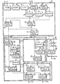
- the exemplary embodiment described in this figure makes it possible to demodulate either a chrominance signal of a SECAM video signal, or a chrominance signal of a PAL video signal.
- a SECAM chrominance signal is frequency modulated around a subcarrier in the vicinity of 4.3 MHz and has a frequency spectrum ranging from 3.9 MHz to 4.7 MHz,. and that a PAL chrominance signal results from a modulation in amplitude of two subcarriers of the same frequency equal to 4.4 MHz, but phase shifted relative to each other by 90 °.
- the demodulator according to the invention consists of three distinct parts A, B and C, an input terminal 1 intended to receive either a PAL video signal or a SECAM video signal, an output terminal 29 used during demodulation of a SECAM chrominance signal, and of two output terminals 25 and 26 used during demodulation of a PAL chrominance signal.
- Parts A and B constitute a SECAM demodulator implementing a demodulation method which differs from the method described in the prior art by the way of determining the position of the rotating vector (part A).
- Parts A and C constitute a PAL demodulator having a part A common with the SECAM demodulator.
- This PAL demodulator implements a demodulation method which differs from the method described in the prior art by the way of determining the polar coordinates of the rotating vector (part A).
- this PAL / SECAM demodulator is to use on the one hand a SECAM demodulator (parts A and B) in which the determination of the position of the rotating vector is carried out using linear combinations of determined samples and judiciously chosen, and on the other hand a PAL demodulator (parts A and C) in which the determination of the polar coordinates of the rotating vector is carried out using the same linear combinations as those used by the SECAM demodulator.
- Demodulating a chrominance signal from a SECAM videofrequency signal amounts to determining the frequency of a sinusoid varying in a 0.8 MHz frequency band B centered around the frequency F equal to 4.3 MHz. It can be considered that this sinusoid is obtained by the projection x S (t), on an axis Ox of an orthogonal coordinate system Oxy, of a rotating vector Z S (t) around the origin O to the angular velocity 2 ⁇ (F + ⁇ F), ⁇ F being the value of the frequency excursion and t representing time.
- the equation of x S (t) is given by:
- x S (t) Let three values of x S (t) be obtained at regular time intervals equal to , for example x S (t 1 ), x S (t 1 - ) and x S (t 1 - ), t 1 being any moment.
- the SECAM calculation method which has just been explained has the advantage of determining the position of the rotating vector (i.e. '(t 1 )) using a cosine arc simpler to implement than the tangent arc calculation of the prior art. Another advantage of this calculation method is that it can be used during demodulation of a PAL chrominance signal.
- the demodulation method implemented by the PAL demodulator cited in the prior art can be applied by taking as polar coordinates of the rotating vector R and '(t 1 ) calculated according to the SECAM calculation method.
- cos ⁇ t and sin ⁇ t respectively correspond to the first subcarrier and to the second subcarrier with the same pulsation and phase shifted by 90 ° relative to each other.
- a (t) and B (t) correspond to the amplitude modulation signals of the two subcarriers.
- Demodulating a signal whose amplitude is given by the expression 6 amounts to determining the values of ⁇ and ⁇ .
- the polar coordinates ( ⁇ t ⁇ t ) of the vector Z P (t 1 ) can be calculated using the following formulas:
- the formula 8 does not allow direct deduction of arc tg . Indeed, the term wt 1 depends on the initial sampling instant.
- C represents a constant
- ⁇ o corresponds to the phase shift between the reference burst and the first subcarrier.
- the value of ⁇ o is 135 °.
- the demodulation method which has just been described consists in sampling on the one hand the reference burst and on the other hand the chrominance signal at a rhythm equal to 4 times the frequency F of the subcarrier, at store each sample for a period of time in order to have at each instant three successive samples, to calculate the polar coordinates of the vectors associated with the reference burst and the chrominance signal (formulas 7, 8, 9 and 10), to determine the value of y from the formula 11, and finally to calculate the values of a and ⁇ according to the equations 12 and 13.
- Part A of the demodulator corresponds to the circuits implementing the calculation method common to the two demodulation methods described above.
- This part A has an input connected to the input terminal 1, a first output 31 providing either R, or ⁇ t , or ⁇ and a second output 32 providing either '(t 1 ), either ⁇ t 1 or ⁇ depending on the type of signal present on input terminal 1.
- the video signal received on the input terminal 1 is filtered by a filter 2 to select only the chrominance signal.
- This filter is a bandpass.
- the signal obtained at the output of filter 2 is sampled, from an initial instant t o , by a sample 3 according to the sampling frequency 4F.
- the samples are then converted into binary signals by an analog-digital converter 4.
- Another delay device 6 delays the samples supplied by the delay device 5 by a duration T.
- a register 7 whose input is connected to the output of the converter 4, a register 8 whose input is connected to the output of the delay device 5 and a register 9 whose input is connected to the output of the delay device 6 are actuated at frequency F and allow, at any time t 1 , to have simultaneously three successive samples: X (t 1 ), X (t 1 - ) and X (t 1 - ).
- a calculation device 10 of which a first and a second input are respectively connected to the output of register 7 and to the output of register 9, makes it possible to calculate A computing device 11 including a first and a second input are respectively connected to the output of the register 8 and to the output of the calculation device 10, allows to calculate Y 2 (t 1 ) + X 2 (t 1 - ).
- the calculation devices 11 and 12 respectively supply R (formula 1 and ⁇ '(t 1 ) (formula 2).
- the computing devices 11 and 12 respectively provide ⁇ t (formula 7 and ⁇ t 1 (formula 8.
- these computing devices 11 and 12 respectively provide ⁇ and ⁇ (formulas 9 and 10).
- Part B of the demodulator according to the invention consists of a delay device 27 whose input is connected to the output of the computing device 12 and of a computing device 28 of which a first and a second input are respectively connected at the output of the computing device 12 and at the output of the delay device 27 and the output of which is connected to the output terminal 29.
- the delay generated by the delay device 27 is .
- the calculation device 28 makes it possible to calculate according to the formula 3 the frequency variation ⁇ F between two instants distant by 1 F.
- Part B of the demodulator can only be used for demodulating a SECAM chrominance signal.
- part C of the demodulator is used. This part C implements the calculation method explained above from the values ⁇ t1 , ⁇ t1 , ⁇ and ⁇ generated by the calculation devices 11 and 12.
- This part C has three subparts C 1 , C 2 and C 3 .
- Subpart C 1 makes it possible to calculate arc tg according to formula 11.
- this subpart C 1 includes a m moire 13 having a main input connected to the output of the computing device 12, a computing device 14 whose main input is connected to the output of the memory 13 and a subtraction circuit 15 of which a first and a second input are respectively connected to the output of the computing device 12 and to the output of the computing device 14.
- the memory 13 receives on an auxiliary input 40 a storage control signal S 1 indicating the presence of the reference burst. This memory 13 therefore stores the value of ⁇ associated with the reference burst. At the end of the reference burst, the memory 13 supplies the value of ⁇ to the calculation device 14.
- This calculation device 14 receives on another auxiliary input 41 the value of ⁇ o and calculates ⁇ - ⁇ o .
- the calculation device 15 calculates ⁇ - ⁇ t1 - ⁇ o , that is to say ⁇ (formula 11).
- Subpart C 2 makes it possible to calculate the real value of ⁇ t1 .
- the value provided by the calculation device 11 is in fact a being a variable variable in time, depending on the video frequency source and the transmission channel.
- the sub-part C 2 comprises a delay device 18, two memories 19 and 21, a subtraction circuit 20 and a multiplication circuit 22.
- This subpart C 2 The principle of calculation implemented by this subpart C 2 consists in comparing the value of the module ⁇ calculated during the presence of the reference burst with the theoretical value of this module. From this comparison, the coefficient a can be deduced. This coefficient a is then used to correct the values of the module P t associated with the chrominance signal PAL.
- the delay device 18, the input of which is connected to the output of the calculation device 11 generates a delay which corresponds to the difference in the time necessary for calculating the module and that necessary for calculating the phase.
- the memory 19 whose main input is connected to the output of the delay device 18 receives on an auxiliary input 42 a storage control signal S 2 indicating the presence of the reference burst. This memory 19 therefore stores the value ⁇ of the module associated with the reference burst.
- the subtraction circuit 20 comprises a first input connected to the output of the memory 19 and a second input 43 receiving the theoretical value ⁇ th of the module associated with the reference burst. The subtraction circuit 20 calculates the difference between and ⁇ th .
- Subpart C 3 comprises two calculation devices 16 and 17 and two multiplication circuits 23 and 24, and makes it possible to calculate ⁇ and ⁇ according to the formulas 12 and 13.
- the input of the computing device 17 and the input of the computing device 16 are connected to the output of the subtraction circuit 15 which delivers the value.
- the calculation device 16 calculates sin y.
- a first input of the multiplication circuit 23 and a first input of the multiplication circuit 24 are connected to the output of the multiplication circuit 22 which delivers the corrected values ⁇ t1 .
- the second input of the multiplication circuit 23 is connected to the output of the computing device 17.
- the second input of the multiplication circuit 24 is connected to the output of the computing device 16.
- the multiplication circuits 23 and 24 respectively calculate a and ⁇ according to formulas 12 and 13 and deliver these values to the output terminals 25 and 26.
- DTC charge transfer devices
- the invention is not only applicable for demodulating a PAL or SECAM chrominance signal, but can be used for demodulating any frequency modulated signal and any signal resulting from amplitude modulation, with suppressed carrier, of two carriers at the same frequency F and in phase quadrature (such as the chrominance signals of the NTSC system, for example).
Landscapes
- Engineering & Computer Science (AREA)
- Multimedia (AREA)
- Signal Processing (AREA)
- Theoretical Computer Science (AREA)
- Power Engineering (AREA)
- Processing Of Color Television Signals (AREA)
- Color Television Systems (AREA)
Applications Claiming Priority (2)
| Application Number | Priority Date | Filing Date | Title |
|---|---|---|---|
| FR8105285 | 1981-03-17 | ||
| FR8105285A FR2502423A1 (fr) | 1981-03-17 | 1981-03-17 | Demodulateur numerique de signaux et systeme de television comportant un tel demodulateur |
Publications (2)
| Publication Number | Publication Date |
|---|---|
| EP0061377A1 true EP0061377A1 (de) | 1982-09-29 |
| EP0061377B1 EP0061377B1 (de) | 1985-09-11 |
Family
ID=9256315
Family Applications (1)
| Application Number | Title | Priority Date | Filing Date |
|---|---|---|---|
| EP19820400389 Expired EP0061377B1 (de) | 1981-03-17 | 1982-03-05 | Digitaler Signaldemodulator und einen derartigen Demodulator enthaltender Farbfernsehempfänger oder -system |
Country Status (5)
| Country | Link |
|---|---|
| EP (1) | EP0061377B1 (de) |
| JP (1) | JPH0244197B2 (de) |
| DE (1) | DE3266100D1 (de) |
| ES (1) | ES8303845A1 (de) |
| FR (1) | FR2502423A1 (de) |
Cited By (3)
| Publication number | Priority date | Publication date | Assignee | Title |
|---|---|---|---|---|
| EP0109966A1 (de) * | 1982-11-26 | 1984-06-13 | Deutsche ITT Industries GmbH | Schaltungsanordnung zur digitalen FM-Demodulation |
| FR2552598A1 (fr) * | 1983-09-23 | 1985-03-29 | Labo Electronique Physique | Procede et circuit de demodulation numerique d'un signal module en amplitude et recepteur de television equipe d'un tel circuit |
| FR2602928A1 (fr) * | 1986-08-07 | 1988-02-19 | Int Mobile Machines | Ensemble d'abonne pour telephonie numerique sans fil; modem et dispositifs divers (synthetiseur de frequence...) pour cet ensemble |
Families Citing this family (4)
| Publication number | Priority date | Publication date | Assignee | Title |
|---|---|---|---|---|
| US4547737A (en) * | 1983-07-29 | 1985-10-15 | Rca Corporation | Demodulator of sampled data FM signals from sets of four successive samples |
| JPS60185475A (ja) * | 1984-03-05 | 1985-09-20 | Alps Electric Co Ltd | 高周波変調回路 |
| US4675863A (en) | 1985-03-20 | 1987-06-23 | International Mobile Machines Corp. | Subscriber RF telephone system for providing multiple speech and/or data signals simultaneously over either a single or a plurality of RF channels |
| US5546383A (en) | 1993-09-30 | 1996-08-13 | Cooley; David M. | Modularly clustered radiotelephone system |
Citations (5)
| Publication number | Priority date | Publication date | Assignee | Title |
|---|---|---|---|---|
| FR1585253A (de) * | 1968-08-09 | 1970-01-16 | ||
| FR2065682A1 (de) * | 1969-09-05 | 1971-08-06 | Rca Corp | |
| US3952187A (en) * | 1975-06-27 | 1976-04-20 | Ford Motor Company | Circuit for transforming rectangular coordinates to polar coordinates |
| US4090145A (en) * | 1969-03-24 | 1978-05-16 | Webb Joseph A | Digital quadrature demodulator |
| FR2433756A1 (fr) * | 1978-07-29 | 1980-03-14 | Licentia Gmbh | Discriminateur de frequence numerique |
-
1981
- 1981-03-17 FR FR8105285A patent/FR2502423A1/fr active Granted
-
1982
- 1982-03-05 DE DE8282400389T patent/DE3266100D1/de not_active Expired
- 1982-03-05 EP EP19820400389 patent/EP0061377B1/de not_active Expired
- 1982-03-16 ES ES510461A patent/ES8303845A1/es not_active Expired
- 1982-03-17 JP JP57040951A patent/JPH0244197B2/ja not_active Expired - Lifetime
Patent Citations (5)
| Publication number | Priority date | Publication date | Assignee | Title |
|---|---|---|---|---|
| FR1585253A (de) * | 1968-08-09 | 1970-01-16 | ||
| US4090145A (en) * | 1969-03-24 | 1978-05-16 | Webb Joseph A | Digital quadrature demodulator |
| FR2065682A1 (de) * | 1969-09-05 | 1971-08-06 | Rca Corp | |
| US3952187A (en) * | 1975-06-27 | 1976-04-20 | Ford Motor Company | Circuit for transforming rectangular coordinates to polar coordinates |
| FR2433756A1 (fr) * | 1978-07-29 | 1980-03-14 | Licentia Gmbh | Discriminateur de frequence numerique |
Cited By (5)
| Publication number | Priority date | Publication date | Assignee | Title |
|---|---|---|---|---|
| EP0109966A1 (de) * | 1982-11-26 | 1984-06-13 | Deutsche ITT Industries GmbH | Schaltungsanordnung zur digitalen FM-Demodulation |
| FR2552598A1 (fr) * | 1983-09-23 | 1985-03-29 | Labo Electronique Physique | Procede et circuit de demodulation numerique d'un signal module en amplitude et recepteur de television equipe d'un tel circuit |
| EP0137553A3 (de) * | 1983-09-23 | 1985-06-12 | Laboratoires D'electronique Et De Physique Appliquee L.E.P. | |
| FR2602928A1 (fr) * | 1986-08-07 | 1988-02-19 | Int Mobile Machines | Ensemble d'abonne pour telephonie numerique sans fil; modem et dispositifs divers (synthetiseur de frequence...) pour cet ensemble |
| US5842137A (en) * | 1986-08-07 | 1998-11-24 | Interdigital Technology Corporation | Subscriber unit for wireless digital telephone system |
Also Published As
| Publication number | Publication date |
|---|---|
| DE3266100D1 (en) | 1985-10-17 |
| ES510461A0 (es) | 1983-02-01 |
| JPH0244197B2 (ja) | 1990-10-03 |
| EP0061377B1 (de) | 1985-09-11 |
| JPS581389A (ja) | 1983-01-06 |
| ES8303845A1 (es) | 1983-02-01 |
| FR2502423B1 (de) | 1983-04-29 |
| FR2502423A1 (fr) | 1982-09-24 |
Similar Documents
| Publication | Publication Date | Title |
|---|---|---|
| EP0037317B1 (de) | Verfahren zur Demodulation eines amplitudemodulierten Signals, Demodulator zur Ausführung dieses Verfahrens und Fernsehsystem mit einem solchen Demodulator | |
| EP0091167B1 (de) | Verfahren zur Frequenzkorrektur des lokalen Trägers im Empfänger eines Datenübertragungssystems und Empfänger unter Verwendung dieses Verfahrens | |
| EP0702866B1 (de) | SIGNALISATIONSPAKET FüR KOMMUNIKATIONSSYSTEM MIT MODULIERTER REFERENZ DIE EINEM ZEITABHAENGIGEN GESETZ FOLGT | |
| EP0178720A1 (de) | Einrichtung zum Empfang von digitalen Daten mit einer adaptiven Taktrückgewinnungsschaltung | |
| EP0048661B1 (de) | Demodulator eines frequenzmodulierten Signals | |
| FR2550030A1 (fr) | Procede et dispositif pour la demodulation de la modulation de frequence | |
| FR2615675A1 (fr) | Procede de demodulation de signaux modules numeriquement et dispositif de mise en oeuvre d'un tel procede | |
| FR2731853A1 (fr) | Procede et dispositif de demodulation par echantillonnage, notamment pour systeme d'alarme de vehicule automobile | |
| FR2904168A1 (fr) | Systeme d'estimation de la qualite de reception d'une transmission numerique. | |
| EP0166839A1 (de) | Verfahren und Vorrichtung zur Messung des Phasen-Jitters eines Übertragungskanals | |
| FR2770700A1 (fr) | Dispositif et procede pour synchroniser des oscillateurs dans un systeme de communication de donnees | |
| EP0004822A1 (de) | Verfahren und Anordnung zur Demodulation eines in Differenzphasenumtastung dargestellten Signals | |
| EP0017716A1 (de) | Verfahren zur Anfangseinstellung eines adaptiven Entzerrers ausgehend von einem unbekannten Datensignal in einem Übertragungssystem mit Doppelseitenbandmodulation und Quadraturträgern | |
| EP0061377B1 (de) | Digitaler Signaldemodulator und einen derartigen Demodulator enthaltender Farbfernsehempfänger oder -system | |
| JPH09162940A (ja) | ダイレクトシーケンススペクトル拡散受信器用の信号品質評価方法 | |
| EP0029376B1 (de) | Verfahren zur Demodulation eines frequenzmodulierten Signals und Demodulator zur Durchführung des Verfahrens | |
| FR2623352A1 (de) | ||
| EP1330091B1 (de) | Verfahren zur Selektion einer Position eines FFT-Fensters in einem COFDM-Empfänger | |
| EP0046103B1 (de) | Verfahren zur Demodulation eines frequenzmodulierten Signals und Demodulator zur Durchführung des Verfahrens | |
| EP0107884A1 (de) | Digitale Messanordnung für die augenblickliche Frequenz eines frequenzmodulierten oder unmodulierten Signals sowie Fernseh- oder Rundfunkempfänger, der mit einer solchen Anordnung ausgerüstet ist | |
| FR2505111A1 (fr) | Dispositif de recuperation de porteuse pour une modulation d'amplitude et de phase a seize etats et systeme de reception de donnees numeriques comprenant un tel dispositif | |
| EP0080544B1 (de) | Verfahren zum Empfangen eines Datensignals mit Doppelseitenbandmodulation und Quadraturträgern | |
| EP0929959A1 (de) | Datenpaketübertragungsmethode über eine linear variable frequenz und sender für diese methode | |
| CA1038460A (fr) | Correcteur automatique de frequence pour demodulateur de phase differentielle | |
| EP0702468B1 (de) | Einrichtung zur Erkennung einer Synchronisierungsfolge |
Legal Events
| Date | Code | Title | Description |
|---|---|---|---|
| PUAI | Public reference made under article 153(3) epc to a published international application that has entered the european phase |
Free format text: ORIGINAL CODE: 0009012 |
|
| AK | Designated contracting states |
Designated state(s): DE GB IT NL |
|
| 17P | Request for examination filed |
Effective date: 19821018 |
|
| ITF | It: translation for a ep patent filed | ||
| RBV | Designated contracting states (corrected) |
Designated state(s): DE GB IT |
|
| RAP1 | Party data changed (applicant data changed or rights of an application transferred) |
Owner name: SOCIETE D'ELECTRONIQUE DE LA REGION PAYS DE LOIRE |
|
| GRAA | (expected) grant |
Free format text: ORIGINAL CODE: 0009210 |
|
| RAP1 | Party data changed (applicant data changed or rights of an application transferred) |
Owner name: SOCIETE D'ELECTRONIQUE DE LA REGION PAYS DE LOIRE |
|
| AK | Designated contracting states |
Designated state(s): DE GB IT |
|
| REF | Corresponds to: |
Ref document number: 3266100 Country of ref document: DE Date of ref document: 19851017 |
|
| PLBE | No opposition filed within time limit |
Free format text: ORIGINAL CODE: 0009261 |
|
| STAA | Information on the status of an ep patent application or granted ep patent |
Free format text: STATUS: NO OPPOSITION FILED WITHIN TIME LIMIT |
|
| 26N | No opposition filed | ||
| PGFP | Annual fee paid to national office [announced via postgrant information from national office to epo] |
Ref country code: GB Payment date: 19930225 Year of fee payment: 12 Ref country code: DE Payment date: 19930225 Year of fee payment: 12 |
|
| ITTA | It: last paid annual fee | ||
| PG25 | Lapsed in a contracting state [announced via postgrant information from national office to epo] |
Ref country code: GB Effective date: 19940305 |
|
| GBPC | Gb: european patent ceased through non-payment of renewal fee |
Effective date: 19940305 |
|
| PG25 | Lapsed in a contracting state [announced via postgrant information from national office to epo] |
Ref country code: DE Effective date: 19941201 |