EP0061403A1 - Gerät zur Driftkompensation für mindestens einen einzigen Messkanal sowie seine Anwendung - Google Patents
Gerät zur Driftkompensation für mindestens einen einzigen Messkanal sowie seine Anwendung Download PDFInfo
- Publication number
- EP0061403A1 EP0061403A1 EP82400507A EP82400507A EP0061403A1 EP 0061403 A1 EP0061403 A1 EP 0061403A1 EP 82400507 A EP82400507 A EP 82400507A EP 82400507 A EP82400507 A EP 82400507A EP 0061403 A1 EP0061403 A1 EP 0061403A1
- Authority
- EP
- European Patent Office
- Prior art keywords
- measurement
- signal
- circuit
- chain
- output
- Prior art date
- Legal status (The legal status is an assumption and is not a legal conclusion. Google has not performed a legal analysis and makes no representation as to the accuracy of the status listed.)
- Granted
Links
- 238000005259 measurement Methods 0.000 claims abstract description 71
- 230000015654 memory Effects 0.000 claims abstract description 16
- 230000000306 recurrent effect Effects 0.000 claims description 2
- 238000010586 diagram Methods 0.000 description 10
- 230000006870 function Effects 0.000 description 4
- 230000004044 response Effects 0.000 description 4
- 238000000034 method Methods 0.000 description 3
- 230000002123 temporal effect Effects 0.000 description 2
- 230000000694 effects Effects 0.000 description 1
- 230000001629 suppression Effects 0.000 description 1
Images


Classifications
-
- G—PHYSICS
- G01—MEASURING; TESTING
- G01S—RADIO DIRECTION-FINDING; RADIO NAVIGATION; DETERMINING DISTANCE OR VELOCITY BY USE OF RADIO WAVES; LOCATING OR PRESENCE-DETECTING BY USE OF THE REFLECTION OR RERADIATION OF RADIO WAVES; ANALOGOUS ARRANGEMENTS USING OTHER WAVES
- G01S7/00—Details of systems according to groups G01S13/00, G01S15/00, G01S17/00
- G01S7/02—Details of systems according to groups G01S13/00, G01S15/00, G01S17/00 of systems according to group G01S13/00
- G01S7/28—Details of pulse systems
- G01S7/2813—Means providing a modification of the radiation pattern for cancelling noise, clutter or interfering signals, e.g. side lobe suppression, side lobe blanking, null-steering arrays
-
- G—PHYSICS
- G01—MEASURING; TESTING
- G01S—RADIO DIRECTION-FINDING; RADIO NAVIGATION; DETERMINING DISTANCE OR VELOCITY BY USE OF RADIO WAVES; LOCATING OR PRESENCE-DETECTING BY USE OF THE REFLECTION OR RERADIATION OF RADIO WAVES; ANALOGOUS ARRANGEMENTS USING OTHER WAVES
- G01S7/00—Details of systems according to groups G01S13/00, G01S15/00, G01S17/00
- G01S7/02—Details of systems according to groups G01S13/00, G01S15/00, G01S17/00 of systems according to group G01S13/00
- G01S7/28—Details of pulse systems
- G01S7/285—Receivers
-
- H—ELECTRICITY
- H01—ELECTRIC ELEMENTS
- H01Q—ANTENNAS, i.e. RADIO AERIALS
- H01Q21/00—Antenna arrays or systems
- H01Q21/29—Combinations of different interacting antenna units for giving a desired directional characteristic
-
- H—ELECTRICITY
- H03—ELECTRONIC CIRCUITRY
- H03F—AMPLIFIERS
- H03F1/00—Details of amplifiers with only discharge tubes, only semiconductor devices or only unspecified devices as amplifying elements
- H03F1/30—Modifications of amplifiers to reduce influence of variations of temperature or supply voltage or other physical parameters
- H03F1/303—Modifications of amplifiers to reduce influence of variations of temperature or supply voltage or other physical parameters using a switching device
Definitions
- the present invention relates to a device for compensating for drifts of at least one measurement chain and its application to a device for compensating the secondary lobes of a secondary radar.
- the compensation of the drifts of the amplifiers used to amplify impulse signals is carried out in the prior art by taking into account only the drifts of the zero of the amplifier as a function of the stability of the supply voltage, of the temperature of the ambient medium. , time, etc. Compensation is then carried out by simple translation of the input-output characteristic of the amplifier.
- Such a device is described, for example, in French patent No. 2,415,390.
- the subject of the invention is therefore a device making it possible to compensate for the drifts of the amplifiers arranged in the measurement chains, whatever the form in which these drifts appear.
- a device for compensating for the drifts of a measurement chain comprises a circuit applying to said measurement chain a measurement input signal, and a reference input signal to which correspond respectively a measurement output signal. , and a reference output signal, a memory storing the value of said reference output signal, and a subtracting circuit subtracting said stored value from the measurement output signal.
- the invention also relates to a device for compensating for the drifts of two measurement chains mounted in differential, which comprises a circuit applying to each of the measurement chains a measurement input signal, and a reference input signal to which correspond respectively for each chain a measurement output signal, and a reference output signal, a circuit memorizing the value of the reference output signal respectively for one chain and for the other, and a subtractor circuit subtracting respectively from each of the signals measurement output the corresponding memorized value, and also performing the subtraction between them of the results of the two previous subtractions.
- the invention relates to a device for compensating for the drifts of two differential-mounted measurement chains, which comprises a circuit applying to each measurement chain a measurement input signal and a reference input signal, to which correspond respectively. for each chain a measurement output signal, and a reference output signal, a circuit memorizing the difference of the values of the reference output signals respectively for one chain and for the other, and a subtractor circuit performing the subtraction of the signals of each of the measurement chains and subtracting said stored difference from them.
- a device according to the invention can advantageously be applied to a device for compensating the secondary lobes of a secondary radar for which a measurement signal is the signal of a first receiver associated with the secondary radar and the other measurement signal is the signal from a second receiver associated with the secondary radar.
- FIG. 1a represents a compensation device, where a device 2 which can be a switching device introduced into a measuring chain 3 a signal coming from a detector 1, and / or a reference signal produced by a circuit l ' .
- the circuit 2 is controlled by a line 8 which also controls the switching of a memory 4 between a write position when the chain 3 receives a reference signal, and a read position when the chain 3 receives a measurement signal.
- the measurement signal s 1m , and the reference signal s 1r present at the output of the memory 4 are introduced at the two inputs of an operational amplifier 5 mounted as a subtractor.
- Amplifier 5 includes a resistance of feedback R 6 and two input resistors R 6 respectively at its inverting and non-inverting input terminals, as well as a resistor R 6 between its non-inverting input and ground.
- the output signal S 1 of the amplifier 5 is the difference between the stored measurement signal and the reference signal.
- the set of characteristics of this one converge in a point of zero ordinate and of abscissa G, G being the reference quantity applied to the input of the measuring chain. It follows that the compensation is perfectly carried out at the level of the reference value, and approximately around this value, the approximation being however of the second order, that is to say negligible in practice.
- Circuit 2 can be controlled by line 8 at regular intervals so as to take account of changes in drift.
- FIG. 2 represents a device for compensating for the drifts of two differential measurement chains which each deliver output signals s 1 and s 2 respectively . These signals are introduced at the positive input of two differential amplifiers 16 and 26 respectively. The values stored in memories 14 and 24 respectively and corresponding to reference output signals, are introduced at the negative input of the differential amplifiers 16 and 26.
- the amplifier 16 is provided with a feedback resistance R 15 and two input resistors R 15 each arranged its inverting and non-inverting inputs, as well as a resistor R1 5 disposed between its non-inverting input. inverting and ground.
- the amplifier 26, in the same way, is provided with a feedback resistance R 25 and two input resistors R 25 disposed respectively at the inverting and non-inverting inputs, as well as a resistor R 25 disposed between its non-inverting input and ground.
- the output signals of amplifiers 16 and 26 are introduced respectively to the negative and positive inputs of a differential amplifier 11 provided with a feedback resistance R 10 and two input resistors R 10 arranged at its inverting input and at its non-inverting input, as well as a resistor R 10 disposed between its non-inverting input and the ground.
- the gains of amplifiers 11, 16 and 26 at their different inputs can of course be chosen to be different from 1, provided that the identical measured quantities on each of the two measuring chains correspond to identical values at the output of amplifier 11 Under these conditions, the output 5 2 will correspond, to within a multiplicative factor, with the difference:
- FIG. 3 represents a variant of FIG. 2 where the difference of the reference output signals is stored in a memory 33, for example by using a differential amplifier 31 receiving at each of its inputs the output signals of the two measurement chains, this amplifier being provided with a feedback resistance R 30 and two input resistors with a value also equal to R 30 .
- the output of memory 33 is introduced at the negative input of a differential amplifier 35 which receives at its other input the measurement output signal s 2m .
- This amplifier is provided with a feedback resistance R 34 and two input resistors R 34 as well as a resistance R 34 between its non-inverting input and ground.
- the output of an amplifier 35 is introduced to the positive input of an amplifier differential 38 which receives at its negative input the measurement signal s 1m from the first measurement chain.
- Amplifier 38 is provided with a feedback resistance R37, two input resistors R37 and a resistance R 37 between its non-inverting input and ground.
- the overall gains being, as in the previous case, balanced, the output S 3 of the differential amplifier 38 corresponds to the output 5 2 of FIG. 2.
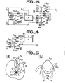
- FIG. 4 also shows a variant relating to the compensation of two differential measurement chains.
- the output signals s 1 and s 2 of the two measuring chains are introduced to the negative and positive inputs of a differential amplifier 41 provided with a feedback resistance R 46 and two input resistors R 46 as well as d 'a resistor R 46 between its non-inverting input and ground.
- the output of amplifier 41 is introduced into a memory 43 by a line 42, and the output 44 corresponding to the reading of the memory is introduced at the negative input of amplifier 41, also through an input resistor R 46 .
- the signal 5 4 corresponds to the output signals S 2 and S 3 of FIGS. 2 and 3.
- FIG. 5 a represents the angular diagrams corresponding to antennas with multiple diagrams the shapes of which are defined so as to be able to better delimit the interrogation arc and to discriminate the responses coming from a main lobe and those coming from the secondary lobes.
- the diagram RS1 presents a main lobe 53 provided with a maximum 54 which corresponds to the geometric axis of the antenna, and a plurality of secondary lobes 55 of lower amplitude.
- the RS2 diagram is in the general form of a cardioid and has a minimum gain of 52 in the main direction constituting the geometric axis of the antenna.
- the RS2 diagram corresponds to an amplitude greater than that of all the secondary lobes 55.
- Figure 5b illustrates the variation of the interrogation arc which can be obtained by adding a constant to the RS2 diagram: the interrogation arc a 2 located closer to the top of RS1 is thus narrower than the arc d 'interrogation a I , which allows a finer interrogation.
- FIG. 6 illustrates the application of a device according to the invention to the compensation of the measurement chains of an RSLS system.
- the compensation will take place by periodically effecting, outside the normal use time of the receiver, the storage of the amplitude of the response associated with a signal of known amplitude. for each of the receivers.
- the response of the receiver to an input signal of any amplitude will be compared to the stored response in order to take into account only the difference between these two signals.
- FIG. 6 thus represents a device corresponding to a diagram equivalent to FIGS. 2 to 4, where the measurement values present at the output of the two chains sri and s r2 are applied respectively to the positive and negative inputs of a differential amplifier 63 provided with a feedback resistance R62, through input resistors R 62 , and where the values memorized respectively by the memories 61 and 62 present at the output of said measurement chains, are applied respectively to the negative and positive inputs of the amplifier differential 63 through R 62 input resistors.
- the compensated signal S6 present at the output of the amplifier 63 will have a positive sign for the signals corresponding to the main lobes 53 of the RSI diagram.
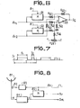
- FIG. 7 illustrates a mode of temporal distribution between the measurement signals and the reference signals in the case of the radar technique.
- the recurrent radar pulses I are separated by time intervals T.
- the measurement takes place during the time interval T 1
- FIG. 8 illustrates the switching carried out at the level of an antenna 81.
- a synchronization pulse brought by a line 86 simultaneously controls an oscillator 83 coupled to the output of the antenna 81 by a coupler 82, and the writing into a memory 85. This will result in a reference pulse applied to the input of the measurement chain 84 as long as. the synchronization pulse is present.
- the stored value S remains permanently present at the - exit from memory M.
- Such a device is particularly advantageous in the case of the technique considered since it constitutes not only compensation for drifts in the reception chain but also compensation for the interference that the radar antenna is capable of detecting. Indeed, interference generally results in the presence at the output of the antenna of a direct voltage which is superimposed on the signal.
- FIG. 9 a which corresponds to the prior art, a pulse present at the output of the antenna and protruding by one quantity h of the continuous level of interference V B will give rise at the output to a pulse of height H whose level is a function of the continuous level of interference V B.
- a pulse present at the output of the antenna and exceeding by an amount h ′ of the reference level VR and by an amount h of the continuous level of interference V B will give rise at the output to a pulse of height H ′ whose height is a function of V R as long as V R remains greater than V B.
- the memorized value V M corresponding to the output of one or the other measurement chain gradually drifts. It is then possible to identify the presence of more or less intense interference by fixing one or more drift thresholds, either in level or in slope, for the memorized value V M. To do this, at least one stored signal V M is introduced into a circuit comprising at least one threshold. Such a check also makes it possible to check the correct operating condition of the measuring chain.
- FIG. 10 illustrates a variant of the invention where a measurement chain 101 is of such quality that it does not have any drift.
- This reference chain operates with at least one other measurement chain 102 which, of quality and lower cost, has drifts which it is necessary to compensate for.
- the values S 1r and S 2r corresponding to an identical reference signal V r applied to the two chains are introduced into a memory 103 which stores their difference (S 2r - S 1r ).
- the output of the memory 103 and of the measurement chain 102 are introduced into a differential amplifier 104 so as to produce at its output a signal S 2m - (S 2r -S 1r ).
- the measurement chains such as 102 are then continuously readjusted relative to the reference chain 101.
Landscapes
- Engineering & Computer Science (AREA)
- Radar, Positioning & Navigation (AREA)
- Remote Sensing (AREA)
- Computer Networks & Wireless Communication (AREA)
- Physics & Mathematics (AREA)
- General Physics & Mathematics (AREA)
- Power Engineering (AREA)
- Radar Systems Or Details Thereof (AREA)
Applications Claiming Priority (2)
| Application Number | Priority Date | Filing Date | Title |
|---|---|---|---|
| FR8105857 | 1981-03-24 | ||
| FR8105857A FR2502866B1 (fr) | 1981-03-24 | 1981-03-24 | Dispositif de compensation des derives d'au moins une chaine de mesure et son application |
Publications (2)
| Publication Number | Publication Date |
|---|---|
| EP0061403A1 true EP0061403A1 (de) | 1982-09-29 |
| EP0061403B1 EP0061403B1 (de) | 1985-02-20 |
Family
ID=9256577
Family Applications (1)
| Application Number | Title | Priority Date | Filing Date |
|---|---|---|---|
| EP19820400507 Expired EP0061403B1 (de) | 1981-03-24 | 1982-03-19 | Gerät zur Driftkompensation für mindestens einen einzigen Messkanal sowie seine Anwendung |
Country Status (3)
| Country | Link |
|---|---|
| EP (1) | EP0061403B1 (de) |
| DE (1) | DE3262371D1 (de) |
| FR (1) | FR2502866B1 (de) |
Cited By (1)
| Publication number | Priority date | Publication date | Assignee | Title |
|---|---|---|---|---|
| EP0374987A1 (de) * | 1988-11-21 | 1990-06-27 | Hollandse Signaalapparaten B.V. | Radargerät und Einheit zur Unterdrückung von Nebenkeulen, angewendet in einem solchen Radargerät |
Citations (4)
| Publication number | Priority date | Publication date | Assignee | Title |
|---|---|---|---|---|
| FR2289018A1 (fr) * | 1974-10-21 | 1976-05-21 | Stanford Research Inst | Procede et dispositif de compensation des variations des caracteristiques de canaux de traitement d'informations |
| US4010469A (en) * | 1951-06-20 | 1977-03-01 | The Rand Corporation | Interference suppression |
| FR2357905A1 (fr) * | 1976-07-07 | 1978-02-03 | Heliowatt Werke | Procede de compensation des erreurs, en particulier pour appareils de mesure transformant les grandeurs analogiques en valeurs numeriques |
| US4078156A (en) * | 1977-01-03 | 1978-03-07 | Avco Corporation | Drift cancellation circuit for multiplexer amplifier |
-
1981
- 1981-03-24 FR FR8105857A patent/FR2502866B1/fr not_active Expired
-
1982
- 1982-03-19 DE DE8282400507T patent/DE3262371D1/de not_active Expired
- 1982-03-19 EP EP19820400507 patent/EP0061403B1/de not_active Expired
Patent Citations (4)
| Publication number | Priority date | Publication date | Assignee | Title |
|---|---|---|---|---|
| US4010469A (en) * | 1951-06-20 | 1977-03-01 | The Rand Corporation | Interference suppression |
| FR2289018A1 (fr) * | 1974-10-21 | 1976-05-21 | Stanford Research Inst | Procede et dispositif de compensation des variations des caracteristiques de canaux de traitement d'informations |
| FR2357905A1 (fr) * | 1976-07-07 | 1978-02-03 | Heliowatt Werke | Procede de compensation des erreurs, en particulier pour appareils de mesure transformant les grandeurs analogiques en valeurs numeriques |
| US4078156A (en) * | 1977-01-03 | 1978-03-07 | Avco Corporation | Drift cancellation circuit for multiplexer amplifier |
Non-Patent Citations (1)
| Title |
|---|
| TOUTE L'ELECTRONIQUE, no. 459, decembre 1980, PARIS (FR) G. MOURIER: "Amplification à très faible dérive: "chopper" ou bipolaires hautes performances" pages 61-65 * |
Cited By (1)
| Publication number | Priority date | Publication date | Assignee | Title |
|---|---|---|---|---|
| EP0374987A1 (de) * | 1988-11-21 | 1990-06-27 | Hollandse Signaalapparaten B.V. | Radargerät und Einheit zur Unterdrückung von Nebenkeulen, angewendet in einem solchen Radargerät |
Also Published As
| Publication number | Publication date |
|---|---|
| EP0061403B1 (de) | 1985-02-20 |
| FR2502866B1 (fr) | 1986-07-18 |
| FR2502866A1 (fr) | 1982-10-01 |
| DE3262371D1 (en) | 1985-03-28 |
Similar Documents
| Publication | Publication Date | Title |
|---|---|---|
| EP0052024A1 (de) | Optoelektronische Anordnung für die videofrequente Bildanalyse durch Abtastung | |
| FR2589649A1 (fr) | Dispositif destine a augmenter la puissance de sortie d'un appareil radioelectrique alimente a basse tension, par exemple du type autoradio | |
| EP0456546A1 (de) | Empfänger für bekannte Frequenz mit unbekannter Frequenzabweichung, insbesondere einer Dopplerverschiebung | |
| EP0436222B1 (de) | Schaltung zur digitalen Messung eines elektrischen Signals | |
| FR2717907A1 (fr) | Radar de poursuite. | |
| EP0573321B1 (de) | Verfahren und Einrichtung zur automatischen Kompensation der Nichtlinearität der Modulationsgeraden für Radar mit Frequenzmodulation | |
| EP0715184A1 (de) | Verfahren und Vorrichtung zur Bestimmung der Geschwindigkeit eines bewegbaren Körpers mittels eines Radars oder Sonars mit Impulskompression | |
| CA1226654A (fr) | Dispositif de discrimination d'echos radar | |
| EP0022410B1 (de) | Sondiergerät zum Bestimmen und Messen relativer Phänomene in der Umgebung des Erdballs | |
| EP0061403B1 (de) | Gerät zur Driftkompensation für mindestens einen einzigen Messkanal sowie seine Anwendung | |
| EP0637147B1 (de) | Abstimmungsvorrichtung eines optischen abstimmbaren Filters insbesondere zur Anwendung beim Empfang in einem optischen Übertragungssystem | |
| EP0727675B1 (de) | Abfragegerät für ein Identifizierungssystem mittels Radiodetektion | |
| EP0211714B1 (de) | Einrichtung zur Dynamikerhöhung einer Verstärkerschaltung, insbesondere eines MLS-Bordempfängers | |
| EP3538916B1 (de) | Verfahren zum testen der elektromagnetischen verträglichkeit eines radardetektors mit mindestens einem impulssignalsender an bord | |
| EP0053963B1 (de) | Quantifizierungsanordnung für Pulssignale für Sekundärradar | |
| FR2550347A1 (fr) | Perfectionnements aux radars doppler a impulsions | |
| EP0055636B1 (de) | Abweichungsempfänger für Sekundärradar | |
| EP0796421B1 (de) | Filtervorrichtung, insbesondere für die kraftstoffanzeige in automobilen | |
| EP0778471B1 (de) | Verfahren und Vorrichtung zur Radardetektion | |
| EP0335753A1 (de) | Radar zum Korrigieren des Artillerieabfeuerns | |
| FR2621399A1 (fr) | Reseau de reception avec annulation d'interferences | |
| EP0720028A1 (de) | Multifunktionelles, unauffälliges Entfernungsmessgerät | |
| EP3538919B1 (de) | Verfahren zum testen der elektromagnetischen verträglichkeit eines radardetektors mit mindestens einem impulssignalgeber an bord | |
| EP3538917B1 (de) | Verfahren zum testen der elektromagnetischen verträglichkeit eines radardetektors mit mindestens einem impulssignalgeber an bord | |
| FR2684767A1 (fr) | Radar a ouverture synthetique. |
Legal Events
| Date | Code | Title | Description |
|---|---|---|---|
| PUAI | Public reference made under article 153(3) epc to a published international application that has entered the european phase |
Free format text: ORIGINAL CODE: 0009012 |
|
| AK | Designated contracting states |
Designated state(s): DE GB IT NL |
|
| 17P | Request for examination filed |
Effective date: 19821011 |
|
| ITF | It: translation for a ep patent filed | ||
| GRAA | (expected) grant |
Free format text: ORIGINAL CODE: 0009210 |
|
| AK | Designated contracting states |
Designated state(s): DE GB IT NL |
|
| REF | Corresponds to: |
Ref document number: 3262371 Country of ref document: DE Date of ref document: 19850328 |
|
| PLBE | No opposition filed within time limit |
Free format text: ORIGINAL CODE: 0009261 |
|
| STAA | Information on the status of an ep patent application or granted ep patent |
Free format text: STATUS: NO OPPOSITION FILED WITHIN TIME LIMIT |
|
| 26N | No opposition filed | ||
| PGFP | Annual fee paid to national office [announced via postgrant information from national office to epo] |
Ref country code: GB Payment date: 19930225 Year of fee payment: 12 Ref country code: DE Payment date: 19930225 Year of fee payment: 12 |
|
| ITTA | It: last paid annual fee | ||
| PGFP | Annual fee paid to national office [announced via postgrant information from national office to epo] |
Ref country code: NL Payment date: 19930331 Year of fee payment: 12 |
|
| PG25 | Lapsed in a contracting state [announced via postgrant information from national office to epo] |
Ref country code: GB Effective date: 19940319 |
|
| PG25 | Lapsed in a contracting state [announced via postgrant information from national office to epo] |
Ref country code: NL Effective date: 19941001 |
|
| GBPC | Gb: european patent ceased through non-payment of renewal fee |
Effective date: 19940319 |
|
| NLV4 | Nl: lapsed or anulled due to non-payment of the annual fee | ||
| PG25 | Lapsed in a contracting state [announced via postgrant information from national office to epo] |
Ref country code: DE Effective date: 19941201 |