EP0061615B1 - Ensemble de test électrique comprenant des éléments contacteurs à rotation - Google Patents
Ensemble de test électrique comprenant des éléments contacteurs à rotation Download PDFInfo
- Publication number
- EP0061615B1 EP0061615B1 EP82101854A EP82101854A EP0061615B1 EP 0061615 B1 EP0061615 B1 EP 0061615B1 EP 82101854 A EP82101854 A EP 82101854A EP 82101854 A EP82101854 A EP 82101854A EP 0061615 B1 EP0061615 B1 EP 0061615B1
- Authority
- EP
- European Patent Office
- Prior art keywords
- probe
- elements
- probe assembly
- assembly
- rotating element
- Prior art date
- Legal status (The legal status is an assumption and is not a legal conclusion. Google has not performed a legal analysis and makes no representation as to the accuracy of the status listed.)
- Expired
Links
- 239000000523 sample Substances 0.000 title claims description 126
- 239000000463 material Substances 0.000 claims description 5
- 229910045601 alloy Inorganic materials 0.000 claims description 2
- 239000000956 alloy Substances 0.000 claims description 2
- 229910052737 gold Inorganic materials 0.000 claims description 2
- 229910052751 metal Inorganic materials 0.000 claims description 2
- 239000002184 metal Substances 0.000 claims description 2
- 229910052697 platinum Inorganic materials 0.000 claims description 2
- 229910052709 silver Inorganic materials 0.000 claims description 2
- WFKWXMTUELFFGS-UHFFFAOYSA-N tungsten Chemical compound [W] WFKWXMTUELFFGS-UHFFFAOYSA-N 0.000 claims description 2
- 229910052721 tungsten Inorganic materials 0.000 claims description 2
- 239000010937 tungsten Substances 0.000 claims description 2
- 239000000758 substrate Substances 0.000 description 7
- 229910052782 aluminium Inorganic materials 0.000 description 6
- XAGFODPZIPBFFR-UHFFFAOYSA-N aluminium Chemical compound [Al] XAGFODPZIPBFFR-UHFFFAOYSA-N 0.000 description 6
- 239000011159 matrix material Substances 0.000 description 6
- 230000000712 assembly Effects 0.000 description 5
- 238000000429 assembly Methods 0.000 description 5
- 238000000576 coating method Methods 0.000 description 4
- 238000007790 scraping Methods 0.000 description 4
- 239000004065 semiconductor Substances 0.000 description 4
- 239000011248 coating agent Substances 0.000 description 2
- 230000002068 genetic effect Effects 0.000 description 2
- BASFCYQUMIYNBI-UHFFFAOYSA-N platinum Chemical compound [Pt] BASFCYQUMIYNBI-UHFFFAOYSA-N 0.000 description 2
- 229910000679 solder Inorganic materials 0.000 description 2
- BQCADISMDOOEFD-UHFFFAOYSA-N Silver Chemical compound [Ag] BQCADISMDOOEFD-UHFFFAOYSA-N 0.000 description 1
- 238000003491 array Methods 0.000 description 1
- 238000005452 bending Methods 0.000 description 1
- 239000000919 ceramic Substances 0.000 description 1
- PCHJSUWPFVWCPO-UHFFFAOYSA-N gold Chemical compound [Au] PCHJSUWPFVWCPO-UHFFFAOYSA-N 0.000 description 1
- 239000010931 gold Substances 0.000 description 1
- 238000005272 metallurgy Methods 0.000 description 1
- 238000000034 method Methods 0.000 description 1
- 229910052759 nickel Inorganic materials 0.000 description 1
- TWNQGVIAIRXVLR-UHFFFAOYSA-N oxo(oxoalumanyloxy)alumane Chemical compound O=[Al]O[Al]=O TWNQGVIAIRXVLR-UHFFFAOYSA-N 0.000 description 1
- 230000000149 penetrating effect Effects 0.000 description 1
- 230000002093 peripheral effect Effects 0.000 description 1
- 239000011347 resin Substances 0.000 description 1
- 229920005989 resin Polymers 0.000 description 1
- 239000004332 silver Substances 0.000 description 1
Images

Classifications
-
- G—PHYSICS
- G01—MEASURING; TESTING
- G01R—MEASURING ELECTRIC VARIABLES; MEASURING MAGNETIC VARIABLES
- G01R1/00—Details of instruments or arrangements of the types included in groups G01R5/00 - G01R13/00 and G01R31/00
- G01R1/02—General constructional details
- G01R1/06—Measuring leads; Measuring probes
- G01R1/067—Measuring probes
- G01R1/073—Multiple probes
-
- G—PHYSICS
- G01—MEASURING; TESTING
- G01R—MEASURING ELECTRIC VARIABLES; MEASURING MAGNETIC VARIABLES
- G01R1/00—Details of instruments or arrangements of the types included in groups G01R5/00 - G01R13/00 and G01R31/00
- G01R1/02—General constructional details
- G01R1/06—Measuring leads; Measuring probes
- G01R1/067—Measuring probes
- G01R1/073—Multiple probes
- G01R1/07307—Multiple probes with individual probe elements, e.g. needles, cantilever beams or bump contacts, fixed in relation to each other, e.g. bed of nails fixture or probe card
- G01R1/07314—Multiple probes with individual probe elements, e.g. needles, cantilever beams or bump contacts, fixed in relation to each other, e.g. bed of nails fixture or probe card the body of the probe being perpendicular to test object, e.g. bed of nails or probe with bump contacts on a rigid support
-
- G—PHYSICS
- G01—MEASURING; TESTING
- G01R—MEASURING ELECTRIC VARIABLES; MEASURING MAGNETIC VARIABLES
- G01R1/00—Details of instruments or arrangements of the types included in groups G01R5/00 - G01R13/00 and G01R31/00
- G01R1/02—General constructional details
- G01R1/06—Measuring leads; Measuring probes
- G01R1/067—Measuring probes
- G01R1/073—Multiple probes
- G01R1/07307—Multiple probes with individual probe elements, e.g. needles, cantilever beams or bump contacts, fixed in relation to each other, e.g. bed of nails fixture or probe card
- G01R1/07357—Multiple probes with individual probe elements, e.g. needles, cantilever beams or bump contacts, fixed in relation to each other, e.g. bed of nails fixture or probe card with flexible bodies, e.g. buckling beams
-
- H—ELECTRICITY
- H01—ELECTRIC ELEMENTS
- H01R—ELECTRICALLY-CONDUCTIVE CONNECTIONS; STRUCTURAL ASSOCIATIONS OF A PLURALITY OF MUTUALLY-INSULATED ELECTRICAL CONNECTING ELEMENTS; COUPLING DEVICES; CURRENT COLLECTORS
- H01R12/00—Structural associations of a plurality of mutually-insulated electrical connecting elements, specially adapted for printed circuits, e.g. printed circuit boards [PCB], flat or ribbon cables, or like generally planar structures, e.g. terminal strips, terminal blocks; Coupling devices specially adapted for printed circuits, flat or ribbon cables, or like generally planar structures; Terminals specially adapted for contact with, or insertion into, printed circuits, flat or ribbon cables, or like generally planar structures
- H01R12/70—Coupling devices
- H01R12/71—Coupling devices for rigid printing circuits or like structures
- H01R12/712—Coupling devices for rigid printing circuits or like structures co-operating with the surface of the printed circuit or with a coupling device exclusively provided on the surface of the printed circuit
- H01R12/714—Coupling devices for rigid printing circuits or like structures co-operating with the surface of the printed circuit or with a coupling device exclusively provided on the surface of the printed circuit with contacts abutting directly the printed circuit; Button contacts therefore provided on the printed circuit
Definitions
- the invention relates to probe assemblies for making electrical contact to closely spaced pads on electrical devices and substrates, the probe assemblies being capable of positively establishing electrical contact to a matrix of pads by using a unique scraping action capable of penetrating surface dielectric layers on the pads.
- a genetic layer of AI 2 0 3 is inherently formed on an aluminum surface upon exposure to air forming a tough coating that makes the establishment of electrical contact very difficult, particularly with very small contact pads necessary in highly miniaturized devices with closely spaced matrix of pads. Any wiping or scraping action of the buckling beam type probe is not sufficient to dependably establish electrical contact.
- This invention overcomes the above problems by using a rotating probe element action that dependably and consistently scrapes away surface A1 2 0 3 from aluminum pads, and other similar oxides and coatings to thereby establish good electrical contact.
- the rotatable elongated probe elements are capable of breaking through surface oxide, thin coatings, and the like on contact pads of the device or substrate to be tested, and thereby consistently and dependably establish electrical contact to the pad to permit electrical testing of the device or substrate.
- the probe of the invention is particularly adapted for the testing of very small, closely spaced pad configurations, particularly . pad matrixes formed of aluminum.
- the probe assembly is capable of breaking through the inherent genetic aluminum oxide layer on aluminum pads.
- the electrical probe assembly of the invention has a plurality of elongated probe elements formed of conductive flexible material, each having a length many times its diameter.
- Spaced upper and lower flat support elements having apertures receive the ends of the probe elements and maintain the probe elements in a generally parallel arrangement with at least the lower ends supported in a configuration corresponding to the pad configuration to be contacted and protruding beyond the lower support element.
- a means is provided to simultaneously rotate the probe element to provide a cutting or scraping action.
- the means to rotate the probe element can be either an actuating element such as a solenoid or air cylinder, or alternatively, an arrangement utilizing the buckling of the probe element when the probe element is brought into contact with the pads and forced downwardly.
- This probe assembly breaks through the surface oxide or other coating by rotation of the probe element which has a sharp cutting edge on the tip.
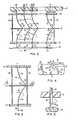
- Fig. 1 of the drawings illustrates a preferred specific embodiment of the probe assembly 10 in combination with a space transformer 12 and a printed circuit board 14.
- Elongated probe elements 16 are mounted in a generally upright or vertical arrangement in probe assembly 10 so that the lower ends 18 protrude to contact the pad configuration on the device or substrate to be tested.
- Probe elements 16 are supported in-a suitable configuration, as for example a grid with the lower protruding ends 18 arranged to correspond to the pad matrix on the substrate to be tested.
- the upper ends of probe element 16 make electrical contact to a pad configuration 20 on the lower surface of space transformer 12.
- the space transformer is a suitable element with a fan out pattern that spreads out the contacts 20 to pads 22 on the top surface of space transformer 12.
- the fan out configuration can be of any suitable type in one or more layers on the top or bottom surface of the transformer or sandwiched in the center.
- Space transformer 12 can be made of any suitable material as for example resin or ceramic.
- Printed circuit board 14 has a set of contact pads 30 on the lower side thereof in a configuration that matches the pads 22 on the space transformer. Fan out metallurgy 32 further expands the spacing to terminals 34. Terminals 34 are connected to a suitable tester.
- each probe element 16 in probe assembly 10 is electrically connected to a corresponding terminal 34 in printed circuit board through space transformer 12.
- the space transformer and printed circuit board assembly is typical of an arrangement for making electrical contact to the probe element 16.
- Other suitable systems for connecting the probe assembly 10 to a tester can be substituted for the one illustrated.
- Probe elements 16 are pre-bent as illustrated in Fig. 1.
- the upper ends of probe elements 16 are rotatably supported in a flat upper support element 36 mounted on base 38, and the lower ends are supported in a lower flat support element 40, also supported on base 38.
- a flat probe rotating element 42 receives the central portions of pre-bent probe elements 16 in apertures 44 and is provided with a suitable camming arrangement that constrains movement of the probe rotating element 42 to an arcuate movement. This arcuate movement rotates the probe element 16 approximately 85° or less.
- Probe rotating element 42 has arcuate cam surfaces, not shown, in which are seated cam follower pins 46.
- the upper ends of probe elements 16 must make electrical contact to the transformer element 12. This contacting arrangement can be achieved in a various number of ways.
- the electrical can be established by providing a ball surface 80 preferably plated with an inert metal such as gold, silver, platinum or alloys thereof.
- the end of probe 16 can be provided with a bevelled surface 82 or a wire 84 can be bonded to the end portion protruding above element 36.
- Yet another technique would be to form a convoluted configuration 86 which can be suitably connected to the connecting circuitry.
- each probe 16 is preferably pre-bent and shaped with a central portion 48 received in aperture 50 of element 42, an upper arcuate-shaped portion 52 joined to central portion 48 and with the upper end making electrical contact with a pad or pin in space transformer board 12, and a lower arcuate portion 54 joined to central portion 48 and with the lower end provided with a sharp point 56 that makes electrical contact with pads 58 on substrate 60.
- the lower end 54 of probe element 16 is provided with a bevelled surface 56 resulting in a sharp cutting edge.
- the bevelled surface of the probe will define any suitable angle relative to the surface of pad 58, preferably making an angle in the range of 15° to 60°, most preferably in the range of 30° to 45°.
- probe rotating element 42 is located between flat support elements 36 and 40. Probe elements 16 extend through probe rotating element 42 through apertures 50 having the same general configuration as the apertures in elements 36 and 40. Probe rotating element 42 has a camming arrangement that constrains the element to move in an arcuate path to thereby rotate probe element 16 about an arc somewhat less than 90°.
- the camming arrangement is shown in Fig. 4 wherein camming surface 62 consists of a slot receiving cam follower pin 46. The resulting arcuate movement of probe rotating element 46 is indicated by arrow 54.
- Probe rotating element 42 can be actuated by any suitable means as for example a solenoid or an air valve connected to a suitable linkage.
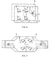
- Fig. 7 illustrates the initial and the final position of the probe rotating element before and after it has been actuated. The solid line figure indicates the initial position and the dotted line figure indicates the subsequent position including the probe element 16.
- the probe rotating element is actuated by the flexing or bending movement of the probe 16 following contact with the pads 58 on a substrate 60.
- Each of the probe elements 16 has a length that is many times its diameter.
- a preferred probe element for use in the practice of the invention has a length in the range of 7,62 to 22,86 mm (300 to 900 mils), and a diameter in the range of 0.05 to 0.16 mm (2 to 6 mils); its central portion 48 is displaced from the longitudinal axis extending through its ends by a distance in the range of 1.27 to 3.81 mm (50 to 150 mils).
- Probe elements 16 are formed of a spring-like material, preferably tungsten, Be Ni and Be Cu.
- Fig. 6 illustrates the relative position of the probe rotating element 42 before and after it has been actuated by flexing of the probe element 16.
- the solid line figure is the initial position and the dotted line figure is the subsequent position after the probes have been rotated.
- Fig. 4 illustrates the relative position of the camming surfaces and the probe element necessary for movement of the probe rotating element.
- the initial position of the probe element indicated by 16 is offset from a longitudinal line 63 parallel to an axis connecting cam follower pins 46 as indicated by arc 70.
- the flexed pin 16 exerts a force 72 which can be broken down into a longitudinal force 74 and a lateral force 76.
- the camming assembly prevents any movement in the direction of arrow 74 but allows movement in the general direction of arrow 64. Further flexing of the probe element causes the arcuate movement of probe rotating element 42 along the path dictated by the camming assembly, thereby resulting in a partial rotation of probe element 16.
- the ends of probe elements 16 can be shaped in any suitable manner to suit the particular application. The ends can be flat when the probe is used to contact solder pads since rotation of a flat probe element is sufficient to penetrate any oxide over the relatively soft solder material.
Landscapes
- Physics & Mathematics (AREA)
- General Physics & Mathematics (AREA)
- Measuring Leads Or Probes (AREA)
- Testing Or Measuring Of Semiconductors Or The Like (AREA)
- Testing Of Individual Semiconductor Devices (AREA)
Claims (12)
Applications Claiming Priority (2)
| Application Number | Priority Date | Filing Date | Title |
|---|---|---|---|
| US245818 | 1981-03-20 | ||
| US06/245,818 US4423376A (en) | 1981-03-20 | 1981-03-20 | Contact probe assembly having rotatable contacting probe elements |
Publications (3)
| Publication Number | Publication Date |
|---|---|
| EP0061615A2 EP0061615A2 (fr) | 1982-10-06 |
| EP0061615A3 EP0061615A3 (en) | 1983-09-14 |
| EP0061615B1 true EP0061615B1 (fr) | 1985-12-27 |
Family
ID=22928204
Family Applications (1)
| Application Number | Title | Priority Date | Filing Date |
|---|---|---|---|
| EP82101854A Expired EP0061615B1 (fr) | 1981-03-20 | 1982-03-09 | Ensemble de test électrique comprenant des éléments contacteurs à rotation |
Country Status (4)
| Country | Link |
|---|---|
| US (1) | US4423376A (fr) |
| EP (1) | EP0061615B1 (fr) |
| JP (1) | JPS5952541B2 (fr) |
| DE (1) | DE3268074D1 (fr) |
Cited By (1)
| Publication number | Priority date | Publication date | Assignee | Title |
|---|---|---|---|---|
| US7714598B2 (en) | 1993-11-16 | 2010-05-11 | Formfactor, Inc. | Contact carriers (tiles) for populating larger substrates with spring contacts |
Families Citing this family (91)
| Publication number | Priority date | Publication date | Assignee | Title |
|---|---|---|---|---|
| US4506215A (en) * | 1981-06-30 | 1985-03-19 | International Business Machines Corporation | Modular test probe |
| JPS587836A (ja) * | 1981-06-30 | 1983-01-17 | インタ−ナショナル ビジネス マシ−ンズ コ−ポレ−ション | プロ−ブ・アツセンブリ− |
| JPS5929151B2 (ja) * | 1981-08-03 | 1984-07-18 | 日本電子材料株式会社 | 半導体ウエハ−試験装置 |
| US4540229A (en) * | 1982-04-12 | 1985-09-10 | At&T Bell Laboratories | Electrical interconnection apparatus |
| US4788496A (en) * | 1982-11-05 | 1988-11-29 | Martin Maelzer | Adapter for a printed circuit board testing device |
| JPS60142530A (ja) * | 1983-12-28 | 1985-07-27 | Yokowo Mfg Co Ltd | 回路基板等の検査装置 |
| DE3539720A1 (de) * | 1985-11-08 | 1987-05-14 | Martin Maelzer | Adapter fuer ein leiterplattenpruefgeraet |
| JPS62257066A (ja) * | 1986-05-01 | 1987-11-09 | Yamaichi Seiko:Kk | 回転式フレキシブルコンタクトプロ−ブ |
| DE3734647A1 (de) * | 1986-10-14 | 1988-04-21 | Feinmetall Gmbh | Nadelkarte |
| DE3736689A1 (de) * | 1986-11-18 | 1988-05-26 | Luther Erich | Adapter fuer ein leiterplattenpruefgeraet |
| JPS6439742A (en) * | 1987-08-06 | 1989-02-10 | Tokyo Electron Ltd | Probe card |
| US4963822A (en) * | 1988-06-01 | 1990-10-16 | Manfred Prokopp | Method of testing circuit boards and the like |
| DE4035978A1 (de) * | 1990-02-16 | 1991-08-22 | Luther Erich | Verfahren und vorrichtung zum laden eines adapters fuer ein leiterplattenpruefgeraet |
| US5123848A (en) * | 1990-07-20 | 1992-06-23 | Cray Research, Inc. | Computer signal interconnect apparatus |
| US5175496A (en) * | 1990-08-31 | 1992-12-29 | Cray Research, Inc. | Dual contact beam assembly for an IC test fixture |
| US5113133A (en) * | 1990-12-20 | 1992-05-12 | Integri-Test Corporation | Circuit board test probe |
| JPH0675415B2 (ja) * | 1991-03-15 | 1994-09-21 | 山一電機株式会社 | リードレス形icパッケージ用接続器 |
| JPH05215773A (ja) * | 1992-02-04 | 1993-08-24 | Nhk Spring Co Ltd | 多点測定用導電性接触子ユニット |
| US5415559A (en) * | 1992-05-18 | 1995-05-16 | Japan Aviation Electronics Industry, Ltd. | Electrical connector having a plurality of contact pin springs |
| US20050062492A1 (en) * | 2001-08-03 | 2005-03-24 | Beaman Brian Samuel | High density integrated circuit apparatus, test probe and methods of use thereof |
| US5367254A (en) * | 1993-02-01 | 1994-11-22 | International Business Machines Corporation | Test probe assembly using buckling wire probes within tubes having opposed overlapping slots |
| US20030048108A1 (en) * | 1993-04-30 | 2003-03-13 | Beaman Brian Samuel | Structural design and processes to control probe position accuracy in a wafer test probe assembly |
| US20020053734A1 (en) | 1993-11-16 | 2002-05-09 | Formfactor, Inc. | Probe card assembly and kit, and methods of making same |
| US7073254B2 (en) | 1993-11-16 | 2006-07-11 | Formfactor, Inc. | Method for mounting a plurality of spring contact elements |
| US6246247B1 (en) * | 1994-11-15 | 2001-06-12 | Formfactor, Inc. | Probe card assembly and kit, and methods of using same |
| AU4160096A (en) * | 1994-11-15 | 1996-06-06 | Formfactor, Inc. | Probe card assembly and kit, and methods of using same |
| EP1610375A3 (fr) * | 1995-05-26 | 2008-11-05 | FormFactor, Inc. | Support de contact pour équiper des substrats avec des contacts à lames |
| US20100065963A1 (en) | 1995-05-26 | 2010-03-18 | Formfactor, Inc. | Method of wirebonding that utilizes a gas flow within a capillary from which a wire is played out |
| US8033838B2 (en) | 1996-02-21 | 2011-10-11 | Formfactor, Inc. | Microelectronic contact structure |
| FR2748813B1 (fr) * | 1996-05-14 | 1998-07-10 | Chasserieau Claude | Dispositif de test, notamment d'un composant electronique a multicontacts |
| US5764072A (en) * | 1996-12-20 | 1998-06-09 | Probe Technology | Dual contact probe assembly for testing integrated circuits |
| US6690185B1 (en) | 1997-01-15 | 2004-02-10 | Formfactor, Inc. | Large contactor with multiple, aligned contactor units |
| ATE261129T1 (de) * | 1997-11-05 | 2004-03-15 | Feinmetall Gmbh | Prüfkopf für mikrostrukturen mit schnittstelle |
| EP0915344B1 (fr) * | 1997-11-05 | 2004-02-25 | Feinmetall GmbH | Tête de sonde pour microstructures avec interface |
| FR2772921B1 (fr) * | 1997-12-24 | 2000-01-28 | Sgs Thomson Microelectronics | Carte a pointes pour le test de composants semi-conducteurs |
| US6799976B1 (en) | 1999-07-28 | 2004-10-05 | Nanonexus, Inc. | Construction structures and manufacturing processes for integrated circuit wafer probe card assemblies |
| US7247035B2 (en) | 2000-06-20 | 2007-07-24 | Nanonexus, Inc. | Enhanced stress metal spring contactor |
| US7349223B2 (en) | 2000-05-23 | 2008-03-25 | Nanonexus, Inc. | Enhanced compliant probe card systems having improved planarity |
| US7382142B2 (en) | 2000-05-23 | 2008-06-03 | Nanonexus, Inc. | High density interconnect system having rapid fabrication cycle |
| US6812718B1 (en) | 1999-05-27 | 2004-11-02 | Nanonexus, Inc. | Massively parallel interface for electronic circuits |
| US7215131B1 (en) | 1999-06-07 | 2007-05-08 | Formfactor, Inc. | Segmented contactor |
| US6255832B1 (en) * | 1999-12-03 | 2001-07-03 | International Business Machines Corporation | Flexible wafer level probe |
| US7262611B2 (en) | 2000-03-17 | 2007-08-28 | Formfactor, Inc. | Apparatuses and methods for planarizing a semiconductor contactor |
| US6529021B1 (en) | 2000-04-25 | 2003-03-04 | International Business Machines Corporation | Self-scrub buckling beam probe |
| US7579848B2 (en) | 2000-05-23 | 2009-08-25 | Nanonexus, Inc. | High density interconnect system for IC packages and interconnect assemblies |
| US7952373B2 (en) | 2000-05-23 | 2011-05-31 | Verigy (Singapore) Pte. Ltd. | Construction structures and manufacturing processes for integrated circuit wafer probe card assemblies |
| US6650133B1 (en) * | 2000-10-25 | 2003-11-18 | Intel Corporation | Method and apparatus for buckling beam testing |
| DE10053745B4 (de) * | 2000-10-30 | 2004-07-15 | Heigl, Helmuth, Dr.-Ing. | Vorrichtung und Verfahren zur Kontaktierung eines oder mehrerer Anschlüsse an einem elektronischen Bauteil |
| DE10057456A1 (de) * | 2000-11-20 | 2002-05-23 | Test Plus Electronic Gmbh | Anordnung zum Verbinden von Testnadeln eines Testadapters mit einer Prüfeinrichtung |
| JP2002231399A (ja) * | 2001-02-02 | 2002-08-16 | Fujitsu Ltd | 半導体装置試験用コンタクタ及びその製造方法 |
| US6729019B2 (en) | 2001-07-11 | 2004-05-04 | Formfactor, Inc. | Method of manufacturing a probe card |
| WO2003087853A1 (fr) * | 2002-04-16 | 2003-10-23 | Nhk Spring Co., Ltd | Support destine a un contact conducteur |
| US7059046B2 (en) * | 2002-06-24 | 2006-06-13 | Delaware Capital Formation, Inc. | Method for producing a captive wired test fixture and fixture therefor |
| JP2004132971A (ja) * | 2002-09-17 | 2004-04-30 | Iwasaki Correspond Industry Co Ltd | プローブカード |
| AU2003211215A1 (en) * | 2003-02-17 | 2004-09-06 | Kabushiki Kaisha Nihon Micronics | Electrical connection device |
| US7176702B2 (en) * | 2004-04-07 | 2007-02-13 | Micron Technology, Inc. | Contact system for wafer level testing |
| US7733101B2 (en) * | 2004-05-21 | 2010-06-08 | Microprobe, Inc. | Knee probe having increased scrub motion |
| US7659739B2 (en) | 2006-09-14 | 2010-02-09 | Micro Porbe, Inc. | Knee probe having reduced thickness section for control of scrub motion |
| USRE43503E1 (en) | 2006-06-29 | 2012-07-10 | Microprobe, Inc. | Probe skates for electrical testing of convex pad topologies |
| US8988091B2 (en) | 2004-05-21 | 2015-03-24 | Microprobe, Inc. | Multiple contact probes |
| US9476911B2 (en) | 2004-05-21 | 2016-10-25 | Microprobe, Inc. | Probes with high current carrying capability and laser machining methods |
| US7759949B2 (en) | 2004-05-21 | 2010-07-20 | Microprobe, Inc. | Probes with self-cleaning blunt skates for contacting conductive pads |
| US9097740B2 (en) | 2004-05-21 | 2015-08-04 | Formfactor, Inc. | Layered probes with core |
| DE102004027886A1 (de) * | 2004-05-28 | 2005-12-22 | Feinmetall Gmbh | Prüfeinrichtung zur elektrischen Prüfung eines Prüflings sowie Verfahren zur Herstellung einer Prüfeinrichtung |
| US20060066328A1 (en) * | 2004-09-30 | 2006-03-30 | Probelogic, Inc. | Buckling beam probe test assembly |
| US7649367B2 (en) | 2005-12-07 | 2010-01-19 | Microprobe, Inc. | Low profile probe having improved mechanical scrub and reduced contact inductance |
| DE102006005522A1 (de) * | 2006-02-07 | 2007-08-16 | Feinmetall Gmbh | Elektrische Kontaktiervorrichtung sowie elektrisches Kontaktierverfahren |
| US7312617B2 (en) | 2006-03-20 | 2007-12-25 | Microprobe, Inc. | Space transformers employing wire bonds for interconnections with fine pitch contacts |
| US8907689B2 (en) | 2006-10-11 | 2014-12-09 | Microprobe, Inc. | Probe retention arrangement |
| US7786740B2 (en) | 2006-10-11 | 2010-08-31 | Astria Semiconductor Holdings, Inc. | Probe cards employing probes having retaining portions for potting in a potting region |
| US7557303B2 (en) * | 2006-12-18 | 2009-07-07 | Lsi Corporation | Electronic component connection support structures including air as a dielectric |
| US7514948B2 (en) | 2007-04-10 | 2009-04-07 | Microprobe, Inc. | Vertical probe array arranged to provide space transformation |
| US8723546B2 (en) | 2007-10-19 | 2014-05-13 | Microprobe, Inc. | Vertical guided layered probe |
| US7671610B2 (en) | 2007-10-19 | 2010-03-02 | Microprobe, Inc. | Vertical guided probe array providing sideways scrub motion |
| KR101061593B1 (ko) * | 2008-04-21 | 2011-09-01 | 윌테크놀러지(주) | 프로브 카드 |
| US8230593B2 (en) | 2008-05-29 | 2012-07-31 | Microprobe, Inc. | Probe bonding method having improved control of bonding material |
| JP5868239B2 (ja) * | 2012-03-27 | 2016-02-24 | 株式会社日本マイクロニクス | プローブ及びプローブカード |
| US8994393B2 (en) | 2012-09-06 | 2015-03-31 | International Business Machines Corporation | High-frequency cobra probe |
| JP2014169928A (ja) * | 2013-03-04 | 2014-09-18 | Fujitsu Semiconductor Ltd | 検査用ソケット |
| KR102165662B1 (ko) * | 2015-03-31 | 2020-10-14 | 가부시키가이샤 엔프라스 | 전기 접촉자 및 전기 부품용 소켓 |
| WO2016158567A1 (fr) * | 2015-03-31 | 2016-10-06 | 株式会社エンプラス | Prise pour composants électriques et son procédé de production |
| JP6559999B2 (ja) * | 2015-03-31 | 2019-08-14 | 株式会社エンプラス | 電気部品用ソケット |
| US10732202B2 (en) | 2016-03-29 | 2020-08-04 | Globalfoundries Inc. | Repairable rigid test probe card assembly |
| JP6855185B2 (ja) * | 2016-07-27 | 2021-04-07 | 株式会社日本マイクロニクス | 電気的接続装置 |
| TWI596346B (zh) * | 2016-08-24 | 2017-08-21 | 中華精測科技股份有限公司 | 垂直式探針卡之探針裝置 |
| JP6892235B2 (ja) * | 2016-10-05 | 2021-06-23 | 株式会社日本マイクロニクス | 電気的接続装置及び電気的接続装置の製造方法 |
| JP2018179721A (ja) * | 2017-04-12 | 2018-11-15 | 株式会社日本マイクロニクス | 電気的接続装置 |
| CN113671353B (zh) * | 2020-11-29 | 2022-05-17 | 法特迪精密科技(苏州)有限公司 | 一种插座结构 |
| US11742295B2 (en) * | 2020-12-28 | 2023-08-29 | Global Unichip Corporation | Interface of integrated circuit die and method for arranging interface thereof |
| WO2025034206A1 (fr) * | 2023-08-07 | 2025-02-13 | Microfabrica Inc. | Sondes à broches souples à multiples segments de ressort et structures de stabilisation de déflexion du ressort de compression |
| CN118068821B (zh) * | 2024-04-22 | 2024-07-02 | 常州泰尔格重工机械有限公司 | 一种水下机器人控制板检测装置及其检测方法 |
Family Cites Families (5)
| Publication number | Priority date | Publication date | Assignee | Title |
|---|---|---|---|---|
| DE1954558A1 (de) * | 1968-12-20 | 1970-07-09 | Rft Messelektronik Dresden Veb | Kontakteinrichtung |
| US3806801A (en) * | 1972-12-26 | 1974-04-23 | Ibm | Probe contactor having buckling beam probes |
| FR2236339A1 (en) * | 1973-07-05 | 1975-01-31 | Demaria Lapierre Et Mollier | Circuit board component mounting machine - guides and cuts off component leads inserted through holes in board |
| BE847127A (fr) * | 1975-10-17 | 1977-01-31 | Appareil de connexion de controle electrique, | |
| US4027935A (en) * | 1976-06-21 | 1977-06-07 | International Business Machines Corporation | Contact for an electrical contactor assembly |
-
1981
- 1981-03-20 US US06/245,818 patent/US4423376A/en not_active Expired - Lifetime
- 1981-12-11 JP JP56198692A patent/JPS5952541B2/ja not_active Expired
-
1982
- 1982-03-09 EP EP82101854A patent/EP0061615B1/fr not_active Expired
- 1982-03-09 DE DE8282101854T patent/DE3268074D1/de not_active Expired
Cited By (1)
| Publication number | Priority date | Publication date | Assignee | Title |
|---|---|---|---|---|
| US7714598B2 (en) | 1993-11-16 | 2010-05-11 | Formfactor, Inc. | Contact carriers (tiles) for populating larger substrates with spring contacts |
Also Published As
| Publication number | Publication date |
|---|---|
| JPS5952541B2 (ja) | 1984-12-20 |
| US4423376A (en) | 1983-12-27 |
| DE3268074D1 (en) | 1986-02-06 |
| JPS57162442A (en) | 1982-10-06 |
| EP0061615A2 (fr) | 1982-10-06 |
| EP0061615A3 (en) | 1983-09-14 |
Similar Documents
| Publication | Publication Date | Title |
|---|---|---|
| EP0061615B1 (fr) | Ensemble de test électrique comprenant des éléments contacteurs à rotation | |
| US5828226A (en) | Probe card assembly for high density integrated circuits | |
| EP0453716B1 (fr) | Connecteur assemblage pour tester des puces | |
| US6380555B1 (en) | Bumped semiconductor component having test pads, and method and system for testing bumped semiconductor components | |
| US6497581B2 (en) | Robust, small scale electrical contactor | |
| KR100454546B1 (ko) | 실리콘 핑거 콘택터를 구비한 콘택트 구조물과 이를이용한 토탈 스택-업 구조물 | |
| US5973394A (en) | Small contactor for test probes, chip packaging and the like | |
| US5207585A (en) | Thin interface pellicle for dense arrays of electrical interconnects | |
| US3832632A (en) | Multi-point probe head assembly | |
| TWI812020B (zh) | 導電接觸針以及包括接觸針之組合 | |
| US6672875B1 (en) | Spring interconnect structures | |
| US4116523A (en) | High frequency probe | |
| EP0839323B1 (fr) | Elements micro-electroniques de contact a ressort | |
| US7026833B2 (en) | Multiple-chip probe and universal tester contact assemblage | |
| US7491069B1 (en) | Self-cleaning socket for microelectronic devices | |
| EP1092338B1 (fr) | Assemblage d'un composant electronique avec boitier a ressort | |
| US20020180473A1 (en) | Single-sided compliant probe apparatus | |
| US6727580B1 (en) | Microelectronic spring contact elements | |
| US6051982A (en) | Electronic component test apparatus with rotational probe and conductive spaced apart means | |
| GB1568166A (en) | Electrical contactor | |
| KR20110049891A (ko) | 신호 및 전력 접촉 어레이를 갖는 패키지를 구비하는 집적회로를 테스트하기 위한 테스트 접촉 시스템 | |
| KR20180057520A (ko) | 검사장치용 프로브 | |
| KR102498040B1 (ko) | 전기 전도성 접촉핀 어셈블리 | |
| US5804984A (en) | Electronic component test apparatus with rotational probe | |
| US6525551B1 (en) | Probe structures for testing electrical interconnections to integrated circuit electronic devices |
Legal Events
| Date | Code | Title | Description |
|---|---|---|---|
| PUAI | Public reference made under article 153(3) epc to a published international application that has entered the european phase |
Free format text: ORIGINAL CODE: 0009012 |
|
| AK | Designated contracting states |
Designated state(s): DE FR GB IT |
|
| 17P | Request for examination filed |
Effective date: 19830121 |
|
| PUAL | Search report despatched |
Free format text: ORIGINAL CODE: 0009013 |
|
| AK | Designated contracting states |
Designated state(s): DE FR GB IT |
|
| GRAA | (expected) grant |
Free format text: ORIGINAL CODE: 0009210 |
|
| AK | Designated contracting states |
Designated state(s): DE FR GB IT |
|
| ET | Fr: translation filed | ||
| REF | Corresponds to: |
Ref document number: 3268074 Country of ref document: DE Date of ref document: 19860206 |
|
| ITF | It: translation for a ep patent filed | ||
| PLBE | No opposition filed within time limit |
Free format text: ORIGINAL CODE: 0009261 |
|
| STAA | Information on the status of an ep patent application or granted ep patent |
Free format text: STATUS: NO OPPOSITION FILED WITHIN TIME LIMIT |
|
| 26N | No opposition filed | ||
| ITTA | It: last paid annual fee | ||
| PGFP | Annual fee paid to national office [announced via postgrant information from national office to epo] |
Ref country code: DE Payment date: 19920321 Year of fee payment: 11 |
|
| PGFP | Annual fee paid to national office [announced via postgrant information from national office to epo] |
Ref country code: GB Payment date: 19930216 Year of fee payment: 12 |
|
| PGFP | Annual fee paid to national office [announced via postgrant information from national office to epo] |
Ref country code: FR Payment date: 19930226 Year of fee payment: 12 |
|
| PG25 | Lapsed in a contracting state [announced via postgrant information from national office to epo] |
Ref country code: DE Effective date: 19931201 |
|
| PG25 | Lapsed in a contracting state [announced via postgrant information from national office to epo] |
Ref country code: GB Effective date: 19940309 |
|
| GBPC | Gb: european patent ceased through non-payment of renewal fee |
Effective date: 19940309 |
|
| PG25 | Lapsed in a contracting state [announced via postgrant information from national office to epo] |
Ref country code: FR Effective date: 19941130 |
|
| REG | Reference to a national code |
Ref country code: FR Ref legal event code: ST |