EP0061853B1 - Tondetektorschaltung - Google Patents
Tondetektorschaltung Download PDFInfo
- Publication number
- EP0061853B1 EP0061853B1 EP82301246A EP82301246A EP0061853B1 EP 0061853 B1 EP0061853 B1 EP 0061853B1 EP 82301246 A EP82301246 A EP 82301246A EP 82301246 A EP82301246 A EP 82301246A EP 0061853 B1 EP0061853 B1 EP 0061853B1
- Authority
- EP
- European Patent Office
- Prior art keywords
- tone
- timing
- frequency
- decoder
- bandwidth
- Prior art date
- Legal status (The legal status is an assumption and is not a legal conclusion. Google has not performed a legal analysis and makes no representation as to the accuracy of the status listed.)
- Expired
Links
- 238000001514 detection method Methods 0.000 title claims description 48
- 230000015654 memory Effects 0.000 claims description 37
- 230000004044 response Effects 0.000 claims description 2
- 238000005259 measurement Methods 0.000 description 47
- 238000010586 diagram Methods 0.000 description 31
- 238000000034 method Methods 0.000 description 29
- 239000003990 capacitor Substances 0.000 description 19
- 239000004020 conductor Substances 0.000 description 8
- 230000006870 function Effects 0.000 description 5
- 230000005669 field effect Effects 0.000 description 3
- 230000005540 biological transmission Effects 0.000 description 1
- 238000004364 calculation method Methods 0.000 description 1
- 230000001143 conditioned effect Effects 0.000 description 1
- 230000008030 elimination Effects 0.000 description 1
- 238000003379 elimination reaction Methods 0.000 description 1
- 238000012544 monitoring process Methods 0.000 description 1
Images


Classifications
-
- G—PHYSICS
- G01—MEASURING; TESTING
- G01R—MEASURING ELECTRIC VARIABLES; MEASURING MAGNETIC VARIABLES
- G01R23/00—Arrangements for measuring frequencies; Arrangements for analysing frequency spectra
- G01R23/02—Arrangements for measuring frequency, e.g. pulse repetition rate; Arrangements for measuring period of current or voltage
- G01R23/15—Indicating that frequency of pulses is either above or below a predetermined value or within or outside a predetermined range of values, by making use of non-linear or digital elements (indicating that pulse width is above or below a certain limit)
-
- G—PHYSICS
- G01—MEASURING; TESTING
- G01R—MEASURING ELECTRIC VARIABLES; MEASURING MAGNETIC VARIABLES
- G01R25/00—Arrangements for measuring phase angle between a voltage and a current or between voltages or currents
- G01R25/005—Circuits for comparing several input signals and for indicating the result of this comparison, e.g. equal, different, greater, smaller, or for passing one of the input signals as output signal
Definitions
- the integrated tone decoder circuit Upon receipt of a tone within an existing detection bandwidth, the integrated tone decoder circuit locks in on the frequency of the detected tone.
- a program was provided for monitoring the lock indicator output of the integrated tone decoder circuit. When a lock indicator output was produced, the circuitry measured the locked frequency of the integrated tone detector circuit and compared it to information regarding various tone frequencies to be detected to determine whether a desired tone frequency had been detected. While this improved arrangement reduced the number of integrated tone decoder circuits needed for detection of a plurality of tones and allowed the bandwidth for an acceptable tone to be narrowed, the arrangement is not acceptable for use in situations where the duration of the tone signals to be detected are about the same or less than the time required to connect the various timing resistors to the integrated tone decoder. In addition, in situations where there are certain times when the various desired tones are expected, this prior art arrangement can lock on a tone that is not being sought at a particular time and miss the detection of a tone that is sought.
- the invention which includes a tone decoder 20, two filter capacitors 22 and 24, a timing capacitor 26, timing resistance 28.
- the invention requires an arrangement wherein the product of the timing capacitance 26 and timing resistance 28 can be changed. Two possible arrangements for accomplishing this involve either the use, as shown in Figure 1, of a fixed capacitor for the timing capacitance 26 with the timing resistance 28 provided by a plurality of resistors 12-18 connectable in parallel with resistor 11 via electronic switches 2-8, respectively, or the use of a fixed resistance in place of capacitor 26 plus a capacitor in place of each of the resistors 12-18 of Figure 1.
- An input signal is applied to the tone detector via a resistor 30 and a series connected capacitor 32.
- circuitry of Figure 1 Before considering the operation of the circuitry of Figure 1 in any great detail, a general outline of functions that are carried out for detection of tones will be given. For a better appreciation of the functions, flexibility and utility afforded by the circuitry of Figure 1 for tone detection, the functions will be considered with respect to the tone detection requirements involved in the operation of facsimile machines which conform to CCITT Group I and II standards. These standard require the detection of five different tones. In addition, the circuitry of Figure 1 provides for the detection of a sixth tone used in older facsimile equipment to make equipment forming to the CCITT Group I and II standards compatible with older equipment.
- the number of time intervals counted by the second counter is the frequency measurement which is then compared with the information for the particular frequency of interest that is available from the frequency measurement table stored in the ROM 44.
- Two items can be determined by the frequency measurement made with respect to the frequency of interest. One is a determination as to whether the measured frequency is higher or lower than the value in the ROM 44 for the frequency of interest. The other is a determination of whether the measured frequency is within the bandwidth per the frequency measurement table.
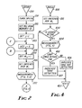
- a calibration routine is carried out which serves to establish which of the switches 2-8 are to be operated to cause the tone decoder to operate at the closest center frequency for each of the six tones that will be detected at various times.
- the appropriate combination of switch settings are obtained from the RAM 46 and used to connect resistors 12-18 in parallel with resistor 11 per the switch settings to cause the tone decoder 20 to free run near the frequency of the tone that is to be detected.
- the circuitry carries out a measurement routine which determines whether the frequency measured is higher or lower than the nominal value per the frequency measurement table stored in the ROM 44 for the tone that us sought and whether the measured frequency is within the bandwidth prescribed per the frequency measurement table stored in the ROM 44 for the tone being sought. Once the tone that is sought is detected, such detection is utilized to cause the operation of the facsimile machine to proceed to the next phase of its procedure at which time another of the six tones may be sought.
- the manufacturer's specifications for an NE567 tone decoder indicate that the center frequency where R is the total resistance presented between the capacitance 26 and the toner decoder 20 of Figure 1 and C is the capacitance presented by capacitor 26 of Figure 1.
- the manufacturer's specifications also indicate the range of R that can be used, for example, the range of R may be 2k ⁇ R ⁇ 20k ohms.
- the value for capacitor 26 is selected using the value of the maximum R allowed and the minimum center frequency for the range of tones of interest such that
- the process is repeated until all of the resistors 12-18 have been tried for each frequency.
- Information reflecting the combinations of the resistors 12-18 that are required for the six tones are stored in the RAM 46.
- An 8-byte memory location in the RAM 46 is used for each tone to be detected. This location is used to hold the on/off status for the seven switches 2-8 for each particular phase locked loop center frequency.
- the sole purpose of the calibration routine is to determine the switch settings for switches 2-8 for each of the tones to be detected and to store them. Assuming that M1-M6 are the six memory locations corresponding to the tones 1100, 1300, 1650, 1850, 2100, and 2400 HZ, respectively, and that each bit and each location corresponds to a switch setting.
- the circuitry With the 42 bits (6 tones, 7 bits per tone) determined by the calibration routine, the circuitry is then in condition to carry out the task of tone detection.
- the program for the microprocessor which is stored in the ROM 44, identifies which tone is to be sought causing the calibration information to be used for the selective operation of switches 2-8 to connect the required resistors of resistor 12-18 in parallel with resistor 11.
- the tone detector 20 responds to a tone that fall within the bandwidth of the tone decoder 20, the tone decoder 20 will lock on that tone, provide a locked output to the interface adapter 48 and initiate a measurement of the tone to which the tone decoder is locked. Once the measurement has been made, the measured frequency is compared with the frequency measurement table stored in the ROM 44 and if it is found to be within the prescribed bandwidth, the tone that was sought is considered detected.
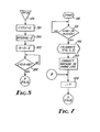
- the flow diagram requires that a determination be made when the count for the counter used to count the number of cycles of the signal provided by the tone decoder 20 reaches 128.
- the number of 256 microsecond intervals determined by the interval counter at the time the cycle count reaches 128 is a measure of the frequency.
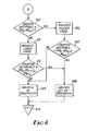
- This measured value for the frequency is used at step 305 in Figure 6 together with the frequency measurement table in the ROM 44 for determining whether the counted intervals is less than the number of intervals indicated by the first two entries in the ROM 44 for the frequency being calibrated, i.e., 1100 HZ.
- step 307 if the counted intervals is less than the number of intervals for the desired frequency per the frequency measurement table in ROM 44 when reduced by the bandwidth as stored in the frequency measurement table an indication will be given at step 308 that the measured frequency is out of bandwidth. Otherwise, an indication will be given at step 309 that the measured frequency is within the bandwidth per the frequency measurement table of ROM 44.
- step 310 if the counted intervals were greater than the number of intervals as set forth in the frequency measurement table in ROM 44, step 310 would indicate the measured frequency was lower than that per the frequency measurement table information. In this case, a determination is also made as to whether the measured frequency is within or outside the bandwidth per the frequency measurement table in ROM 44.
- Such a determination is indicated at step 311 with the out of bandwidth indication, when pertinent, given at step 308 and the in bandwidth indication, when present, given at step 309.
- the measurement routine is exited as indicated at 312.
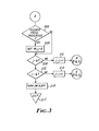
- Figure 2 indicates that the calibration routine is continued at Figure 3.
- the indication established at 306 or 310 in connection with the measurement routine set forth in Figure 6 as to whether the measured frequency is higher or lower than the frequency being calibrated is utilized at step 208 in Figure 3 where query is made as to whether a higher frequency is indicated.
- step 210 If it had been found that the measured frequency was greater than the frequency per the frequency measurement table in ROM 44 for the frequency under consideration, i.e., a higher frequency indication is present, the memory position M 12 , which had been made equal to 1, at step 205 of Fig. 2, would be changed to 0 before proceeding to step 210.
- the step for setting memory position M12 to 0 is indicated at 209. Since it will be determined at step 210 that j is not equal to 8, the flow diagram proceeds to step 211 where a new j is determined by adding one to the old value for j. For the procedure described to this point, the new j is 3. Return is then made to step 205 of the flow diagram set forth in Figure 2.
- the memory position M 13 is set equal to 1.
- the switches 2-8 are set per the memory position M 1 in the RAM 46.
- the memory bit position M13 set equal to 1 at this point in the calibration only switch 3 is turned on to connect resistor 13 in parallel with resistor 11.
- a measurement per step 207 is then made of the frequency provided by the tone decoder 20. The measurement procedure is then carried out in accordance with flow diagrams set forth in Figures 5 and 6 which have already been described and upon completion of the measurement step 207, the calibration procedure as has been described in connection with Figure 3 is continued.
- the flow diagram takes us to step 213 where a new i is established which is equal to the old i plus 1.
- the operation of the circuitry then proceeds according to the flow diagram of Figure 2 at step 204 which requires the setting of j equal to 2.
- the memory position and bit position within that memory which in this case is memory position M 22 , is set equal to 1 at step 205.
- the calibration procedure then proceeds as before except in this case i equals 2, so the bits for the new memory position M 2 , which is the calibration memory position for the second tone, i.e. 1300 HZ, will be determined.
- step 212 in Figure 3 the query made at step 212 as to whether i equals 6 will be answered in the affirmative, causing the operation to proceed to step 214 which serves to turn off switch 9.
- the routine of Figure 3 is then exited at step 215. With switch 9 off, the circuitry in condition for receiving a tone input to tone decoder 20 via resistor 30 and capacitor 32. With the calibration procedure called for at step 102 of the flow diagram of Figure 7 completed, the next step 103 in Figure 7 which calls for connection of a facsimile machine to the phone line, is completed.
- the tone detection circuitry of Figure 1 is controlled so that it will try to detect one of the tones for a short period of time, and if such tone is not detected in such time, it is then conditioned to detect the other tone for the same period of time. If the second tone is not detected, the procedure is repeated until one of the two tones is detected.
- step 104 is next which establishes tone 3 (1650 HZ) as the tone to be detected.
- the flow diagram is then continued at Figure 8 where a time period of half a second is started as indicated at step 105.
- the detection procedure at step 106 which is set forth in more detail at Figure 4, is entered. Such detection procedure will not be discussed at this time.
- step 107 a determination is made at step 107 as to whether the tone sought was detected during the detection routine. If the tone sought has been detected, step 108, which calls for the starting of the facsimile machine, is completed.
- the procedure for transmitting the document is then initiated as indicated at step 109.
- the procedure set forth in Figure 8 at 105 is then again entered and is carried out as has been described until such time as either tone 3 (1650 HZ) or tone 4 (1850 HZ) is detected.
- step 107 indicates a tone has been detected
- the machine start step 108 and transmit step 109 will follow.
- Other procedures relating to the further operation of the facsimile machine may call for other tones of the remaining four tones to be detected. Such procedures are not considered and as they would not contribute to the description already given for the operation of the tone detection circuitry of Figure 1
- the next step 401 calls for the setting of switches 2-8 of Figure 1 in accordance with the calibration information that was recorded in RAM 46 during the calibration procedure for the tone that is sought to be detected. Thus, if tone 3 (1650 HZ) is being sought the switches 2-8 are set according to the information at memory location M 3 in RAM 46.
- the next step 402 is a determination as to whether a locked output is present at conductor 50 from tone decoder 20.
- a locked output it is an indication that the tone decoder 20 detected a tone at its input that is within the bandwidth of the tone decoder 20. If a locked output is not present, the detection routine is exited as indicated at 403. If the locked output 50 is active, the measurement procedure as indicated at 404 and set forth in Figure 5 and 6 and which has been previously described, is entered. The measurement procedure will provide an indication as to whether the measured signal is within or outside of the bandwidth required for the frequency measurement table stored in the ROM 44. The step 405 of the detection routine per Figure 4, which follows the measurement procedures, calls for a determination as to whether the frequency measured is within the bandwidth.
- step 406 If it is not within the bandwidth, an indication that a tone is not detected is provided at step 406 and the routine is exited as indicated at step 403. If it is within the bandwidth, step 407 is entered which provides an indication that the tone sought is detected and the detection routine is then exited as indicated at step 403.
- resistors 12-18 of Figure 1 are required to be arranged in order of increasing magnitude, the values of resistors 12-18 in ohms are as follows:
- timing capacitance 26 and timing resistance 28 sets forth two ways for changing the product of the timing capacitance 26 and timing resistance 28, i.e., by the use of a fixed capacitance in series with a plurality of resistors selectively connectable in parallel or a fixed resistor in series with plurality of capacitors selectively connectable in parallel. It is apparent to those of ordinary skill in the art that there are many ways of altering the product of the timing capacitance 26 and timing resistance 28. For example, using a fixed capacitance 26, the timing resistance 28 can be varied by the use of a plurality of resistors connected in series, which are selectively shorted out by a switch provided for each resistor.
- a fixed resistor could be connected in series with a plurality of series connected capacitors which are selectively shorted out by a switch provided for each capacitor.
- a plurality of capacitors and a plurality of resistors could be used in various series/parallel arrangements with switches provided for making selective connections to vary the product of the timing resistance and timing capacitance.
Landscapes
- Physics & Mathematics (AREA)
- General Physics & Mathematics (AREA)
- Nonlinear Science (AREA)
- Measurement Of Resistance Or Impedance (AREA)
- Digital Transmission Methods That Use Modulated Carrier Waves (AREA)
Claims (5)
Applications Claiming Priority (2)
| Application Number | Priority Date | Filing Date | Title |
|---|---|---|---|
| US06/249,882 US4370650A (en) | 1981-04-01 | 1981-04-01 | Tone detection circuitry |
| US249882 | 1988-09-27 |
Publications (2)
| Publication Number | Publication Date |
|---|---|
| EP0061853A1 EP0061853A1 (de) | 1982-10-06 |
| EP0061853B1 true EP0061853B1 (de) | 1985-03-13 |
Family
ID=22945412
Family Applications (1)
| Application Number | Title | Priority Date | Filing Date |
|---|---|---|---|
| EP82301246A Expired EP0061853B1 (de) | 1981-04-01 | 1982-03-11 | Tondetektorschaltung |
Country Status (5)
| Country | Link |
|---|---|
| US (1) | US4370650A (de) |
| EP (1) | EP0061853B1 (de) |
| JP (1) | JPS57176869A (de) |
| DE (1) | DE3262513D1 (de) |
| MX (1) | MX152063A (de) |
Families Citing this family (8)
| Publication number | Priority date | Publication date | Assignee | Title |
|---|---|---|---|---|
| US4459672A (en) * | 1980-02-27 | 1984-07-10 | Regency Electronics, Inc. | Decoder |
| US4502049A (en) * | 1982-08-30 | 1985-02-26 | Itec, Inc. | Universal signalling tone receiver |
| US4818989A (en) * | 1984-03-27 | 1989-04-04 | Rockwell International Corporation | Selective calling decoder |
| JPS6152038A (ja) * | 1984-08-22 | 1986-03-14 | Nec Corp | 無線選択呼出受信機 |
| US5583785A (en) * | 1993-12-28 | 1996-12-10 | Talkie Tooter, Inc. | Method and apparatus for signal decoder using instantaneous magnitude and phase detection |
| US5546025A (en) * | 1994-03-11 | 1996-08-13 | Mitel, Inc. | Low frequency discrimator using upper and lower thresholds |
| US5915029A (en) * | 1998-04-23 | 1999-06-22 | Sony Corporation | Automated testing apparatus for electronic component |
| US12284000B2 (en) * | 2021-10-14 | 2025-04-22 | Centurylink Intellectual Property Llc | Easy DSL signal detector |
Family Cites Families (8)
| Publication number | Priority date | Publication date | Assignee | Title |
|---|---|---|---|---|
| US3593151A (en) * | 1968-08-12 | 1971-07-13 | Xerox Corp | Detector for receiver printer startup |
| US3922611A (en) * | 1973-11-23 | 1975-11-25 | Xerox Corp | Facsimile carrier detect circuit |
| US3952288A (en) * | 1974-09-30 | 1976-04-20 | Bell & Howell Company | Multifrequency linear filter networks with active elements |
| GB2001190A (en) * | 1977-07-12 | 1979-01-24 | Dobbie J G | Automatic musical tuning device |
| US4208626A (en) * | 1978-03-06 | 1980-06-17 | Bunker Ramo Corporation | Precision timing source for multiple rate sampling of high-speed waveforms |
| US4236110A (en) * | 1978-06-29 | 1980-11-25 | E-Systems, Inc. | Digital frequency deviation meter |
| US4215308A (en) * | 1978-10-30 | 1980-07-29 | Hewlett-Packard Company | Self calibrating crystal controlled frequency counter method and apparatus |
| FR2485843B1 (fr) * | 1980-06-25 | 1986-11-07 | Cit Alcatel | Recepteur numerique de frequences |
-
1981
- 1981-04-01 US US06/249,882 patent/US4370650A/en not_active Expired - Lifetime
-
1982
- 1982-03-11 EP EP82301246A patent/EP0061853B1/de not_active Expired
- 1982-03-11 DE DE8282301246T patent/DE3262513D1/de not_active Expired
- 1982-03-31 JP JP57053625A patent/JPS57176869A/ja active Pending
- 1982-03-31 MX MX192070A patent/MX152063A/es unknown
Also Published As
| Publication number | Publication date |
|---|---|
| MX152063A (es) | 1985-05-27 |
| JPS57176869A (en) | 1982-10-30 |
| US4370650A (en) | 1983-01-25 |
| EP0061853A1 (de) | 1982-10-06 |
| DE3262513D1 (en) | 1985-04-18 |
Similar Documents
| Publication | Publication Date | Title |
|---|---|---|
| US4206449A (en) | Multiple sensor intrusion alarm system | |
| US4549044A (en) | Remote telemetry unit | |
| CA1227586A (en) | Call progress for a computer telephone interface | |
| US4370650A (en) | Tone detection circuitry | |
| US4706203A (en) | Capacitive gauging method and apparatus | |
| JP2508929B2 (ja) | 加熱調理装置における測温回路 | |
| EP0029673A1 (de) | Anlage zur Objekterkennung | |
| GB2075232A (en) | Sensor monitor system | |
| US4362988A (en) | Method of and circuit arrangement for determining the magnitude of an unknown resistance element | |
| GB1583508A (en) | Dialysis machine | |
| CN105973947A (zh) | 一种tds值的测量方法及测量系统 | |
| EP0622767B1 (de) | Wärmefühler | |
| US5168273A (en) | Sequential analog/digital data multiplexing system and method | |
| EP0388523A2 (de) | Anordnung zum Anzeigen der Restladung eines Akkumulators | |
| US7116159B2 (en) | Method and apparatus for adjusting an active filter | |
| US6438500B1 (en) | Method and device for detecting the absence of a product in a reservoir | |
| EP0785691B1 (de) | Signalerkennungsanordnung unter Verwendung von Kadenztabellen | |
| GB2112948A (en) | Telephone cable splicers test set and method of testing | |
| US4429271A (en) | Digital capacitance measuring test set and test circuit incorporated therein | |
| US4802167A (en) | Data monitor apparatus | |
| GB2066621A (en) | Telephone call charge monitor | |
| GB2111273A (en) | Multiple detector circuit | |
| JPS59128892A (ja) | 平衡回路網の自動可変方式 | |
| KR0136452B1 (ko) | 주파수 판별방법 | |
| JPH08214080A (ja) | 回線インターフェイス監視回路を具備した情報配信装置 |
Legal Events
| Date | Code | Title | Description |
|---|---|---|---|
| PUAI | Public reference made under article 153(3) epc to a published international application that has entered the european phase |
Free format text: ORIGINAL CODE: 0009012 |
|
| AK | Designated contracting states |
Designated state(s): DE FR GB |
|
| 17P | Request for examination filed |
Effective date: 19830330 |
|
| GRAA | (expected) grant |
Free format text: ORIGINAL CODE: 0009210 |
|
| AK | Designated contracting states |
Designated state(s): DE FR GB |
|
| REF | Corresponds to: |
Ref document number: 3262513 Country of ref document: DE Date of ref document: 19850418 |
|
| ET | Fr: translation filed | ||
| PLBE | No opposition filed within time limit |
Free format text: ORIGINAL CODE: 0009261 |
|
| PLBE | No opposition filed within time limit |
Free format text: ORIGINAL CODE: 0009261 |
|
| STAA | Information on the status of an ep patent application or granted ep patent |
Free format text: STATUS: NO OPPOSITION FILED WITHIN TIME LIMIT |
|
| 26N | No opposition filed | ||
| 26N | No opposition filed | ||
| PGFP | Annual fee paid to national office [announced via postgrant information from national office to epo] |
Ref country code: FR Payment date: 19890124 Year of fee payment: 8 |
|
| PGFP | Annual fee paid to national office [announced via postgrant information from national office to epo] |
Ref country code: DE Payment date: 19890214 Year of fee payment: 8 |
|
| PGFP | Annual fee paid to national office [announced via postgrant information from national office to epo] |
Ref country code: GB Payment date: 19890228 Year of fee payment: 8 |
|
| REG | Reference to a national code |
Ref country code: GB Ref legal event code: 732 |
|
| PG25 | Lapsed in a contracting state [announced via postgrant information from national office to epo] |
Ref country code: GB Effective date: 19900311 |
|
| GBPC | Gb: european patent ceased through non-payment of renewal fee | ||
| PG25 | Lapsed in a contracting state [announced via postgrant information from national office to epo] |
Ref country code: FR Effective date: 19901130 |
|
| PG25 | Lapsed in a contracting state [announced via postgrant information from national office to epo] |
Ref country code: DE Effective date: 19901201 |
|
| REG | Reference to a national code |
Ref country code: FR Ref legal event code: ST |