EP0063407A1 - Système détecteur d'erreur de connexion de circuit logique - Google Patents
Système détecteur d'erreur de connexion de circuit logique Download PDFInfo
- Publication number
- EP0063407A1 EP0063407A1 EP82301143A EP82301143A EP0063407A1 EP 0063407 A1 EP0063407 A1 EP 0063407A1 EP 82301143 A EP82301143 A EP 82301143A EP 82301143 A EP82301143 A EP 82301143A EP 0063407 A1 EP0063407 A1 EP 0063407A1
- Authority
- EP
- European Patent Office
- Prior art keywords
- comparator
- output
- logic circuit
- input
- voltage level
- Prior art date
- Legal status (The legal status is an assumption and is not a legal conclusion. Google has not performed a legal analysis and makes no representation as to the accuracy of the status listed.)
- Granted
Links
Images

Classifications
-
- G—PHYSICS
- G06—COMPUTING OR CALCULATING; COUNTING
- G06F—ELECTRIC DIGITAL DATA PROCESSING
- G06F11/00—Error detection; Error correction; Monitoring
- G06F11/07—Responding to the occurrence of a fault, e.g. fault tolerance
- G06F11/0703—Error or fault processing not based on redundancy, i.e. by taking additional measures to deal with the error or fault not making use of redundancy in operation, in hardware, or in data representation
- G06F11/0751—Error or fault detection not based on redundancy
- G06F11/0754—Error or fault detection not based on redundancy by exceeding limits
-
- G—PHYSICS
- G01—MEASURING; TESTING
- G01R—MEASURING ELECTRIC VARIABLES; MEASURING MAGNETIC VARIABLES
- G01R31/00—Arrangements for testing electric properties; Arrangements for locating electric faults; Arrangements for electrical testing characterised by what is being tested not provided for elsewhere
- G01R31/28—Testing of electronic circuits, e.g. by signal tracer
- G01R31/317—Testing of digital circuits
- G01R31/3181—Functional testing
- G01R31/3185—Reconfiguring for testing, e.g. LSSD, partitioning
- G01R31/318505—Test of Modular systems, e.g. Wafers, MCM's
-
- G—PHYSICS
- G01—MEASURING; TESTING
- G01R—MEASURING ELECTRIC VARIABLES; MEASURING MAGNETIC VARIABLES
- G01R31/00—Arrangements for testing electric properties; Arrangements for locating electric faults; Arrangements for electrical testing characterised by what is being tested not provided for elsewhere
- G01R31/50—Testing of electric apparatus, lines, cables or components for short-circuits, continuity, leakage current or incorrect line connections
- G01R31/66—Testing of connections, e.g. of plugs or non-disconnectable joints
- G01R31/70—Testing of connections between components and printed circuit boards
-
- G—PHYSICS
- G06—COMPUTING OR CALCULATING; COUNTING
- G06F—ELECTRIC DIGITAL DATA PROCESSING
- G06F11/00—Error detection; Error correction; Monitoring
- G06F11/22—Detection or location of defective computer hardware by testing during standby operation or during idle time, e.g. start-up testing
- G06F11/2205—Detection or location of defective computer hardware by testing during standby operation or during idle time, e.g. start-up testing using arrangements specific to the hardware being tested
- G06F11/2221—Detection or location of defective computer hardware by testing during standby operation or during idle time, e.g. start-up testing using arrangements specific to the hardware being tested to test input/output devices or peripheral units
Definitions
- This invention relates to logic circuit interconnect fault detection systems which can be incorporated into individual integrated circuit chips.
- a fault detection system of the present invention can detect internal as well as interconnect faults of various types between integrated circuit chips.
- a particular application of the present invention is as an interconnect fault detection system for large-scale integrated circuit (LSI) chips and the interconnect system connecting a plurality of such chips.
- LSI large-scale integrated circuit
- interconnect fault detection system is a current focus of attention for fault reliability or fault detection. Because of increasing use pressure to improve reliability of products incorporating such chips, a means of detecting a substantial number of the interconnect related failures in a system is required. Thus a primary goal of an interconnect fault detection system is that it can operate simultaneously and continuously with the intended normal circuit operations and functions.
- a logic circuit interconnect fault detection system characterised by comprising: a first logic circuit chip containing logic circuits connected with input and output pins; at least one voltage level sensing circuit on said first logic circuit chip associated with one of the said input and output pins; a comparator on said first logic circuit chip connected with the output of said at least one voltage level sensing circuit the output of said comparator being connected to an output pin of said first logic circuit chip, said comparator output being a fault indication signal; a second logic circuit chip containing logic circuits connected with input and output pins; at least one voltage level sensing circuit on said second logic circuit chip associated with one of the input or output pins; a comparator on said second logic circuit chip connected with the output of said at least one voltage level sensing circuit and the output of said comparator connected to an output pin of said second logic circuit chip said comparator output being a fault indication signal; a plurality of interconnect means between particular input and output pins of said first and second chips, including at least one pin on each chip having
- a fault indication signal is generated.
- An open circuit anywhere in the interconnect systems will cause some number of input/output pins, dependent on the fault location, to be pulled towards a voltage outside of the normal operating range as a result of the impedance of the level sensor. This condition is reported as a fault.
- any short to ground condition within the interconnect network will cause a voltage shift which will be reported as a fault detected.
- Certain types of interconnect faults which result from a high impedance connection will cause a "ringing" signal in the interconnect network.
- This ringing signal can be detected frequently if any peak of the ringing voltage falls outside the threshold range and causes actuation of the comparator. This typically occurs with the most significant interconnect faults having the greatest impedance mismatch and therefore the greatest likelihood of producing error signals in the interconnect system.
- a particular advantage of the present invention is that the same level sensor circuit may be used with both input pins and output pins.
- the fault detection system may be designed on a gate array type chip base where particular chips may vary as to individual pin functions.
- the chips involved can be determined, which in many cases determines the particular interconnect system having an error.
- the number of comparators per chip and the number of fault output detect lines per chip where each comparator will receive level sensor signals from fewer input/output pins on each chip a more complex pattern of fault detection signals can be created which will more nearly determine the location of any particular fault.
- the system could be generated in an embodiment so as to have an individual comparator for each level sensor and input/output pin combination.
- comparators could be connected through level shifters to drive a light emitting diode (LED) to provide a visible indication of a fault for troubleshooting.
- LED light emitting diode
- various combinations of intensity of interconnect fault detection can be provided in any system depending upon the criticality of that system. Therefore, it is possible that a given computer might have different levels of interconnect fault detection in different portions of the computer.
- an interconnect fault detection system characterised by comprising: a plurality of circuit boards each containing a plurality of logic chips each of which contains a level sensor and comparator for each input and output pin so that each chip has at least one fault indication output; an OR means on each board connecting all of the fault indicating outputs on the board to at least one OR gate which provides a fault indication for the particular board; a pulse catcher means connected to the individual fault outputs of each logic board; a status register connected with the output of the pulse catcher; and a maintenance system providing for diagnostic surveillance of the circuit boards so that the status register will give an individual unique indication for each circuit board having an output fault indication.
- a logic circuit chip fault detection system for use with an operatively connected logic circuit chip at the same time said logic circuit chip is in use, characterised by comprising: a plurality of individual voltage level sensing circuits of common configuration, one of said voltage level sensing circuits being provided for each of the input and output pins on said logic circuit chip; at least one voltage comparator on said chip, said voltage comparator being connected with a plurality of voltage level sensing circuits, said chip having every voltage level sensing circuit connected with a voltage comparator; a reference voltage input to said voltage comparator so that if any voltage level sensing circuit associated with said comparator detects a voltage outside of the voltage threshold set by said reference voltage, said comparator produces a signal representative of a fault indication.
- ECL emitter coupled logic
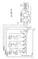
- a logic chip 12 contains a number of input/output pins 14, 16 and so forth up to the Nth pin 18.
- Each input or output pin is associated with an individual voltage level sensor.
- the input/output pin 14 is associated with a voltage level sensor 19 which contains an internal impedance 20 which may be in the form of a simple resistor.
- the impedance 20 is connected to ground reference L, from the input/output pin.
- the normal, logic external output to the pin is shown in the general sense as an emitter coupled transistor 22 which receives a logic input signal 24.
- the level sensor 19 also includes a transistor 26 having its base connected to an interconnect logic level and its collector connected to ground reference L 1*
- the emitter of the transistor 26 is connected to a fault detection logic bus 28 which is similarly connected to other level sensors 30, 32 on the logic chip. These level sensors 30, 32 are associated with pins each of which has a normal logic connection 34, 36, respectively.
- the bus 28 is shown connected with N different input/output connections.
- the bus is provided as the compare input to a comparator 40.
- a detection threshold voltage input 42 is provided as the reference input to the comparator.
- An output interconnect pin 44 of the comparator carries a fault report output signal.
- connection bus 56 for a particular pin interconnect combination.
- the interconnect bus 56 has a termination impedance 58 which may be a resistor.
- the termination impedance is reference to a voltage level which, for example, in this case may be -2 volts.
- the chip 50 similarly has conventional internal logic gates shown representatively by a gate 60 of the type to be associated in this logic system. Similarly,level sensors are provided for each input and output pin on the chips 50, 52, 54.
- a level sensor 62 similar to level sensor 19, has an internal impedance 64 and a transistor gate 66, provides an output level sensing signal to a fault detection bus 68.
- a comparator 70 provides a fault detection output.
- the other logic chips 52, 54 are similar.
- the bus 56 is comprised of a controlled impedance path containing connectors, coax cable, printed circuit strip lines or twisted pair connections to interconnect various logic chips.
- the termination impedance 58 is provided to be essentially equal to the path impedance so that impedance is properly matched throughout the circuit.
- the failure modes of these types of interconnects and logic systems is typically that'of .-an open circuit or of a short to ground. If any interconnect components, including the termination impedance either opens or shorts to ground, a non- logic voltage level will appear on the interconnection path which will be detected by one or more of the monitoring circuits. Because of the high number of gates as compared to the number of input/output pins of LSI circuits, this can be a very economical and effective technique of fault detection and isolation.
- Normal logic levels in a typical ECL logic system are in the range of -.7 to -1.8 volts.
- An open circuit anywhere in the interconnect network will cause some number of chip pins, dependent on the fault location, to be pulled towards zero volts by the impedances, such as 20 and 64, in each level sensor. This condition is sensed by comparison against a detection threshold voltage and reported by comparators, such as 40 and 70. Any short to ground condition causes a similar voltage shift and is detected in the same way.
- Interconnect faults of the sort which cause a large impedance mismatch and therefore a ringing signal when the signal crosses the impedance mismatched path, will also be detected if the peak voltage of the ringing oscillation signal exceeds the threshold voltage.
- the normal range of voltages in an ECL logic circuit is shown as having a lower level 100, an upper level 102 and an error threshold level of 104.
- a ground short circuit level will produce a zero volt signal on interconnect path at 106, above the threshold voltage.
- an open circuit someplace in the interconnect path will produce an open level voltage 108 at some voltage outside the threshold voltage level but different from zero volts.
- a ringing signal caused by an impedance mismatch in the interconnect path is shown, for example, at 110 where the peaks of the ringing signal cross the error threshold voltage level 104 to cause a fault detection condition.
- FIG. 3 a complete system of the sort which might be found in a large digital computer is shown having a number N of circuit boards 120, 122, 124. Each board contains a number of logic chips 126, 128, 130, 132, 134 up to an Nth chip 136.
- the output of each individual chip on a circuit board is provided to an LED 140, 142, 144, 146, 148, 150, respectively.
- the LED s are supplied with a supply voltage on a supply bus 152 from a voltage source.
- the supply bus is connected with a level shifting circuit 154.
- the level shifting circuit works with the OR function generated by the LEDs to produce an output signal if any one of the chips on the circuit board has a fault.
- the LEDs naturally provide an OR function as any conventional diode does.
- Individual outputs from the individual circuit boards are connected to individual inputs to a pulse catcher network 160 which in turn provides an output to a status register 162.
- the status register provides an output 164 to computer maintenance software and display system schematically shown as 166.
- a given chip on a given circuit board has a fault, it will light its associated LED and produce an output pulse for the board. This output pulse will pass into the pulse catcher which will identify on the status register the particular board having a fault.
- a maintenance person will locate the appropriate board in the computer and note on the board the particular LED which is giving a fault indication and in that way readily find a given logic chip which needs to be replaced or which needs to have its interconnect network serviced. If a plurality of circuit boards and chips simultaneously have a fault condition detected, a proper diagnostic approach could clearly accomplish a great deal towards showing the specific pin interconnect system at fault.
Landscapes
- Engineering & Computer Science (AREA)
- Physics & Mathematics (AREA)
- General Physics & Mathematics (AREA)
- General Engineering & Computer Science (AREA)
- Theoretical Computer Science (AREA)
- Quality & Reliability (AREA)
- Tests Of Electronic Circuits (AREA)
- Logic Circuits (AREA)
- Testing Or Measuring Of Semiconductors Or The Like (AREA)
- Semiconductor Integrated Circuits (AREA)
Applications Claiming Priority (2)
| Application Number | Priority Date | Filing Date | Title |
|---|---|---|---|
| US255929 | 1981-04-20 | ||
| US06/255,929 US4395767A (en) | 1981-04-20 | 1981-04-20 | Interconnect fault detector for LSI logic chips |
Publications (2)
| Publication Number | Publication Date |
|---|---|
| EP0063407A1 true EP0063407A1 (fr) | 1982-10-27 |
| EP0063407B1 EP0063407B1 (fr) | 1986-11-12 |
Family
ID=22970433
Family Applications (1)
| Application Number | Title | Priority Date | Filing Date |
|---|---|---|---|
| EP82301143A Expired EP0063407B1 (fr) | 1981-04-20 | 1982-03-05 | Système détecteur d'erreur de connexion de circuit logique |
Country Status (6)
| Country | Link |
|---|---|
| US (1) | US4395767A (fr) |
| EP (1) | EP0063407B1 (fr) |
| JP (1) | JPS57180140A (fr) |
| AU (1) | AU551062B2 (fr) |
| CA (1) | CA1181531A (fr) |
| DE (1) | DE3274300D1 (fr) |
Cited By (1)
| Publication number | Priority date | Publication date | Assignee | Title |
|---|---|---|---|---|
| EP0479515A3 (fr) * | 1990-10-01 | 1994-10-12 | Motorola Inc | Circuit pour détecter des défauts. |
Families Citing this family (31)
| Publication number | Priority date | Publication date | Assignee | Title |
|---|---|---|---|---|
| US4494066A (en) * | 1981-07-02 | 1985-01-15 | International Business Machines Corporation | Method of electrically testing a packaging structure having n interconnected integrated circuit chips |
| US4504784A (en) * | 1981-07-02 | 1985-03-12 | International Business Machines Corporation | Method of electrically testing a packaging structure having N interconnected integrated circuit chips |
| JPS58115372A (ja) * | 1981-12-29 | 1983-07-09 | Fujitsu Ltd | 半導体装置試験回路 |
| US4509008A (en) * | 1982-04-20 | 1985-04-02 | International Business Machines Corporation | Method of concurrently testing each of a plurality of interconnected integrated circuit chips |
| US4660198A (en) * | 1985-04-15 | 1987-04-21 | Control Data Corporation | Data capture logic for VLSI chips |
| JPH01154546A (ja) * | 1987-12-10 | 1989-06-16 | Fujitsu Ltd | 端子開放検出回路半導体装置 |
| JPH0255355U (fr) * | 1988-10-11 | 1990-04-20 | ||
| US5070296A (en) * | 1990-06-22 | 1991-12-03 | Honeywell Inc. | Integrated circuit interconnections testing |
| WO1992013281A1 (fr) * | 1991-01-22 | 1992-08-06 | Vlsi Technology, Inc. | Procede de reduction des vecteurs et du temps de controle dans des dispositifs utilisant des blocs equivalents |
| JP2884847B2 (ja) * | 1991-10-03 | 1999-04-19 | 三菱電機株式会社 | 故障検出機能を備えた半導体集積回路装置の製造方法 |
| US5278841A (en) * | 1991-10-30 | 1994-01-11 | International Business Machines Corporation | Method and apparatus for diagnosing net interconnect faults using echo pulsed signals |
| JP3377225B2 (ja) * | 1992-04-07 | 2003-02-17 | 富士写真フイルム株式会社 | チェック回路を含む集積回路 |
| US5581176A (en) * | 1993-05-24 | 1996-12-03 | North American Philips Corporation | Analog autonomous test bus framework for testing integrated circuits on a printed circuit board |
| GB2278689B (en) * | 1993-06-02 | 1997-03-19 | Ford Motor Co | Method and apparatus for testing integrated circuits |
| JPH07167920A (ja) * | 1993-10-18 | 1995-07-04 | Fujitsu Ltd | Lsi |
| FR2732133B1 (fr) * | 1995-03-21 | 1997-04-25 | Sgs Thomson Microelectronics | Detecteur de coherence d'informations contenues dans un circuit integre |
| DE19723079C1 (de) * | 1997-06-02 | 1998-11-19 | Bosch Gmbh Robert | Fehlerdiagnosevorrichtung und -verfahren |
| JP3361472B2 (ja) * | 1999-04-02 | 2003-01-07 | 松下電器産業株式会社 | アナログ・バウンダリ・スキャン対応集積回路装置 |
| US6804803B2 (en) | 2001-04-05 | 2004-10-12 | International Business Machines Corporation | Method for testing integrated logic circuits |
| US7049842B2 (en) * | 2003-12-18 | 2006-05-23 | Texas Instruments Incorporated | Simultaneous pin short and continuity test on IC packages |
| JP4315853B2 (ja) * | 2004-04-08 | 2009-08-19 | 富士通株式会社 | Icカード機能を有した携帯機器 |
| JP4692255B2 (ja) * | 2005-12-02 | 2011-06-01 | 株式会社デンソー | 断線検出装置 |
| US9363469B2 (en) | 2008-07-17 | 2016-06-07 | Ppc Broadband, Inc. | Passive-active terminal adapter and method having automatic return loss control |
| JP2012078332A (ja) * | 2009-10-09 | 2012-04-19 | Elpida Memory Inc | 半導体装置、半導体装置の試験方法、及びデータ処理システム。 |
| US8699356B2 (en) * | 2010-12-20 | 2014-04-15 | Deere & Company | Method and system for diagnosing a fault or open circuit in a network |
| TWI477788B (zh) * | 2012-04-10 | 2015-03-21 | Realtek Semiconductor Corp | 偵測發光二極體短路的方法及其裝置 |
| FR3090888B1 (fr) * | 2018-12-19 | 2020-11-27 | Continental Automotive France | Dispositif de détection automatique de couplage entre dispositifs électronique |
| CN111458621B (zh) * | 2019-01-21 | 2022-03-01 | 华邦电子股份有限公司 | 集成电路及其多芯片状态的检测方法 |
| CN110297737B (zh) * | 2019-07-10 | 2023-11-14 | 北京汽车股份有限公司 | 多路输出芯片的故障诊断测试方法及装置 |
| CN116256615B (zh) * | 2023-01-29 | 2026-04-21 | 苏州元脑智能科技有限公司 | 芯片检测方法和设备、存储介质及电子装置 |
| CN119355587B (zh) * | 2024-12-23 | 2025-04-04 | 芯洲科技(北京)股份有限公司 | 芯片引脚的连接器件的检测方法及电路 |
Citations (3)
| Publication number | Priority date | Publication date | Assignee | Title |
|---|---|---|---|---|
| US3746973A (en) * | 1972-05-05 | 1973-07-17 | Ibm | Testing of metallization networks on insulative substrates supporting semiconductor chips |
| US3784910A (en) * | 1972-07-13 | 1974-01-08 | Teradyne Inc | Sequential addressing network testing system |
| GB1555026A (en) * | 1976-04-03 | 1979-11-07 | Ibm | Circuit testing apparatus |
Family Cites Families (10)
| Publication number | Priority date | Publication date | Assignee | Title |
|---|---|---|---|---|
| DE1951861A1 (de) * | 1968-10-17 | 1970-08-06 | Gen Electric Information Syste | Verfahren und Anordnung zur automatischen UEberpruefung von Karten mit gedruckten Schaltungen |
| US3851161A (en) * | 1973-05-07 | 1974-11-26 | Burroughs Corp | Continuity network testing and fault isolating |
| US4001818A (en) * | 1975-10-22 | 1977-01-04 | Storage Technology Corporation | Digital circuit failure detector |
| US4009437A (en) * | 1976-03-31 | 1977-02-22 | Burroughs Corporation | Net analyzer for electronic circuits |
| US4183460A (en) * | 1977-12-23 | 1980-01-15 | Burroughs Corporation | In-situ test and diagnostic circuitry and method for CML chips |
| US4176258A (en) * | 1978-05-01 | 1979-11-27 | Intel Corporation | Method and circuit for checking integrated circuit chips |
| US4233682A (en) * | 1978-06-15 | 1980-11-11 | Sperry Corporation | Fault detection and isolation system |
| US4220917A (en) * | 1978-07-31 | 1980-09-02 | International Business Machines Corporation | Test circuitry for module interconnection network |
| US4241307A (en) * | 1978-08-18 | 1980-12-23 | International Business Machines Corporation | Module interconnection testing scheme |
| US4271515A (en) * | 1979-03-23 | 1981-06-02 | John Fluke Mfg. Co., Inc. | Universal analog and digital tester |
-
1981
- 1981-04-20 US US06/255,929 patent/US4395767A/en not_active Expired - Fee Related
-
1982
- 1982-02-23 JP JP57028037A patent/JPS57180140A/ja active Pending
- 1982-03-05 DE DE8282301143T patent/DE3274300D1/de not_active Expired
- 1982-03-05 EP EP82301143A patent/EP0063407B1/fr not_active Expired
- 1982-03-26 AU AU81977/82A patent/AU551062B2/en not_active Ceased
- 1982-04-07 CA CA000400678A patent/CA1181531A/fr not_active Expired
Patent Citations (3)
| Publication number | Priority date | Publication date | Assignee | Title |
|---|---|---|---|---|
| US3746973A (en) * | 1972-05-05 | 1973-07-17 | Ibm | Testing of metallization networks on insulative substrates supporting semiconductor chips |
| US3784910A (en) * | 1972-07-13 | 1974-01-08 | Teradyne Inc | Sequential addressing network testing system |
| GB1555026A (en) * | 1976-04-03 | 1979-11-07 | Ibm | Circuit testing apparatus |
Non-Patent Citations (1)
| Title |
|---|
| IBM TECHNICAL DISCLOSURE BULLETIN, Vol. 22, No. 8B, January 1980, New York, J.D. BARNES: "Interconnection Test Arrangement" pages 3679 to 3680 * |
Cited By (1)
| Publication number | Priority date | Publication date | Assignee | Title |
|---|---|---|---|---|
| EP0479515A3 (fr) * | 1990-10-01 | 1994-10-12 | Motorola Inc | Circuit pour détecter des défauts. |
Also Published As
| Publication number | Publication date |
|---|---|
| US4395767A (en) | 1983-07-26 |
| DE3274300D1 (en) | 1987-01-02 |
| AU8197782A (en) | 1982-10-28 |
| EP0063407B1 (fr) | 1986-11-12 |
| JPS57180140A (en) | 1982-11-06 |
| CA1181531A (fr) | 1985-01-22 |
| AU551062B2 (en) | 1986-04-17 |
Similar Documents
| Publication | Publication Date | Title |
|---|---|---|
| EP0063407B1 (fr) | Système détecteur d'erreur de connexion de circuit logique | |
| KR0138114B1 (ko) | 집적 회로의 다중 전원 접속부 검사 방법 및 그 장치 | |
| US4689551A (en) | Testing wiring harnesses | |
| EP0305148B1 (fr) | Détermination de l'orientation des composants | |
| US5031073A (en) | Fault-isolating apparatus and method for connecting circuitry | |
| JPH04507139A (ja) | 電気負荷、その駆動及び関連する接続線の機能を監視する装置 | |
| EP0241270B1 (fr) | Circuit de surveillance autotesté | |
| US5633651A (en) | Automatic bidirectional indicator driver | |
| US5136280A (en) | Switch status indicator and self tester | |
| US4342112A (en) | Error checking circuit | |
| US4764759A (en) | Open circuit detector for differential encoder feedback | |
| US4348636A (en) | Integrated circuit tester | |
| US3381270A (en) | Error detection circuits | |
| EP0285789A2 (fr) | Circuit logique à défaut tolérant | |
| CN112631855A (zh) | 一种金手指连接状态监测方法及装置 | |
| US6157308A (en) | Detecting hidden faults in reliable power systems | |
| US4031461A (en) | Source related potential indicating continuity tester | |
| US5565766A (en) | Semiconductor circuit element device with arrangement for testing the device and method of test | |
| EP0117295A2 (fr) | Dispositif d'auto-vérification des circuits d'attaque hors-microplaquette d'un système de traitement de données | |
| US3590378A (en) | Fault-detecting monitor for integrated circuit units | |
| CN87108371A (zh) | 具有三态电路检验能力的计算机辅助探针 | |
| US7321948B1 (en) | Highly available system test mechanism | |
| US5446399A (en) | Method and structure for a fault-free input configuration control mechanism | |
| US3132304A (en) | Marginal checking system employing switch means for selective and simultaneous introduction of auxiliary parallel loads | |
| EP0214229B1 (fr) | Circuit logique a testabilite amelioree des contacts d'interconnexion defectueux |
Legal Events
| Date | Code | Title | Description |
|---|---|---|---|
| PUAI | Public reference made under article 153(3) epc to a published international application that has entered the european phase |
Free format text: ORIGINAL CODE: 0009012 |
|
| AK | Designated contracting states |
Designated state(s): DE FR GB |
|
| 17P | Request for examination filed |
Effective date: 19830106 |
|
| GRAA | (expected) grant |
Free format text: ORIGINAL CODE: 0009210 |
|
| AK | Designated contracting states |
Kind code of ref document: B1 Designated state(s): DE FR GB |
|
| ET | Fr: translation filed | ||
| REF | Corresponds to: |
Ref document number: 3274300 Country of ref document: DE Date of ref document: 19870102 |
|
| PLBE | No opposition filed within time limit |
Free format text: ORIGINAL CODE: 0009261 |
|
| STAA | Information on the status of an ep patent application or granted ep patent |
Free format text: STATUS: NO OPPOSITION FILED WITHIN TIME LIMIT |
|
| 26N | No opposition filed | ||
| PGFP | Annual fee paid to national office [announced via postgrant information from national office to epo] |
Ref country code: FR Payment date: 19890124 Year of fee payment: 8 |
|
| PGFP | Annual fee paid to national office [announced via postgrant information from national office to epo] |
Ref country code: DE Payment date: 19890214 Year of fee payment: 8 |
|
| PGFP | Annual fee paid to national office [announced via postgrant information from national office to epo] |
Ref country code: GB Payment date: 19890228 Year of fee payment: 8 |
|
| PG25 | Lapsed in a contracting state [announced via postgrant information from national office to epo] |
Ref country code: GB Effective date: 19900305 |
|
| GBPC | Gb: european patent ceased through non-payment of renewal fee | ||
| PG25 | Lapsed in a contracting state [announced via postgrant information from national office to epo] |
Ref country code: FR Effective date: 19901130 |
|
| PG25 | Lapsed in a contracting state [announced via postgrant information from national office to epo] |
Ref country code: DE Effective date: 19901201 |
|
| REG | Reference to a national code |
Ref country code: FR Ref legal event code: ST |