EP0063414A2 - Anordnung zum Ein-und Auskoppeln von Signalen in eine und aus einer Zweidrahtleitung - Google Patents
Anordnung zum Ein-und Auskoppeln von Signalen in eine und aus einer Zweidrahtleitung Download PDFInfo
- Publication number
- EP0063414A2 EP0063414A2 EP82301490A EP82301490A EP0063414A2 EP 0063414 A2 EP0063414 A2 EP 0063414A2 EP 82301490 A EP82301490 A EP 82301490A EP 82301490 A EP82301490 A EP 82301490A EP 0063414 A2 EP0063414 A2 EP 0063414A2
- Authority
- EP
- European Patent Office
- Prior art keywords
- filter
- impedance
- impedances
- subscriber line
- band
- Prior art date
- Legal status (The legal status is an assumption and is not a legal conclusion. Google has not performed a legal analysis and makes no representation as to the accuracy of the status listed.)
- Granted
Links
Images

Classifications
-
- H—ELECTRICITY
- H03—ELECTRONIC CIRCUITRY
- H03H—IMPEDANCE NETWORKS, e.g. RESONANT CIRCUITS; RESONATORS
- H03H7/00—Multiple-port networks comprising only passive electrical elements as network components
- H03H7/01—Frequency selective two-port networks
- H03H7/17—Structural details of sub-circuits of frequency selective networks
- H03H7/1741—Comprising typical LC combinations, irrespective of presence and location of additional resistors
- H03H7/175—Series LC in series path
-
- H—ELECTRICITY
- H03—ELECTRONIC CIRCUITRY
- H03H—IMPEDANCE NETWORKS, e.g. RESONANT CIRCUITS; RESONATORS
- H03H7/00—Multiple-port networks comprising only passive electrical elements as network components
- H03H7/01—Frequency selective two-port networks
- H03H7/0115—Frequency selective two-port networks comprising only inductors and capacitors
-
- H—ELECTRICITY
- H03—ELECTRONIC CIRCUITRY
- H03H—IMPEDANCE NETWORKS, e.g. RESONANT CIRCUITS; RESONATORS
- H03H7/00—Multiple-port networks comprising only passive electrical elements as network components
- H03H7/01—Frequency selective two-port networks
- H03H7/17—Structural details of sub-circuits of frequency selective networks
- H03H7/1741—Comprising typical LC combinations, irrespective of presence and location of additional resistors
- H03H7/1758—Series LC in shunt or branch path
-
- H—ELECTRICITY
- H03—ELECTRONIC CIRCUITRY
- H03H—IMPEDANCE NETWORKS, e.g. RESONANT CIRCUITS; RESONATORS
- H03H7/00—Multiple-port networks comprising only passive electrical elements as network components
- H03H7/46—Networks for connecting several sources or loads, working on different frequencies or frequency bands, to a common load or source
- H03H7/463—Duplexers
-
- H—ELECTRICITY
- H04—ELECTRIC COMMUNICATION TECHNIQUE
- H04L—TRANSMISSION OF DIGITAL INFORMATION, e.g. TELEGRAPHIC COMMUNICATION
- H04L27/00—Modulated-carrier systems
- H04L27/0002—Modulated-carrier systems analog front ends; means for connecting modulators, demodulators or transceivers to a transmission line
-
- H—ELECTRICITY
- H04—ELECTRIC COMMUNICATION TECHNIQUE
- H04M—TELEPHONIC COMMUNICATION
- H04M11/00—Telephonic communication systems specially adapted for combination with other electrical systems
- H04M11/06—Simultaneous speech and data transmission, e.g. telegraphic transmission over the same conductors
- H04M11/062—Simultaneous speech and data transmission, e.g. telegraphic transmission over the same conductors using different frequency bands for speech and other data
-
- H—ELECTRICITY
- H03—ELECTRONIC CIRCUITRY
- H03H—IMPEDANCE NETWORKS, e.g. RESONANT CIRCUITS; RESONATORS
- H03H7/00—Multiple-port networks comprising only passive electrical elements as network components
- H03H7/01—Frequency selective two-port networks
- H03H7/075—Ladder networks, e.g. electric wave filters
-
- H—ELECTRICITY
- H03—ELECTRONIC CIRCUITRY
- H03H—IMPEDANCE NETWORKS, e.g. RESONANT CIRCUITS; RESONATORS
- H03H7/00—Multiple-port networks comprising only passive electrical elements as network components
- H03H7/01—Frequency selective two-port networks
- H03H7/09—Filters comprising mutual inductance
-
- H—ELECTRICITY
- H03—ELECTRONIC CIRCUITRY
- H03H—IMPEDANCE NETWORKS, e.g. RESONANT CIRCUITS; RESONATORS
- H03H7/00—Multiple-port networks comprising only passive electrical elements as network components
- H03H7/01—Frequency selective two-port networks
- H03H7/17—Structural details of sub-circuits of frequency selective networks
- H03H7/1741—Comprising typical LC combinations, irrespective of presence and location of additional resistors
- H03H7/1775—Parallel LC in shunt or branch path
-
- H—ELECTRICITY
- H03—ELECTRONIC CIRCUITRY
- H03H—IMPEDANCE NETWORKS, e.g. RESONANT CIRCUITS; RESONATORS
- H03H7/00—Multiple-port networks comprising only passive electrical elements as network components
- H03H7/01—Frequency selective two-port networks
- H03H7/17—Structural details of sub-circuits of frequency selective networks
- H03H7/1741—Comprising typical LC combinations, irrespective of presence and location of additional resistors
- H03H7/1783—Combined LC in series path
-
- H—ELECTRICITY
- H03—ELECTRONIC CIRCUITRY
- H03H—IMPEDANCE NETWORKS, e.g. RESONANT CIRCUITS; RESONATORS
- H03H7/00—Multiple-port networks comprising only passive electrical elements as network components
- H03H7/42—Networks for transforming balanced signals into unbalanced signals and vice versa, e.g. baluns
- H03H7/425—Balance-balance networks
Definitions
- This invention relates to filters comprising reactive components, and to a method of determining impedances of such components.
- the invention is particularly, but not exclusively, concerned with low pass filters for connection to telephone subscriber lines for passing voice frequency signals on such lines.
- the invention is also concerned with apparatus for separately coupling both voice-band signals and above voice-band data signals in both directions to and from such a telephone subscriber line.
- Prior art filters have been designed to provide a desired attenuation-frequency characteristic when terminated with predetermined source and load impedances. Although known design procedures result in filters which perform in accordance with their design characteristics when properly terminated with the predetermined impedances, the design characteristics generally will not be satisfied if the termination impedances differ or vary from the predetermined values.
- a filter for use with variable termination impedances presents a problem.
- This problem is particularly significant if the terminations of the filter may have widely variable impedances, such as is the case for a filter to be connected to a telephone subscriber line.
- Such lines have a nominal resistive impedance of typically 600 ohms, but in fact individual subscriber lines may have a complex impedance which is substantially different frcm this.
- a filter designed for termination with resistive impedances of 600 ohms, when connected to an actual subscriber line of different impedance will not necessarily satisfy its design characteristics.
- the actual impedance of an individual subscriber line can be measured or otherwise determined and a filter can be designed specifically for this line impedance. This is obviously time consuming and inconvenient, and the resulting filter is not usable on arbitrary subscriber lines.
- buffers can be provided so that the filter can be terminated with the nominal impedances for which it is designed. Because the subscriber line must transmit signals in both directions, this necessitates the use of 2-wire/4-wire hybrid circuits and separate filters and buffers for the two transmission directions, resulting in increased cost and complexity.
- adaptive filters can be used, again with the disadvantages of increased cost and complexity.
- An object of this invention is to provide a filter, and a method of determining impedances of reactive components of a filter, which enable these needs to be fulfilled.
- this invention provides a filter comprising reactive components which define a pass band and a stop band of the filter, said filter having an input port of input impedance Zin for termination with a source impedance Zl, and having an output port of output impedance Zout for termination with a load impedance Z2, wherein the impedances of said reactive components are selected to substantially minimize the quantities
- the impedances of said reactive components are selected to minimize the sum
- the filter is a low pass filter for connection to a telephone subscriber line for passing voice frequency signals on said subscriber line.
- the filter is a 5th order filter wherein, for nominal source and load impedances Z1 and Z2 of 600 ohms, said reactive components comprise in turn a shunt capacitance of about 30.88nF, a series inductance of about 24.96mH, a shunt capacitance of about 80.54nF in series with an inductance of about 0.399mH, a series inductance of about 24.96mH, and a shunt capacitance of about 30.88nF.
- the filter may be balanced by dividing each of the series inductances substantially equally between the two wires of the filter.
- the invention also extends to apparatus comprising a low pass filter as recited above, telephone equipment of nominal impedance Z1 coupled to the input port of the filter, and a telephone subscriber line of nominal impedance Z2 coupled to the output port of the filter, the filter having a pass band for voice frequency signals and a stop band for higher frequencies, the attenuation of the filter throughout said pass band being substantially constant regardless of the actual impedance of the telephone subscriber line.
- the invention provides a method of determining impedances of reactive components of a filter, having characteristics including a pass band with a predetermined maximum attenuation variation and a stop band with a predetermined minimum attenuation, for termination with a nominal source.impedance Z1 and a nominal load impedance Z2, said method comprising determining said impedances to provide said characteristics and to substantially minimize the quantities
- the design of filters in accordance with the invention renders them substantially independent of the impedances with which they are terminated so that the. fitter design characteristics are satisfied with various termination impedances without any buffering of the filters and without requiring the filters to be individually adjusted or to be of an adaptive type.
- the filters as described below are relatively simple and bidirectional so that they can be used conveniently, particularly on telephone subscriber lines.
- a low pass filter according to this invention can be used for coupling voice-band signals to and from arbitrary telephone subscriber lines of widely variable and complex impedance without reorting to buffering or adaptive arrangements.
- Such a filter is particularly useful for coupling voice-band signals on such lines to telephone equipment, without also coupling to such equipment above voice-band data signals which can be carried on the lines.
- the above-voice-band signals for example data signals, must must also be coupled to and from the two-wire line.
- a coupling network is needed which does not adversely affect the designed filter characteristics, couples the data signals to and from the two-wire line in a balanced manner, and avoids the data signals being attenuated by the filter components.
- the above filter provides a small attenuation ripple in the filter pass band, which should not be degraded by the presence of the data signal coupling network.
- the apparatus recited above preferably comprises a transformer having at least one first winding and having at least one second winding via which the filter is coupled to the telephone subscriber; means, coupled in parallel with the at.least one first winding, having a relatively low impedance at frequencies in the pass band and a relatively high impedance at frequencies in the stop band of the filter; and means for coupling signals at said frequencies in the stop band of the filter to or from the telephone subscriber line via the transformer.
- the filter includes a shunt capacitor and the transformer comprises two second windings connected in series with the capacitor, one on each side thereof, across the telephone subscriber line.
- the transformer comprises two second windings each connected in series with a respective wire of the telephone subscriber line, the filter being connected to the two second windings on the side thereof remote from the telephone subscriber line.
- the means coupled in parallel with the at least one first winding preferably comprises a parallel resonant circuit which is resonant at a frequency in the stop band of the filter.
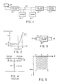
- a subscriber's telephone 10 is coupled to a telephone central office 11 via a conventional two-wire subscriber line 12.
- Modems 13 and 14 are also connected to the subscriber line 12 for transmitting data via the subscriber line between the locations of the telephone 10 and the central office 11, at a frequency, of for example 2lkHz, which is above the voice frequency band.
- these are coupled to the subscriber line 12 via low pass filters 15 and 16.
- Fig. 2 illustrates the attenuation of a low pass filter as a function of frequency.
- Each of the filters 15 and 16 is required to have a characteristic including a pass band up to a frequency fp in which the filter has a maximum attenuation ripple, or variation, Ap, and a stop band from a frequency fs in which the filter has a minimum attenuation As.
- fs 21kHz
- As 60dB
- fp 3200Hz
- Ap ⁇ O.ldB relative to the attenuation at 1000Hz.
- the low pass filter 15 is effectively driven by a voltage source 17 in series with an impedance Zl connected to an input port of the filter, and is loaded by an impedance Z2.
- the source 17 and impedance Z1 correspond to the telephone 10, while the impedance Z2 corresponds to the subscriber line 12, both typically having nominal impedances of 600 ohms.
- This program is used in known manner, initially being supplied with the desired characteristic values and resistive termination impedances Z1 and Z2 to determine a transfer function of the filter, and from this and the desired configuration of the filter to derive the form of a filter which satisfies the characteristic values and which is matched to the resistive termination impedances ZI and Z2.
- This typically results in the form of filter shown in Fig. 4, which is a 3rd order filter having series inductors 18, 19 and a shunt path including a capacitor 20 in series with an inductor 21.
- the elements 18 to 21 have values of 50.41mH, 50.41mH, 95.79nF, and 0.497mH respectively, as indicated in Fig. 4.
- Fig. 5 is a complex impedance graph, for a frequency of 3000Hz, illustrating the resistance R and reactance X of various points A to E.
- the point A of zero reactance and 600 ohm resistance, corresponds to the nominal termination impedances Zl and Z2 for which the filter of Fig. 4 is designed as described above.
- the subscriber line 12 is in practice not a purely resistive and accurately known impedance but a capacitive impedance which typically falls anywhere within the shaded area of Fig. 5, bounded by the points B, C, D, and E.
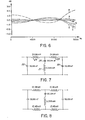
- Fig. 6 illustrates the attenuation of the filter of Fig. 4 in its passband up to 3000Hz, relative to its attenuation at 1000Hz, when the filter of Fig. 4 is terminated with impedances corresponding to each of the points A to E in Fig. 5.
- a filter such as that of Fig. 4, designed according to the prior art, can not be used with arbitrary subscriber lines 12 whose impedances fall anywhere within the shaded area of Fig. 5, if the design characteristics of the filter are to be satisfied.
- prior art filters must be individually designed for and/or matched to the subscriber lines with which they are to be used, in order to meet the required design characteristics.
- This individual design or matching is a great disadvantage because it is costly and time consuming and the filters are not readily interchangeable.
- much more complex and costly adaptive filters or buffered filters must be used.
- this disadvantage is very largely avoided or substantially eliminated by designing each of the low pass filters 15 and 16 in accordance with the desired characteristics already discussed, but with the additional constraint that the quantities
- Zl and Z2 are the nominal input and output, respectively, termination impedances of the filter as shown in Fig. 3 (which may in this case be complex impedances rather than purely resistive impedances as in the prior art)
- Zin is the input impedance of the filter at its input port
- Zout is the output impedance of the filter at its output port.
- conveniently their sum lZin-Z21 +
- the desired characteristic values fs, As, fp, and Ap and the nominal termination impedances Z1 and Z2 are used in the computer design program FILSYN to determine the transfer function of the filter, and from this and the desired configuration of the filter to determine a form of filter as in the prior art.
- the result is a 3rd order filter as already described.
- This determined form of filter is then optimized, preferably using the computer aided design program SCAMPER (see Telesis, Volume 7, Number 3, 1980, pages 2 to 9, published by Bell-Northern Research Ltd.), to provide the best possible filter response.
- the program SCAMPER is used with the additional constraint imposed in this program that the sum
- the SCAMPER program indicates that this can not be achieved with the number of variables provided by the determined form of the 3rd order filter. Accordingly, the FILSYN program is used again with the desired characteristic values and the nominal termination impedances with the additional requirement (not necessary in the prior art) that the filter be a higher order filter, e.g. a 5th order filter.
- a more restrictive pass band ripple Ap could be imposed upon the filter design using the FILSYN program, with a similar result.
- the resulting determined form of 5th order filter is then optimized using the SCAMPER program, again with the additional constraint imposed that the sum IZin-Z21 +
- the resulting 5th order filter is typically as shown in Fig. 7, comprising shunt capacitors 22, 23, series inductors 24, 25, and a shunt path including a capacitor 26 in series with an inductor 27.
- the elements 22 to 27 have values of 30.88nF, 30.88nF, 24.96mH, 24.96mH, 30.54nF, and 0.399mH respectively, as indicated in Fig. 7.
- the filter of Fig. 7 may be modified by providing the series inductances equally in the two wires of the filter, thereby balancing the filter.
- the series inductances are provided by four 12.48mH inductors.
- each series inductance 24, 25 can be divided equally between the two wires of the filter and constituted by two coupled coils to provide small size and good longitudinal balance.
- the two coils of each inductance 24, 25 are conveniently bifilar wound, the inductance of each individual coil, measured with the coil to which it is coupled open-circuit, then being 6.24mH.
- a solid line 28 illustrates the attenuation of the filter of Fig. 7, 8, or 9, relative to its attenuation at a frequency of 1000Hz, in the pass band up to 3000Hz.
- this attenuation is substantially the same throughout the passband regardless of the complex impedance, within the quadrant of the complex impedance graph of Fig. 5, with which the filter is terminated.
- the line 28 in Fig. 6 represents the filter attenuation in the passband for all of the points A to E in Fig. 5.
- the filter of Fig. 7, 8, or 9 can be used as each of the low pass filters 15 and 16 in Fig. 1 to provide the desired filter characteristics regardless of the nature of the particular subscriber line 12 which is used.
- this relatively simple filter can be used interchangeably, without requiring expensive buffering or adjustment, on arbitrary subscriber lines 12, the desired low pass filter characteristics always being satisfied.
- the shunt capacitor, for example 23 at the line 12 side of the low pass filter provides a low impedance across the line 12 for above voice-band signals. Consequently a problem arises in transmitting such signals between the modems 13 and 14 via the line 12 without excessive attenuation or loss of the signals due to the shunt capacitors of the filters. Furthermore, it is necessary to couple the modems 13 and 14 to the line 12 in such a manner that the design characteristics of the filters 15 and 16 are still complied with. This presents a significant problem in particular in maintaining the desired small attenuation ripple in the filter pass band.
- the signals transmitted from the modem 13 to the modem 14 may be FSK data signals at a center frequency of 36kHz and having actual frequencies of 35.5 and 36.5kHz
- the signals transmitted from the modem 14 to the modem 13 may be FSK data signals at a center frequency of 22kHz and having actual frequencies of 21.5 and 22.5kHz.
- These signal frequencies are assumed to be used in the following description, but other frequencies and types of signal transmission may be used.
- the line 12 is generally a balanced line, and it is therefore generally desired to couple the data signals between the line and the modems in a balanced manner.
- Fig. 10 shows a data coupling network with which the various desiderata above can be-met.
- Fig.,10 shows only the shunt capacitor 23 of the filter 15 or 16 at the line 12 side of the respective filter, the remainder of the filter being as illustrated in Fig. 7, 8, or 9.
- the data coupling network comprises a transformer 33 having a first winding 34 and two second windings 35 phased as shown by dots, inductors 36, 37, and 38, and capacitors 39 and 40.
- the second windings 35 of the transformer 33 are coupled in series with the filter capacitor 23, one on each side thereof, across the line 12.
- the first winding 34 of the transformer is connected between a wire 41 and circuit ground.
- the transformer With the wire 41 connected as described below, the transformer has a relatively small inductive reactance in the voice-band compared with the capacitive reactance of the capacitor 23, but the actual magnitude of this reactance is not critical because the low pass filter is designed to be insensitive to its terminations.
- the inductance of the transformer 33 measured across the first winding 34 with the capacitor 23 shorted and the second windings 35 open circuit, is relatively large (for example 8 to 10 times the inductance of the inductor 36) to avoid affecting the resonance described below of the inductor 36 with the capacitor 23.
- Transmit,data at the respective transmit frequency and present on a wire 42 is coupled to the wire 41 via the inductor 36.
- the inductance of the inductor 36 is selected so that it is series resonant with the filter capacitor 23, as reflected through the transformer 33, at the transmit frequency.
- the inductance of the inductor 37 which couples receive data from the wire 41 to a wire 43, is selected so that this inductor 37 is series resonant with the filter capacitor 23, as reflected through the transformer 33, at the respective receive frequency.
- the series inductors 36 and 37 therefore facilitate efficient coupling of transmit and receive data between the wires 42 and 43 and the line 12.
- the capacitor 40 is connected in parallel with the inductor 36 to form therewith a parallel resonant circuit which is resonant at the receive frequency.
- the inductor 38 and the capacitor 39 are also connected in parallel to form a parallel resonant circuit which is connected between the wire 41 and circuit ground.
- the values of the components 38 and 39 are selected so that this circuit is resonant at the respective transmit frequency, so that this resonant circuit presents an open circuit to, and does not attenuate, the transmit data on the line 41.
- this resonant circuit has a low impedance so that it is a virtual short circuit across the first winding 34 of the transformer 33. Consequently in the filter pass band the second windings 35 of the transformer are virtual short circuits, so that the capacitor 23 is effectively connected directly across the line 12 as in Figs. 7, 8, and 9 and the pass band characteristics of the low pass filter are not degraded.
- the parallel resonant circuit reduces the effects of impulse noise, for example due to dial pulsing, on circuits connected to the wires 42 and 43, because of its virtual short circuit at voice frequencies where most of the energy of such noise is concentrated.
- the parallel resonant circuit comprising the components 38 and 39 provides some attenuation of receive data at the receive frequency but this is readily compensated for by amplification of the receive data signals. This attenuation can be avoided by providing in place of the components 38 and 39 a more complicated circuit which is parallel resonant at both the receive and transmit frequencies, and has a low impedance in the voice-band.
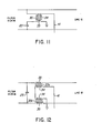
- Fig. 11 illustrates an alternative arrangement to that of Fig. 10, showing only the filter capacitor 23 and the transformer 33 and their connections, which can be used to couple data signals to and from an unbalanced line 12.
- the remainder of the coupling network in this case can be as illustrated in Fig. 10.
- the transformer 33 simply has in addition to the first winding 34 connected between the wire 41 and circuit ground, a single second winding 35 connected in series with the capacitor 23 across the line 12.
- This arrangement could also be used, if desired, for coupling .data signals to and from a balanced line 1.2, but the arrangement of Fig. 10 is preferred.
- Fig. 12 illustrates another alternative arrangement to that of Fig. 10, again showing only the filter capacitor 23 and the transformer 33 and their connections, which can be used to couple data signals to and from a balanced line 12.
- the remainder of the coupling network can be as illustrated in Fig. 10.
- the transformer 33 is divided into two parts 33a and 33b, each of which has a first winding 34 and a second winding 35.
- the first windings 34 are connected in series between the wire 41 and circuit ground.
- the second windings 35 are connected each in series with a respective wire of the line 12, whereby the filter capacitor 23 is again connected across the line 12 via these windings 35.
- the two parts 33a and 33b of the transformer could be combined into a single transformer 33 having a single first winding as shown in Fig. 10.
- the transformer arrangement shown in Fig. 10 is preferred over that of Fig. 12, because the latter arrangement contributes additional d.c. resistance to the subscriber loop including the line 12.
- the arrangement of Fig. 12 can be used if the additional d.c. resistance in the subscriber loop provided by the second windings 35.is acceptable.
- the components 38 and 39 may have magnitudes of 2.83mH and 18nF respectively for the transmit center frequency of 22kHz, and magnitudes of 4.6mH and 4.12nF respectively for the transmit center frequency of 36kHz.
- any means providing a relatively low impedance at frequencies in the pass band of the filter (e.g. the voice-band) to avoid degradation of the filter characteristics in the pass band, and providing a relatively high impedance to the signals to be coupled between the wire 41 and the line 12, may be coupled in parallel with the winding 34 in place of the specific parallel resonant circuit described.
- the parallel resonant circuit described constitutes a low pass filter connected in parallel with the winding 34, and any other suitable form of low pass filter could be used in its place.
- low pass filter for connection to a telephone subscriber line
- the principles of the invention can be applied to other than. low pass filters, e.g. to high pass and band pass filters, for connection to telephone subscriber lines, and can be applied to the design of low pass or other filters for use in other applications where variable or unknown termination impedances may be present.
- a high pass filter could be provided between each modem and the line 12, each high pass filter being designed in accordance with the invention to have the sum
- the form and order of the filter may vary from those described above, and in any event the particular impedances of the reactive components of the filter will be dependent upon the particular filter characteristics which are desired.
- the filter design described above uses the computer programs FILSYN and SCAMPER to determine the impedances of the reactive components of the filter, this being the preferred manner of effecting the filter design, the invention is not limited in this respect and other computer or manual design techniques may be used instead.
Landscapes
- Engineering & Computer Science (AREA)
- Computer Networks & Wireless Communication (AREA)
- Signal Processing (AREA)
- Power Engineering (AREA)
- Filters And Equalizers (AREA)
- Telephonic Communication Services (AREA)
- Cable Transmission Systems, Equalization Of Radio And Reduction Of Echo (AREA)
Applications Claiming Priority (4)
| Application Number | Priority Date | Filing Date | Title |
|---|---|---|---|
| CA000374737A CA1158789A (en) | 1981-04-06 | 1981-04-06 | Filters comprising reactive components, and a method of determining impedances thereof |
| CA374737 | 1981-04-06 | ||
| CA000392796A CA1165913A (en) | 1981-12-21 | 1981-12-21 | Apparatus for coupling signals to or from a two-wire line |
| CA392796 | 1981-12-21 |
Publications (3)
| Publication Number | Publication Date |
|---|---|
| EP0063414A2 true EP0063414A2 (de) | 1982-10-27 |
| EP0063414A3 EP0063414A3 (en) | 1984-08-01 |
| EP0063414B1 EP0063414B1 (de) | 1988-08-10 |
Family
ID=25669292
Family Applications (1)
| Application Number | Title | Priority Date | Filing Date |
|---|---|---|---|
| EP82301490A Expired EP0063414B1 (de) | 1981-04-06 | 1982-03-23 | Anordnung zum Ein-und Auskoppeln von Signalen in eine und aus einer Zweidrahtleitung |
Country Status (2)
| Country | Link |
|---|---|
| EP (1) | EP0063414B1 (de) |
| DE (1) | DE3278899D1 (de) |
Cited By (4)
| Publication number | Priority date | Publication date | Assignee | Title |
|---|---|---|---|---|
| GB2265777A (en) * | 1992-04-01 | 1993-10-06 | Plessey Telecomm | Suppressing unwanted signals in a transmission path |
| WO2000028660A1 (de) * | 1998-11-10 | 2000-05-18 | Vacuumschmelze Gmbh | Tiefpass für eine adsl-frequenzweiche |
| DE19959724C1 (de) * | 1999-12-10 | 2001-03-15 | Vacuumschmelze Gmbh | Tiefpaß für eine ADSL-Frequenzweiche |
| EP3817227A1 (de) * | 2019-11-04 | 2021-05-05 | Analog Devices International Unlimited Company | Leistungskombinierer bzw. leistungsteiler |
Family Cites Families (5)
| Publication number | Priority date | Publication date | Assignee | Title |
|---|---|---|---|---|
| FR959693A (de) * | 1950-03-31 | |||
| US1624682A (en) * | 1925-01-31 | 1927-04-12 | Western Electric Co | Electrical network |
| US3987375A (en) * | 1975-03-25 | 1976-10-19 | Stromberg-Carlson Corporation | Transmission bridge exhibiting reduced distortion |
| GB2042848B (en) * | 1978-12-30 | 1983-01-06 | Plessey Co Ltd | Line current feed and hybrid arrangement (sytem x) |
| US4378470A (en) * | 1981-03-25 | 1983-03-29 | Northern Telecom Limited | Interface circuits for connection to non-dedicated telephone lines |
-
1982
- 1982-03-23 DE DE8282301490T patent/DE3278899D1/de not_active Expired
- 1982-03-23 EP EP82301490A patent/EP0063414B1/de not_active Expired
Cited By (8)
| Publication number | Priority date | Publication date | Assignee | Title |
|---|---|---|---|---|
| GB2265777A (en) * | 1992-04-01 | 1993-10-06 | Plessey Telecomm | Suppressing unwanted signals in a transmission path |
| GB2265777B (en) * | 1992-04-01 | 1996-10-23 | Plessey Telecomm | Method and apparatus for supressing unwanted signals in a transmission path |
| WO2000028660A1 (de) * | 1998-11-10 | 2000-05-18 | Vacuumschmelze Gmbh | Tiefpass für eine adsl-frequenzweiche |
| DE19959724C1 (de) * | 1999-12-10 | 2001-03-15 | Vacuumschmelze Gmbh | Tiefpaß für eine ADSL-Frequenzweiche |
| WO2001043414A3 (de) * | 1999-12-10 | 2002-05-10 | Vacuumschmelze Gmbh & Co Kg | Tiefpass für eine adsl-frequenzweiche |
| EP3817227A1 (de) * | 2019-11-04 | 2021-05-05 | Analog Devices International Unlimited Company | Leistungskombinierer bzw. leistungsteiler |
| US11043931B2 (en) | 2019-11-04 | 2021-06-22 | Analog Devices International Unlimited Company | Power combiner/divider |
| US11843360B2 (en) | 2019-11-04 | 2023-12-12 | Analog Devices International Unlimited Company | Power combiner/divider |
Also Published As
| Publication number | Publication date |
|---|---|
| EP0063414B1 (de) | 1988-08-10 |
| EP0063414A3 (en) | 1984-08-01 |
| DE3278899D1 (en) | 1988-09-15 |
Similar Documents
| Publication | Publication Date | Title |
|---|---|---|
| US4443662A (en) | Filters comprising reactive components, and a method of determining impedances thereof | |
| US4456986A (en) | Apparatus for coupling signals to or from a two-wire line | |
| US4456985A (en) | Apparatus for coupling signals to or from a two-wire line | |
| US4800344A (en) | Balun | |
| US5705974A (en) | Power line communications system and coupling circuit for power line communications system | |
| US4717896A (en) | Balun | |
| US4764922A (en) | Data terminal interface circuit to a telephone transmission line | |
| US5528152A (en) | Method for measuring transmission parameters of balanced pair | |
| EP0677938A1 (de) | Signalkoppler | |
| US7386119B1 (en) | Filtered transmit cancellation in a full-duplex modem data access arrangement (DAA) | |
| US5719856A (en) | Transmitter/receiver interface apparatus and method for a bi-directional transmission path | |
| US4878244A (en) | Electronic hybrid circuit | |
| US4074087A (en) | Bidirectional voice frequency repeater | |
| EP0062442B1 (de) | Einrichtung für eine Zweidrahtleitung zum Einkoppeln oder Auskoppeln von Signalen | |
| US6804349B1 (en) | Hybrid transceiver circuit | |
| US6917682B2 (en) | Method and device for echo cancelling | |
| US4197431A (en) | Subscriber loop feed apparatus | |
| EP0063414A2 (de) | Anordnung zum Ein-und Auskoppeln von Signalen in eine und aus einer Zweidrahtleitung | |
| EP0691771A2 (de) | Kompensierter Hybridkoppler | |
| US7447305B2 (en) | Method and arrangement for filtering of signals | |
| CA1158789A (en) | Filters comprising reactive components, and a method of determining impedances thereof | |
| US4899365A (en) | Apparatus and method for adaptive amplitude equalization | |
| JPH04372213A (ja) | Lan用伝送インターフェース回路 | |
| CA1165914A (en) | Apparatus for coupling signals to or from a two-wire line | |
| CA1165913A (en) | Apparatus for coupling signals to or from a two-wire line |
Legal Events
| Date | Code | Title | Description |
|---|---|---|---|
| PUAI | Public reference made under article 153(3) epc to a published international application that has entered the european phase |
Free format text: ORIGINAL CODE: 0009012 |
|
| AK | Designated contracting states |
Designated state(s): DE FR GB IT NL SE |
|
| PUAL | Search report despatched |
Free format text: ORIGINAL CODE: 0009013 |
|
| AK | Designated contracting states |
Designated state(s): DE FR GB IT NL SE |
|
| 17P | Request for examination filed |
Effective date: 19840919 |
|
| GRAA | (expected) grant |
Free format text: ORIGINAL CODE: 0009210 |
|
| AK | Designated contracting states |
Kind code of ref document: B1 Designated state(s): DE FR GB IT NL SE |
|
| ITF | It: translation for a ep patent filed | ||
| REF | Corresponds to: |
Ref document number: 3278899 Country of ref document: DE Date of ref document: 19880915 |
|
| ET | Fr: translation filed | ||
| PLBI | Opposition filed |
Free format text: ORIGINAL CODE: 0009260 |
|
| 26 | Opposition filed |
Opponent name: SIEMENS AKTIENGESELLSCHAFT, BERLIN UND MUENCHEN Effective date: 19890510 |
|
| NLR1 | Nl: opposition has been filed with the epo |
Opponent name: SIEMENS AG |
|
| ITTA | It: last paid annual fee | ||
| PGFP | Annual fee paid to national office [announced via postgrant information from national office to epo] |
Ref country code: FR Payment date: 19920310 Year of fee payment: 11 |
|
| PGFP | Annual fee paid to national office [announced via postgrant information from national office to epo] |
Ref country code: GB Payment date: 19920316 Year of fee payment: 11 |
|
| PGFP | Annual fee paid to national office [announced via postgrant information from national office to epo] |
Ref country code: SE Payment date: 19920319 Year of fee payment: 11 |
|
| PGFP | Annual fee paid to national office [announced via postgrant information from national office to epo] |
Ref country code: NL Payment date: 19920331 Year of fee payment: 11 |
|
| PGFP | Annual fee paid to national office [announced via postgrant information from national office to epo] |
Ref country code: DE Payment date: 19920430 Year of fee payment: 11 |
|
| RDAG | Patent revoked |
Free format text: ORIGINAL CODE: 0009271 |
|
| STAA | Information on the status of an ep patent application or granted ep patent |
Free format text: STATUS: PATENT REVOKED |
|
| 27W | Patent revoked |
Effective date: 19920820 |
|
| GBPR | Gb: patent revoked under art. 102 of the ep convention designating the uk as contracting state |
Free format text: 920820 |
|
| NLR2 | Nl: decision of opposition | ||
| EUG | Se: european patent has lapsed |
Ref document number: 82301490.7 Effective date: 19930113 |