EP0063485A2 - Kompander für digitale Daten - Google Patents
Kompander für digitale Daten Download PDFInfo
- Publication number
- EP0063485A2 EP0063485A2 EP82301972A EP82301972A EP0063485A2 EP 0063485 A2 EP0063485 A2 EP 0063485A2 EP 82301972 A EP82301972 A EP 82301972A EP 82301972 A EP82301972 A EP 82301972A EP 0063485 A2 EP0063485 A2 EP 0063485A2
- Authority
- EP
- European Patent Office
- Prior art keywords
- signal
- digital input
- input signal
- digital
- set value
- Prior art date
- Legal status (The legal status is an assumption and is not a legal conclusion. Google has not performed a legal analysis and makes no representation as to the accuracy of the status listed.)
- Granted
Links
Images


Classifications
-
- H—ELECTRICITY
- H03—ELECTRONIC CIRCUITRY
- H03G—CONTROL OF AMPLIFICATION
- H03G7/00—Volume compression or expansion in amplifiers
- H03G7/007—Volume compression or expansion in amplifiers of digital or coded signals
-
- H—ELECTRICITY
- H03—ELECTRONIC CIRCUITRY
- H03M—CODING; DECODING; CODE CONVERSION IN GENERAL
- H03M7/00—Conversion of a code where information is represented by a given sequence or number of digits to a code where the same, similar or subset of information is represented by a different sequence or number of digits
- H03M7/30—Compression; Expansion; Suppression of unnecessary data, e.g. redundancy reduction
- H03M7/50—Conversion to or from non-linear codes, e.g. companding
Definitions
- the present invention relates to digital data companding (compression/expansion) and, more particularly, to digital data companding suitable for compressing the pulse code modulation (PCM) signal for recording or transfer and expanding the same for reproduction or retrieval.
- PCM pulse code modulation
- the analog signal is converted into the digital signal, such as in PCM system, for recording or transmission.
- the number of bits for recording or transmitting digital data is generally limited, and it is desirable to use the usable bits efficiently whereby to maintain a high S/N ratio.
- compression of data is carried out, i.e., a higher level signal is more attenuated relative to a lower level signal so that the maximum signal level is lowered.
- expansion of data is needed, i.e., a higher level signal is more amplified relative to a lower level signal.
- the circuit including both compressing and expanding abilities is called compander.
- the abscissa x represents the input, while the ordinate y represents the conversion output.
- the input x is classified into five ranges: x ⁇ -x2, -x2 ⁇ x. ⁇ -xl, -xl ⁇ x ⁇ +xl, +xl ⁇ x ⁇ +x2, and +x2 ⁇ x.
- the boundary between adjacent pair of ranges may belong to either one of the adjacent ranges. Since the characteristics for the ranges 0 ⁇ x and x ⁇ 0 are symmetric with respect to the origin, the case of 0 ⁇ x will solely be described in the following.
- the segment to which the data y belongs is identified by the range signal and the original signal x is reproduced in accordance with the transformation function designated to the identified segment.
- Figures 2A and 2B show examples of prior art circuits for compressing data as shown in Fig. 1.
- the sign bit in the highest bit position in digital data applied to the input terminal 51 is delivered directly through the line 58 to the output terminal 52.
- the remaining low order bits are fed to the shift register 56 and the range finder 54.
- the range finder 54 compares the input signal with the boundary values for the input (xl and x2 in Fig. 1) to determine which segment the input signal belongs to, and issues a range signal s to the shift register 56 and the range signal output terminal 53.
- Fig. 1 the sign bit in the highest bit position in digital data applied to the input terminal 51 is delivered directly through the line 58 to the output terminal 52.
- the remaining low order bits are fed to the shift register 56 and the range finder 54.
- the range finder 54 compares the input signal with the boundary values for the input (xl and x2 in Fig. 1) to determine which segment the input signal belongs to, and issues a range signal s to the shift register 56
- the range finder 54 includes a comparator 46 for comparing the input signal x with the first reference (boundary) value xl, a comparator 47 for comparing the input signal x with the second reference (boundary) value x2, and a decoder 48 for prcducing the range signal s based on the outputs from the comparators 46 and 47.
- the range finder 54 includes a comparator 49 and a control circuit 44 which provides the reference values xl and x2 sequentially to the comparator 49.
- the input data x loaded to the shift register 56 is shifted to the left by a certain number of bits (n-left shifts being equivalent to an operation of x/2 n ) according to the range signal s from the range finder 54 so that the low order bits are truncated for compression.
- n-left shifts being equivalent to an operation of x/2 n
- This method however, needs many range bits for carrying out a complex folded-encoding compression.
- selection of the boundaries of respective segments are very limited. These are disadvantageous in recording or transmitting as much data using as less bits.
- compressed data is offset so that it corresponds to the input in one-to-one correspondence, whereby to achieve efficient non-uniform folded-encoding companding without using range bits.
- the one-to-one correspondence does not hold to the low order bits which are truncated in the compressing process. Since no overlapping occurs in compressed data, the range signal is not needed and, moreover, the request for the limited selection of boundary values for respective ranges (segments) is eliminated. Accordingly, the polygonal line approximation which fits the desired companding characteristics can be configured arbitrarily.
- Fig. 3 illustrates a five-segment companding as in the case of Fig. 1.
- the abscissa x and ordinate-y of the graph represent the input and output, respectively. Since the companding characteristics for the input ranges 0 ⁇ x and x ⁇ 0 are symmetric with respect to the origin, the former case will solely be described in the following.
- the input x is classified by boundary values xl and x2 into three ranges each having a separate quantizing accuracy.
- the input is subjected to offset by +0, +a2 and +a3 as well as to scaling by xcl, xc2 and xc3, respectively.
- the scaling factors cl, c2 and c3 are chosen to satisfy cl > c2 >c3, so that the higher level input signal is more compressed.
- the offset factors a2 and a3 are chosen so that the y (and x) values of the segments S(l), S(2) and S(3) do not overlap with each other. In the embodiment shown in Fig.
- the offset factors are chosen such that the segments S(l) and S(2) would join at the boundary xl, and the segments S(2) and S(3) would join at the boundary x2.
- the input and output correspond in one-to-one relationship, without causing the overlap in the value of y, and thus the range signal is not necessary.
- boundaries for partitioning the whole input range can be set arbitrarily.
- multiplication (x c2) and addition (+ a2) can be carried out in arbitrary order.
- the order of multiplication (devision in the above equations) and addition (subtraction) is arbitrary as in the case of the compressing process.
- the factors c2 and c3 are smaller than one, and thus the result of multiplication (1/c3) x y can exceed the maximum value x M for the original signal x.
- this over-scaling can be anticipated without increasing the complexity of the circuit.
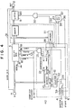
- FIG. 4 shows the case using one comparator
- Fig. 5 is the case using a plurality of comparators.
- a digital input termianl 1 is connected to and supplies digital input x to a shift register 6 and a comparator 9.
- An output terminal 2 is connected to a latch circuit 8 and also connected with a sign bit line 31, and sends out a digital output y.
- the mode input terminal 3 for the compression/expansion switching signal is connected directly and through an inverter 14 to the shift register 6 and also connected to memories (e.g. ROMs) 10 and 11, so that the switching signal designates the compressing operation or expanding operation.
- a clock input terminal 4 for the master clock signal is connected to a counter 12 and an AND gate 13, so that the clock signal provides the timing for input range discrimination.
- An input terminal 5 for the start signal is connected to the counter 12, shift register 6 and D-type flip-flop 33, so that the signal initializes or resets the whole circuit upon receipt of a new input.
- the shift register 6 has a grounded serial input terminal 15 for entering 0's bits and for truncating the low order bits, right and left shift signal input terminals 17 and 16 for selecting the right shift or left shift operation, clock signal input terminal 18 for carrying out the bitshift operation, and load signal input terminal 19 for fetching new data.
- An adder 7 is connected to the output of the shift register 6 and the output of the memory 11, so that an offset value from the memory 11 is added to a compressed data from the shift register 6. The resultant data is fed to the latch circuit 8.
- a signal which has been converted into digital data by an A/D converter (not shown in the figure) is applied to the input terminal 1.
- the sign bit in the highest bit position of the input data is conducted directly through the line 31 to the output terminal 2.
- the remaining low order 13 bits are fed to the shift register 6 and the magnitude comparator 9.
- the start signal is applied to the start signal input terminal 5, the circuit starts operating by loading the input'data to the shift register 6 and clearing the counter 12 and flip-flop 33.
- the boundary values and offset values are read out from the memories 10 and 11 in response to the output of the counter 12 which is the input range number obtained by counting the master clock signal entered through the master clock terminal 4.
- the first boundary value xl e.g. 1023
- the comparator 9 If the input data x at the comparator input terminal 21 is larger than the reference signal xl, the output 23 of the comparator 9 provides a high level. This high level signal is fed via an AND gate 13 to the clock input termianl 18 of the shift register 6, whose contents are then shifted to the left by one bit.
- the data x is discriminated to belong to the first input range (0 ⁇ x ⁇ xl), causing another output 24 of the comparator 9 to go high level.
- This signal triggers the latch circuit 8 through an AND gate 32, so that the input data added by the offset value (zero offset for the first input range) by the adder 7 is latched and delivered to the output terminal 2.
- the data transformation as shown by the segment S(l) of Fig. 3 is carried out.
- the D-type flip-flop 33 provides a low level at its output 37 so that the latch circuit 8 does not latch the subsequent incoming signal.
- the boundary value x2 e.g. 6143
- the compression operation is then completed. It will be understood that the output data y has 13 bits including the highest order sign bit and 12 lower order bits.
- compressed data may be contiguous at the boundary of segments. Alternatively, they may have a gap at the boundary.
- the offset value varies depending on the boundary values of segmented lines.
- boundary values yl and y2
- offset values are different from those of the compressing process.
- the compression/expansion switching signal which may be produced, for example, by operating the recording/reproduction switch such that the high level signal is applied to the left-shift terminal 16 of the shift register 6 for recording (compression), while the low level signal is inverted by the inverter 14 and applied to the right-shift terminal 17 for reproduction (expansion).
- the offset value is subtracted in the expanding preocess, and this operation can be carried out in a similar way as in the compressing process by storing the negative offset values in the ROM 11. Similar to the compression, the order of substruction (addition) and miltiplication (division) may be changed.
- a clock control circuit 39 (shown by the dashed block in Fig. 4) may be provided in the clock signal path instead of using the D-type flip-flop 33, AND gate 32 and latch circuit 8, so that the output of the adder 7 is fixed by halting the clock signal.
- Figure 5 shows another embodiment of the companding circuit, wherein a plurality of comparators are used for comparing boundary values separately. Also in this case, the latch circuit and the accompanied components can be eliminated.
- like numbers signify like circuit components.
- the first comparator 46 compares input signal x with the first reference value xl, while the second comparator 47 compares the input signal x with the second reference value x2.
- the outputs of both comparators are converted into a range signal by the decoder 48, then delivered to the shift register 6 and memory 11.
- the offset value supplied from the memory 11 is added to the compressed (expanded) signal which has been shifted in accordance with the identified input range, and the resultant compression output y is delivered to the output terminal 2.
- the decoder 48 can be eliminated if the shift register 6 and memory 11 are driven directly by the output of the comparators 46 and 47.
- the present invention eliminates the need of range bits and allows arbitrary setting of boundaries in non-uniform folded companding, whereby data can be compressed efficiently. Moreover, the compressing and expanding operations can be carried out by the same circuit.
Landscapes
- Physics & Mathematics (AREA)
- Nonlinear Science (AREA)
- Engineering & Computer Science (AREA)
- Theoretical Computer Science (AREA)
- Compression, Expansion, Code Conversion, And Decoders (AREA)
Applications Claiming Priority (4)
| Application Number | Priority Date | Filing Date | Title |
|---|---|---|---|
| JP58532/81 | 1981-04-20 | ||
| JP5853281A JPS57173239A (en) | 1981-04-20 | 1981-04-20 | Polygonal line compressing and expanding circuit |
| JP37986/82 | 1982-03-12 | ||
| JP3798682A JPS58156239A (ja) | 1982-03-12 | 1982-03-12 | 折線圧縮伸張回路 |
Publications (3)
| Publication Number | Publication Date |
|---|---|
| EP0063485A2 true EP0063485A2 (de) | 1982-10-27 |
| EP0063485A3 EP0063485A3 (en) | 1984-06-06 |
| EP0063485B1 EP0063485B1 (de) | 1988-10-05 |
Family
ID=26377167
Family Applications (1)
| Application Number | Title | Priority Date | Filing Date |
|---|---|---|---|
| EP82301972A Expired EP0063485B1 (de) | 1981-04-20 | 1982-04-16 | Kompander für digitale Daten |
Country Status (3)
| Country | Link |
|---|---|
| US (1) | US4682152A (de) |
| EP (1) | EP0063485B1 (de) |
| DE (1) | DE3279093D1 (de) |
Cited By (2)
| Publication number | Priority date | Publication date | Assignee | Title |
|---|---|---|---|---|
| EP0118144A1 (de) * | 1983-02-08 | 1984-09-12 | Koninklijke Philips Electronics N.V. | Digitaler Dynamikbereichumsetzer |
| EP0394976A3 (en) * | 1989-04-27 | 1990-12-05 | Matsushita Electric Industrial Co., Ltd. | Data companding method and data compressor/expander |
Families Citing this family (7)
| Publication number | Priority date | Publication date | Assignee | Title |
|---|---|---|---|---|
| JP2702126B2 (ja) * | 1987-08-20 | 1998-01-21 | パイオニア株式会社 | データ出力回路 |
| JP2775857B2 (ja) * | 1989-06-20 | 1998-07-16 | ソニー株式会社 | デジタル信号の帯域圧縮回路 |
| US5629884A (en) * | 1995-07-28 | 1997-05-13 | Motorola, Inc. | Log converter utilizing offset and method of use thereof |
| KR100378162B1 (ko) * | 2000-01-11 | 2003-03-29 | 삼성전자주식회사 | 룩업 테이블을 이용한 연산결과 검출장치 및 방법 |
| US6883012B1 (en) | 2001-03-19 | 2005-04-19 | Cisco Systems Wireless Networking (Australia) Pty Limited | Linear-to-log converter for power estimation in a wireless data network receiver |
| US7671778B2 (en) * | 2003-06-18 | 2010-03-02 | General Instrument Corporation | Digital signal processing scheme for high performance HFC digital return path system with bandwidth conservation |
| DE102004041418A1 (de) * | 2004-08-26 | 2006-03-09 | Micronas Gmbh | Verfahren zur Codierung eines ersten und zweiten Datenwortes und Verfahren zur Decodierung eines codierten Datenwortes |
Family Cites Families (10)
| Publication number | Priority date | Publication date | Assignee | Title |
|---|---|---|---|---|
| US3610901A (en) * | 1969-09-09 | 1971-10-05 | Emerson Electric Co | Digital modified discrete fourier transform doppler radar processor |
| US3694639A (en) * | 1970-04-07 | 1972-09-26 | Pierre A Deschenes | Pulse code modulation digital compandor |
| US3863248A (en) * | 1973-01-02 | 1975-01-28 | Univ Sherbrooke | Digital compressor-expander |
| JPS5534613B2 (de) * | 1973-10-08 | 1980-09-08 | ||
| US4078250A (en) * | 1974-08-21 | 1978-03-07 | The Singer Company | Log-antilog conversion for a digital radar system |
| DE2505388C2 (de) * | 1975-02-08 | 1983-06-23 | Philips Patentverwaltung Gmbh, 2000 Hamburg | Anordnung zur logarithmischen Umwandlung eines Meßwertes |
| US4058676A (en) * | 1975-07-07 | 1977-11-15 | International Communication Sciences | Speech analysis and synthesis system |
| US4267579A (en) * | 1979-07-13 | 1981-05-12 | Norlin Industries, Inc. | Digital waveform generator having constant signal to noise ratio |
| US4342245A (en) * | 1979-10-26 | 1982-08-03 | Norlin Industries, Inc. | Complex waveform generator for musical instrument |
| US4326260A (en) * | 1980-07-07 | 1982-04-20 | Norlin Industries, Inc. | Linear piecewise waveform generator for an electronic musical instrument |
-
1982
- 1982-04-15 US US06/368,868 patent/US4682152A/en not_active Expired - Fee Related
- 1982-04-16 DE DE8282301972T patent/DE3279093D1/de not_active Expired
- 1982-04-16 EP EP82301972A patent/EP0063485B1/de not_active Expired
Cited By (3)
| Publication number | Priority date | Publication date | Assignee | Title |
|---|---|---|---|---|
| EP0118144A1 (de) * | 1983-02-08 | 1984-09-12 | Koninklijke Philips Electronics N.V. | Digitaler Dynamikbereichumsetzer |
| EP0394976A3 (en) * | 1989-04-27 | 1990-12-05 | Matsushita Electric Industrial Co., Ltd. | Data companding method and data compressor/expander |
| US5047768A (en) * | 1989-04-27 | 1991-09-10 | Matsushita Electric Industrial Co., Ltd. | Data companding method and data compressor/expander |
Also Published As
| Publication number | Publication date |
|---|---|
| EP0063485A3 (en) | 1984-06-06 |
| DE3279093D1 (de) | 1988-11-10 |
| US4682152A (en) | 1987-07-21 |
| EP0063485B1 (de) | 1988-10-05 |
Similar Documents
| Publication | Publication Date | Title |
|---|---|---|
| US5254991A (en) | Method and apparatus for decoding Huffman codes | |
| EP0178813B1 (de) | Verfahren und Vorrichtung zur numerischen Datenkodierung | |
| US4044347A (en) | Variable-length to fixed-length conversion of minimum-redundancy codes | |
| US4559563A (en) | Adaptive prediction for binary encoded documents containing a mixture of text, line drawings and halftones | |
| EP0177950A2 (de) | Verfahren zur Kodierung eines digitalen Informationssignals | |
| EP0469841A1 (de) | Datenrundungsvorrichtung | |
| US5028926A (en) | Successive type analog-to-digital converter with a variable reference voltage for the digital to analog converter | |
| US5008668A (en) | Method and apparatus for encoding and decoding data in residue number system | |
| US5353024A (en) | Method for data compression having an improved encoding algorithm which utilizes a token stacking technique | |
| GB2113945A (en) | Picture digital processing | |
| US5107519A (en) | Coding device and a decoding device | |
| US5115241A (en) | Predictive coding device with increased resolution | |
| JP3410629B2 (ja) | 可変長符号化回路及び可変長符号化方法 | |
| AU695626B2 (en) | Video image colour encoding | |
| EP0063485A2 (de) | Kompander für digitale Daten | |
| US3863248A (en) | Digital compressor-expander | |
| US5270716A (en) | Digital-to-analog converter with high linearity | |
| JPS60235587A (ja) | ビデオ信号フエーデイング回路 | |
| US4447829A (en) | Facsimile transmission arrangement | |
| JPH05284035A (ja) | 情報変換方法 | |
| US3984833A (en) | Apparatus for encoding extended run-length codes | |
| US5303372A (en) | Pipelined image data compression system | |
| US4037226A (en) | Pulse code modulation compressor | |
| US4736387A (en) | Quantizing apparatus | |
| US5724277A (en) | Background noise generating apparatus |
Legal Events
| Date | Code | Title | Description |
|---|---|---|---|
| PUAI | Public reference made under article 153(3) epc to a published international application that has entered the european phase |
Free format text: ORIGINAL CODE: 0009012 |
|
| AK | Designated contracting states |
Designated state(s): DE FR GB |
|
| PUAL | Search report despatched |
Free format text: ORIGINAL CODE: 0009013 |
|
| AK | Designated contracting states |
Designated state(s): DE FR GB |
|
| 17P | Request for examination filed |
Effective date: 19841109 |
|
| GRAA | (expected) grant |
Free format text: ORIGINAL CODE: 0009210 |
|
| AK | Designated contracting states |
Kind code of ref document: B1 Designated state(s): DE FR GB |
|
| REF | Corresponds to: |
Ref document number: 3279093 Country of ref document: DE Date of ref document: 19881110 |
|
| ET | Fr: translation filed | ||
| PLBE | No opposition filed within time limit |
Free format text: ORIGINAL CODE: 0009261 |
|
| STAA | Information on the status of an ep patent application or granted ep patent |
Free format text: STATUS: NO OPPOSITION FILED WITHIN TIME LIMIT |
|
| 26N | No opposition filed | ||
| PGFP | Annual fee paid to national office [announced via postgrant information from national office to epo] |
Ref country code: FR Payment date: 19930219 Year of fee payment: 12 |
|
| PGFP | Annual fee paid to national office [announced via postgrant information from national office to epo] |
Ref country code: GB Payment date: 19930405 Year of fee payment: 12 |
|
| PGFP | Annual fee paid to national office [announced via postgrant information from national office to epo] |
Ref country code: DE Payment date: 19930629 Year of fee payment: 12 |
|
| PG25 | Lapsed in a contracting state [announced via postgrant information from national office to epo] |
Ref country code: GB Effective date: 19940416 |
|
| GBPC | Gb: european patent ceased through non-payment of renewal fee |
Effective date: 19940416 |
|
| PG25 | Lapsed in a contracting state [announced via postgrant information from national office to epo] |
Ref country code: FR Effective date: 19941229 |
|
| PG25 | Lapsed in a contracting state [announced via postgrant information from national office to epo] |
Ref country code: DE Effective date: 19950103 |
|
| REG | Reference to a national code |
Ref country code: FR Ref legal event code: ST |